CC1190
www.ti.com
SWRS089 A – NOVEMBER 2009 – REVISED FEBRUARY 2010
850 – 950 MHz RF Front End
Check for Samples: CC1190
FEATURES
APPLICATIONS
•
•
•
•
•
•
•
•
1
•
•
•
•
•
•
•
•
•
•
Seamless Interface to Sub-1 GHz Low Power
RF Devices from Texas Instruments
Up to 27 dBm (0.5 W) Output Power
6 dB Typical Sensitivity Improvement with
CC11xx and CC430
Few External Components
– Integrated PA
– Integrated LNA
– Integrated Switches
– Integrated Matching Network
– Integrated Inductors
Digital Control of LNA and PA Gain by HGM
Pin
50-nA in Power Down (LNA_EN = PA_EN = 0)
High Transmit Power Efficiency
– PAE = 50% at 26 dBm Output Power
Low Receive Current Consumption
– 3 mA for High Gain Mode
– 26 µA for Low Gain Mode
2.9 dB LNA Noise Figure, Including Switch and
External Antenna Match
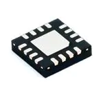
RoHS Compliant 4-mm × 4-mm QFN-16
Package
2 V to 3.7 V Operation
850 - 950 MHz ISM Bands Wireless Systems
Wireless Sensor Networks
Wireless Industrial Systems
IEEE 802.15.4 Systems
Wireless Consumer Systems
Wireless Metering (AMR/AMI) Systems
Smart Grid Wireless Networks
DESCRIPTION
CC1190 is a cost-effective and high-performance RF
Front End for low-power and low-voltage wireless
applications at 850 - 950 MHz.
CC1190 is a range extender for the sub-1 GHz
low-power RF transceivers, transmitters, and
System-on-Chip devices from Texas Instruments.
CC1190 integrates a power amplifier (PA), a
low-noise amplifier (LNA), switches, and RF matching
for the design of a high-performance wireless
systems.
CC1190 increases the link budget by providing a
power amplifier for increased output power, and an
LNA with low noise figure for improved receiver
sensitivity.
CC1190 provides an efficient and easy-to-use range
extender in a compact 4-mm × 4-mm QFN-16
package.
CC1190 BLOCK DIAGRAM
VDD_LNA
VDD_PA1 VDD_PA2
PA_OUT
PA
PA_IN
PREAMP
EN
EN
TR_SW
LNA_OUT
LNA
EN
LNA_IN
LOGIC
PA_EN
LNA_EN
BIAS
BIAS
HGM
1
Please be aware that an important notice concerning availability, standard warranty, and use in critical applications of Texas
Instruments semiconductor products and disclaimers thereto appears at the end of this data sheet.
PRODUCTION DATA information is current as of publication date.
Products conform to specifications per the terms of the Texas
Instruments standard warranty. Production processing does not
necessarily include testing of all parameters.
Copyright © 2009–2010, Texas Instruments Incorporated
�CC1190
SWRS089 A – NOVEMBER 2009 – REVISED FEBRUARY 2010
www.ti.com
These devices have limited built-in ESD protection. The leads should be shorted together or the device placed in conductive foam
during storage or handling to prevent electrostatic damage to the MOS gates.
ORDERING INFORMATION
DEVICE
TEMPERATURE
PACKAGE (1)
-40°C to 85°C
QFN (RVG) 16
CC1190RGVR
CC1190RGVT
(1)
TRANSPORTION MEDIA
Tape and Reel, 2500
Tape and Reel, 250
For the most current package and ordering information, see the Package Option Addendum at the end of this document, or see the TI
website at www.ti.com.
ABSOLUTE MAXIMUM RATINGS
Under no circumstances must the absolute maximum ratings be violated. Stress exceeding one or more of the limiting values
may cause permanent damage to the device.
Supply voltage, VDD
All supply pins must have the same voltage
Voltage on any digital pin
VALUE
UNIT
–0.3 to 3.8
V
–0.3 to VDD + 0.3, max 3.8
V
10
dBm
Input RF level
Storage temperature range
ESD
–50 to 150
°C
Human-body model, non RF pins
2000
V
Human-body model, RF pins: PA_IN, PA_OUT, TR_SW,
LNA_IN, LNA_OUT
1500
V
Charged device model
1000
V
RECOMMENDED OPERATING CONDITIONS
Ambient temperature range
MIN
MAX
–40
85
°C
2
3.7
V
850
950
MHz
Operating supply voltage
Operating frequency range
UNIT
ELECTRICAL CHARACTERISTICS
TC = 25°C, VDD = 3 V, fRF = 915 MHz (unless otherwise noted). Measured on CC1190EM reference design including external
matching components optimized for 915 MHz operation.
PARAMETER
Receive current
TEST CONDITIONS
MIN
2
MAX
UNIT
3
mA
PIN = -40 dBm, HGM = 0
26
µA
PIN = 5 dBm, POUT = 26.5 dBm, HGM = 1
Transmit current
TYP
PIN = -40 dBm, HGM = 1
302
No input signal, HGM = 1
56
No input signal, HGM = 0
29
Power down current
LNA_EN = PA_EN = 0
High input level (control pins)
HGM, LNA_EN, PA_EN
Low input level (control pins)
HGM, LNA_EN, PA_EN
50
1.3
mA
200
nA
VDD
V
0.3
V
Power down → Receive mode, switching
time
300
ns
Power down → Transmit mode, switching
time
600
ns
Submit Documentation Feedback
Copyright © 2009–2010, Texas Instruments Incorporated
Product Folder Link(s) :CC1190
�CC1190
www.ti.com
SWRS089 A – NOVEMBER 2009 – REVISED FEBRUARY 2010
ELECTRICAL CHARACTERISTICS (continued)
TC = 25°C, VDD = 3 V, fRF = 915 MHz (unless otherwise noted). Measured on CC1190EM reference design including external
matching components optimized for 915 MHz operation.
PARAMETER
TEST CONDITIONS
MIN
TYP
MAX
UNIT
RF Receive
Gain
PIN = -40 dBm, HGM = 1
11.6
PIN = -40 dBm, HGM = 0
-6
Gain variation over frequency
850–950 MHz, PIN = -40 dBm, HGM = 1
Gain variation over power supply
2 – 3.7 V, PIN = -40 dBm, HGM = 1
Noise figure
1.2
dB
1
dB
HGM = 1, including internal switch and external
antenna match
2.9
dB
HGM = 0, including internal switch and external
antenna match
6.2
dBm
HGM = 1
-12.3
HGM = 0
11.2
Input IP3, High Gain Mode
HGM = 1
-5
Input reflection coefficient, S11, High
Gain Mode
HGM = 1, measured at antenna port, depends
on external antenna and LNA match
Input 1 dB compression
dB
-11.5
dBm
dBm
dB
RF Transmit
Gain
Maximum Output Power
Output power, POUT
PIN = -20 dBm, HGM = 1
27.9
PIN = -20 dBm, HGM = 0
24.6
PIN = 5 dBm, HGM = 1, VDD = 3.7 V
27.7
PIN = 5 dBm, HGM = 1
26.5
PIN = 0 dBm, HGM = 1
25.5
PIN = -6 dBm, HGM = 1
Power Added Efficiency, PAE
Output 1 dB compression
Output power variation over frequency
PIN = 5 dBm, HGM = 1
24
23.7
Output power variation over temperature
-40°C – 85°C, PIN = 5 dBm, HGM = 1
2nd harmonic power
HGM = 1, PIN = 5 dBm
See application note AN001 (SWRA090) for
regulatory requirements.
3rd harmonic power
Input reflection coefficient, S11
HGM = 1, measured at SMA connector on
PA_IN/LNA_OUT (TX active)
Product Folder Link(s) :CC1190
dBm
1.7
dB
4.5
dB
1
dB
2.5
-37
-10
Submit Documentation Feedback
Copyright © 2009–2010, Texas Instruments Incorporated
dBm
48%
HGM = 0
Output power variation over power supply 2 V – 3.7 V, PIN = 5 dBm, HGM = 1
dBm
22
HGM = 1
850 – 950 MHz, PIN = 5 dBm, HGM = 1
dB
dBm
dB
3
�CC1190
SWRS089 A – NOVEMBER 2009 – REVISED FEBRUARY 2010
www.ti.com
DEVICE INFORMATION
GND
1
PA_OUT
2
VDD_PA1
VDD_PA2
BIAS
VDD_LNA
QFN-16 PACKAGE
TOP VIEW
16
15
14
13
12
GND
11
PA_IN
10
LNA_OUT
4x4 QFN-16
9
5
6
7
8
PA_EN
4
LNA_EN
TR_SW
HGM
3
LNA_IN
GND
GND
NOTE
The exposed die attach pad must be connected to a solid ground plane as this is the
primary ground connection for the chip. Inductance in vias to the pad should be
minimized. Following the CC1190EM reference layout is recommended. Changes will alter
the performance. Also see the PCB land pattern information in this data sheet.
PIN FUNCTIONS
PIN
4
I/O
DESCRIPTION
NO.
NAME
-
GND
Ground
The exposed die attach pad must be connected to a solid ground plane. See CC1190EM
(SWRR064) reference design for recommended layout.
1
GND
Ground
Secondary ground connection. Should be shorted to the die attach pad on the top PCB layer.
2
PA_OUT
RF
3
GND
Ground
4
TR_SW
RF
RXTX switch pin.
5
LAN_IN
RF
Input of LNA.
6
HGM
Digital Input
Digital control pin.
HGM = 1 → Device in High Gain Mode.
HGM = 0 → Device in Low Gain Mode.
7
LNA_EN
Digital Input
Digital control pin. See Table 2 and Table 3 for details.
8
PA_EN
Digital Input
Digital control pin. See Table 2 and Table 3 for details.
9
GND
Ground
10
LNA_OUT
RF
Output of LNA.
11
PA_IN
RF
Input of PA.
12
GND
Ground
Secondary ground connection. Should be shorted to the die attach pad on the top PCB layer.
13
VDD_LNA
Power
2 – 3.7 V Supply Voltage.
14
BIAS
Analog
Biasing input. Resistor between this node and ground sets bias current.
15
VDD_PA2
Power
2 – 3.7 V Supply Voltage.
16
VDD_PA1
Power
2 – 3.7 V Supply Voltage.
Output of PA.
Secondary ground connection. Should be shorted to the die attach pad on the top PCB layer.
Secondary ground connection. Should be shorted to the die attach pad on the top PCB layer.
Submit Documentation Feedback
Copyright © 2009–2010, Texas Instruments Incorporated
Product Folder Link(s) :CC1190
�CC1190
www.ti.com
SWRS089 A – NOVEMBER 2009 – REVISED FEBRUARY 2010
CC1190EM Evaluation Module
L23
C21
PA_OUT
C28
C25
C24
VDD_LNA
L24
VDD_PA1
L21
SMA
VDD_PA2
VDD
VDD
C111
SMA
PA_IN
LNA_OUT
L22
C101
C22
CC1190
TR_SW
PA_EN
C51
PA_EN
LNA_EN
LNA_IN
LNA_EN
HGM
BIAS
HGM
R141
Figure 1. CC1190EM Evaluation Module
Table 1. List of Materials Optimized for 915 MHz Operation
(See the CC1190EM Reference Design, SWRR064)
DEVICE
FUNCTION
VALUE
L21
PA load inductor
10 nH, LQW18AN10NG10 from Murata
L22
RXTX switch and LNA match
7.5 nH, LQW15AN7N5G00 from Murata
L23
Part of antenna match
2.2 nH, LQW15AN2N2C10D from Murata
L24
Part of antenna match
3.9 nH, LQW15AN3N9C00 from Murata
C21
DC block
47 pF, GRM1555C1H470JZ01D from Murata
C22
RXTX switch and LNA match
12 pF, GRM1555C1H120JZ01D from Murata
C24
Part of antenna match
3.3 pF: GRM1555C1H3R3CZ01D from Murata
C25
Part of antenna match
8.2 pF: GRM1555C1H8R2CZ01D from Murata
C28
Part of antenna match
0.5 pF, GRM1555C1HR50CZ01D from Murata
C51
Part of LNA match
12 pF, GRM1555C1H120JZ01D from Murata
C101
DC block
47 pF: GRM1555C1H470JZ01D from Murata
C111
DC block
47 pF: GRM1555C1H470JZ01D from Murata
R141
Bias resistor
3.3 kΩ, RK73H1ETTP3301F from Koa
Submit Documentation Feedback
Copyright © 2009–2010, Texas Instruments Incorporated
Product Folder Link(s) :CC1190
5
�CC1190
SWRS089 A – NOVEMBER 2009 – REVISED FEBRUARY 2010
www.ti.com
TYPICAL CHARACTERISTICS
TC = 25°C, VDD = 3 V, fRF = 915 MHz (unless otherwise noted). Measured on CC1190EM reference design including external
matching components optimized for 915 MHz operation.
11.7
GAIN
-5
-5.2
11.5
11.3
2.95
11.1
2.90
10.9
NF
2.85
HGM GAIN
-5.4
12.0
HGM Gain - dB
3.00
LNA Gain in HGM - dB
Noise Figure in HGM - dB
3.05
12.5
-5.6
-5.8
11.5
LGM GAIN
-6
-6.2
11.0
10.7
2.80
850 860
870
880 890
900
910
920
-6.4
10.5
940 950
930
LGM Gain - dB
3.10
10.5
-40 -30 -20 -10
0
10 20
-6.6
30 40 50 60 70 80 90
o
Frequency - MHz
Temperature - C
Figure 2. LNA Gain and Noise Figure vs Operating Frequency
Figure 3. LNA Gain vs Temperature
SPACER
-5.8
12.0
-5.85
11.9
HGM GAIN
LGM GAIN
11.6
-6
11.5
-6.05
11.4
-6.1
11.3
-6.15
11.2
S (1,1)
HGM Gain - dB
-5.95
11.7
LGM Gain - dB
-5.9
11.8
-6.2
2
2.2
2.4
2.6
2.8
3
3.2
3.4
3.6
Supply Voltage - V
Frequency (850 MHz to 950 MHz)
Figure 5. Input Impedance of LNA Measured from Antenna Port
on CC1190EM (RX Active)
60
400
60
50
350
55
40
300
50
360
340
250
200
20
POUT
10
150
I_VDD
PAE - %, POUT - dBm
PAE
30
Current - mA
PAE - %, POUT - dBm
I_VDD
300
40
280
35
260
100
-10
50
25
0
20
850 860
-35
-30
-25
-20
-15
-10
-5
0
5
30
240
POUT
220
870 880 890
900 910 920 930
940
200
950
Frequency - MHz
Pin - dBm
Figure 6. PA Output Power, PAE and Current Consumption
vs Input Power
6
320
45
0
-20
-40
PAE
Current - mA
Figure 4. LNA Gain vs Supply Voltage
Figure 7. PA Output Power, PAE and Current Consumption
vs Operating Frequency at 5 dBm Input Power
Submit Documentation Feedback
Copyright © 2009–2010, Texas Instruments Incorporated
Product Folder Link(s) :CC1190
�CC1190
www.ti.com
SWRS089 A – NOVEMBER 2009 – REVISED FEBRUARY 2010
TYPICAL CHARACTERISTICS (continued)
TC = 25°C, VDD = 3 V, fRF = 915 MHz (unless otherwise noted). Measured on CC1190EM reference design including external
matching components optimized for 915 MHz operation.
50
340
50
320
300
45
I_VDD
40
280
260
35
30
240
POUT
25
20
-40 -30 -20 -10
0
10 20
30
40
50 60
PAE
325
300
45
275
40
I_VDD
35
250
30
220
25
200
20
70 80
350
Current - mA
PAE
55
Current - mA
PAE - %, POUT - dBm
55
360
PAE - %, POUT - dBm
60
225
POUT
200
175
2
2.2
o
2.4
2.6
2.8
3
3.2
3.4
3.6
Supply Voltage - V
Temperature - C
Figure 9. PA Output Power, PAE and Current Consumption
vs Supply Voltage at 5 dBm Input Power
S (1,1)
Figure 8. PA Output Power, PAE and Current Consumption
vs Temperature at 5 dBm Input Power
Frequency (850 MHz to 950 MHz)
Figure 10. Input Impedance Measured at SMA connector on PA_IN/LNA_OUT on CC1190EM (TX Active)
Submit Documentation Feedback
Copyright © 2009–2010, Texas Instruments Incorporated
Product Folder Link(s) :CC1190
7
�CC1190
SWRS089 A – NOVEMBER 2009 – REVISED FEBRUARY 2010
www.ti.com
INTERFACE AND CONTROL
Controlling the Output Power from CC1190
The output power of CC1190 is controlled by controlling the input power. The CC1190 PA is designed to work in
compression (class AB), and the best efficiency is reached when a strong input signal is applied. The output
power can be reduced by setting the pin HGM low. If a reduced maximum output power is wanted, the
impedance seen by the PA should be increased, thus increasing the PA efficiency by changing the output
matching network.
Input Levels on Control Pins
The three digital control pins (PA_EN, LNA_EN, HGM) have built-in level-shifting functionality, meaning that if
CC1190 is operating from a 3.6 V supply voltage, the control pins will still sense 1.6 - 1.8 V signals as logical '1'.
An example of the above is that PA_EN is connected directly to the PA_EN pin on CC110x, but the global supply
voltage is 3.6 V. The PA_EN pin on CC110x will switch between 0 V (RX) and 1.8 V (TX), and this is still a high
enough voltage to control the operating mode of CC1190.
However, the input voltages should not have logical '1' level that is higher than the supply.
Connecting CC1190 to a CC102X Device
Table 2. Control Logic for Connecting CC1190 to a CC102X Device
PA_EN
LNA_EN
HGM
Mode Of Operation
0
0
don't care
Power Down
0
1
0
RX Low Gain Mode
0
1
1
RX High Gain Mode
1
0
0
TX Low Gain Mode
1
0
1
TX High Gain Mode
VDD_LNA
VDD_PA1
VDD_PA2
VDD
PA_IN
LNA_OUT
RF_OUT
SAW
RF__IN
PA_OUT
CC102X
CC1190
TR_SW
PA_EN
BIAS
LNA_IN
PA_EN
LNA_EN
LNA_EN
HGM
Connected to
VDD/GND/MCU
Figure 11. CC1190 + CC102X Application Circuit
8
Submit Documentation Feedback
Copyright © 2009–2010, Texas Instruments Incorporated
Product Folder Link(s) :CC1190
�CC1190
www.ti.com
SWRS089 A – NOVEMBER 2009 – REVISED FEBRUARY 2010
Connecting CC1190 to a CC110X Device
Table 3. Control Logic for Connecting CC1190 to a CC110X Device
PA_EN
LNA_EN
HGM
Mode Of Operation
0
0
don't care
Power Down
0
1
0
RX Low Gain Mode
0
1
1
RX High Gain Mode
1
0
0
TX Low Gain Mode
1
0
1
TX High Gain Mode
VDD_LNA
VDD_PA2
VDD_PA1
VDD
PA_IN
LNA_OUT
RF_P
SAW
RF_N
PA_OUT
CC110X
CC1190
TR_SW
PA_EN
LNA_IN
PA_EN
BIAS
LNA_EN
HGM
Connected to MCU
Connected to
VDD/GND/MCU
Figure 12. CC1190 + CC110X Application Circuit
Connecting CC1190 to a CC430 or CC111X Device
Table 4. Control Logic for Connecting CC1190 to a CC430 or CC111X Device
PA_EN
LNA_EN
HGM
Mode Of Operation
0
0
don't care
Power Down
0
1
0
RX Low Gain Mode
0
1
1
RX High Gain Mode
1
0
0
TX Low Gain Mode
1
0
1
TX High Gain Mode
VDD_LNA
VDD_PA1
VDD_PA2
VDD
PA_IN
LNA_OUT
RF_P
SAW
RF_N
PA_OUT
CC430/CC111X
CC1190
TR_SW
PA_EN
BIAS
LNA_IN
PA_EN
LNA_EN
LNA_EN
HGM
Connected to
VDD/GND/SoC
Figure 13. CC1190 + CC430/CC111X Application Circuit
Submit Documentation Feedback
Copyright © 2009–2010, Texas Instruments Incorporated
Product Folder Link(s) :CC1190
9
�CC1190
SWRS089 A – NOVEMBER 2009 – REVISED FEBRUARY 2010
www.ti.com
REVISION HISTORY
Changes from Original (November 2009) to Revision A
•
10
Page
Changed the data sheet from Product Preview to Production ............................................................................................. 1
Submit Documentation Feedback
Copyright © 2009–2010, Texas Instruments Incorporated
Product Folder Link(s) :CC1190
�PACKAGE OPTION ADDENDUM
www.ti.com
5-Jul-2021
PACKAGING INFORMATION
Orderable Device
Status
(1)
Package Type Package Pins Package
Drawing
Qty
Eco Plan
(2)
Lead finish/
Ball material
MSL Peak Temp
Op Temp (°C)
Device Marking
(3)
(4/5)
(6)
CC1190RGVR
ACTIVE
VQFN
RGV
16
2500
RoHS & Green
NIPDAU
Level-3-260C-168 HR
-40 to 85
CC1190
CC1190RGVT
ACTIVE
VQFN
RGV
16
250
RoHS & Green
NIPDAU
Level-3-260C-168 HR
-40 to 85
CC1190
(1)
The marketing status values are defined as follows:
ACTIVE: Product device recommended for new designs.
LIFEBUY: TI has announced that the device will be discontinued, and a lifetime-buy period is in effect.
NRND: Not recommended for new designs. Device is in production to support existing customers, but TI does not recommend using this part in a new design.
PREVIEW: Device has been announced but is not in production. Samples may or may not be available.
OBSOLETE: TI has discontinued the production of the device.
(2)
RoHS: TI defines "RoHS" to mean semiconductor products that are compliant with the current EU RoHS requirements for all 10 RoHS substances, including the requirement that RoHS substance
do not exceed 0.1% by weight in homogeneous materials. Where designed to be soldered at high temperatures, "RoHS" products are suitable for use in specified lead-free processes. TI may
reference these types of products as "Pb-Free".
RoHS Exempt: TI defines "RoHS Exempt" to mean products that contain lead but are compliant with EU RoHS pursuant to a specific EU RoHS exemption.
Green: TI defines "Green" to mean the content of Chlorine (Cl) and Bromine (Br) based flame retardants meet JS709B low halogen requirements of