Product
Folder
Order
Now
Technical
Documents
Tools &
Software
Support &
Community
CC2640R2F
SWRS204A – DECEMBER 2016 – REVISED JANUARY 2017
CC2640R2F SimpleLink™ Bluetooth® low energy Wireless MCU
1 Device Overview
1.1
Features
1
• Microcontroller
– Powerful ARM® Cortex®-M3
– EEMBC CoreMark® Score: 142
– Up to 48-MHz Clock Speed
– 275KB of Nonvolatile Memory Including 128KB
of In-System Programmable Flash
– Up to 28KB of System SRAM, of Which 20KB is
Ultra-Low Leakage SRAM
– 8KB of SRAM for Cache or System RAM Use
– 2-Pin cJTAG and JTAG Debugging
– Supports Over-The-Air Upgrade (OTA)
• Ultra-Low Power Sensor Controller
– Can Run Autonomous From the Rest of the
System
– 16-Bit Architecture
– 2KB of Ultra-Low Leakage SRAM for Code and
Data
• Efficient Code Size Architecture, Placing Drivers,
TI-RTOS, and Bluetooth® Software in ROM to
Make More Flash Available for the Application
• RoHS-Compliant Packages
– 2.7-mm × 2.7-mm YFV DSBGA34 (14 GPIOs)
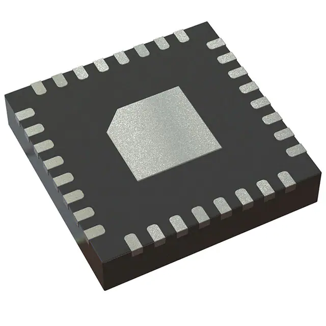
– 4-mm × 4-mm RSM VQFN32 (10 GPIOs)
– 5-mm × 5-mm RHB VQFN32 (15 GPIOs)
– 7-mm × 7-mm RGZ VQFN48 (31 GPIOs)
• Peripherals
– All Digital Peripheral Pins Can Be Routed to
Any GPIO
– Four General-Purpose Timer Modules
(Eight 16-Bit or Four 32-Bit Timers, PWM Each)
– 12-Bit ADC, 200-ksamples/s, 8-Channel Analog
MUX
– Continuous Time Comparator
– Ultra-Low-Power Analog Comparator
– Programmable Current Source
– UART
– 2× SSI (SPI, MICROWIRE, TI)
– I2C
– I2S
– Real-Time Clock (RTC)
– AES-128 Security Module
– True Random Number Generator (TRNG)
– 10, 14, 15, or 31 GPIOs, Depending on
Package Option
– Support for Eight Capacitive-Sensing Buttons
– Integrated Temperature Sensor
• External System
– On-Chip internal DC-DC Converter
– Very Few External Components
– Seamless Integration With the SimpleLink™
CC2590 and CC2592 Range Extenders
– Pin Compatible With the SimpleLink CC13xx in
4-mm × 4-mm and 5-mm × 5-mm VQFN
Packages
• Low Power
– Wide Supply Voltage Range
– Normal Operation: 1.8 to 3.8 V
– External Regulator Mode: 1.7 to 1.95 V
– Active-Mode RX: 5.9 mA
– Active-Mode TX at 0 dBm: 6.1 mA
– Active-Mode TX at +5 dBm: 9.1 mA
– Active-Mode MCU: 61 µA/MHz
– Active-Mode MCU: 48.5 CoreMark/mA
– Active-Mode Sensor Controller:
0.4mA + 8.2 µA/MHz
– Standby: 1.1 µA (RTC Running and RAM/CPU
Retention)
– Shutdown: 100 nA (Wake Up on External
Events)
• RF Section
– 2.4-GHz RF Transceiver Compatible With
Bluetooth low energy (BLE) 4.2 and 5
Specifications
– Excellent Receiver Sensitivity (–97 dBm for
BLE), Selectivity, and Blocking Performance
– Link Budget of 102 dB for BLE
– Programmable Output Power up to +5 dBm
– Single-Ended or Differential RF Interface
– Suitable for Systems Targeting Compliance With
Worldwide Radio Frequency Regulations
– ETSI EN 300 328 (Europe)
– EN 300 440 Class 2 (Europe)
– FCC CFR47 Part 15 (US)
– ARIB STD-T66 (Japan)
• Tools and Development Environment
– Full-Feature Development Kits
– Multiple Reference Designs
– SmartRF™ Tools Portfolio
– Sensor Controller Studio
– IAR Embedded Workbench® for ARM
– Code Composer Studio™
– CCS Cloud
1
An IMPORTANT NOTICE at the end of this data sheet addresses availability, warranty, changes, use in safety-critical applications,
intellectual property matters and other important disclaimers. PRODUCTION DATA.
�CC2640R2F
SWRS204A – DECEMBER 2016 – REVISED JANUARY 2017
1.2
•
•
•
www.ti.com
Applications
Home and Building Automation
– Connected Appliances
– Lighting
– Locks
– Gateways
– Security Systems
Industrial
– Logistics
– Production and Manufacturing Automation
– Asset Tracking and Management
– HMI and Remote Display
– Access Control
Retail
– Beacons
– Advertising
– ESL and Price Tags
– Point of Sales and Payment Systems
1.3
•
•
•
Health and Medical
– Thermometers
– SpO2
– Blood Glucose and Pressure Meters
– Weight Scales
– Hearing Aids
Sports and Fitness
– Activity Monitors and Fitness Trackers
– Heart Rate Monitors
– Running and Biking Sensors
– Sports Watches
– Gym Equipment
– Team Sports Equipment
HID
– Voice Remote Controls
– Gaming
– Keyboards and Mice
Description
The CC2640R2F device is a wireless microcontroller (MCU) targeting Bluetooth® 4.2 and Bluetooth 5 lowenergy applications.
The device is a member of the SimpleLink™ ultra-low power CC26xx family of cost-effective, 2.4-GHz RF
devices. Very low active RF and MCU current and low-power mode current consumption provide excellent
battery lifetime and allow for operation on small coin cell batteries and in energy-harvesting applications.
The SimpleLink Bluetooth low energy CC2640R2F device contains a 32-bit ARM® Cortex®-M3 core that
runs at 48 MHz as the main processor and a rich peripheral feature set that includes a unique ultra-low
power sensor controller. This sensor controller is ideal for interfacing external sensors and for collecting
analog and digital data autonomously while the rest of the system is in sleep mode. Thus, the CC2640R2F
device is great for a wide range of applications where long battery lifetime, small form factor, and ease of
use is important.
The power and clock management and radio systems of the CC2640R2F wireless MCU require specific
configuration and handling by software to operate correctly, which has been implemented in the TI-RTOS.
TI recommends using this software framework for all application development on the device. The complete
TI-RTOS and device drivers are offered in source code free of charge from www.ti.com.
Bluetooth low energy controller and host libraries are embedded in ROM and run partly on an ARM®
Cortex®-M0 processor. This architecture improves overall system performance and power consumption
and frees up significant amounts of flash memory for the application.
The Bluetooth stack is available free of charge from www.ti.com.
Device Information (1)
(1)
2
PART NUMBER
PACKAGE
BODY SIZE (NOM)
CC2640R2FRGZ
VQFN (48)
7.00 mm × 7.00 mm
CC2640R2FRHB
VQFN (32)
5.00 mm × 5.00 mm
CC2640R2FRSM
VQFN (32)
4.00 mm × 4.00 mm
CC2640R2FYFV
DSBGA (34)
2.70 mm × 2.70 mm
For more information, see Section 9.
Device Overview
Copyright © 2016–2017, Texas Instruments Incorporated
Submit Documentation Feedback
Product Folder Links: CC2640R2F
�CC2640R2F
www.ti.com
1.4
SWRS204A – DECEMBER 2016 – REVISED JANUARY 2017
Functional Block Diagram
Figure 1-1 shows a block diagram for the CC2640R2F device.
SimpleLink CC26xx Wireless MCU
RF Core
cJTAG
Main CPU:
ROM
ADC
ADC
ARM
Cortex-M3
128-KB
Flash
8-KB
cache
Up to 48 MHz
61 µA/MHz
20-KB
SRAM
Digital PLL
DSP modem
ARM
Cortex-M0
ROM
General Peripherals / Modules
2
4-KB
SRAM
Sensor Controller
4× 32-bit Timers
I C
Sensor Controller Engine
UART
2× SSI (SPI, µW, TI)
12-bit ADC, 200 ks/s
I2S
Watchdog Timer
2× Comparator
10 / 14 / 15 / 31 GPIOs
TRNG
2
SPI-I C Digital Sensor IF
AES
Temp. / Batt. Monitor
Constant Current Source
32 ch. µDMA
RTC
Time-to-digital Converter
2-KB SRAM
DC-DC Converter
Copyright © 2016, Texas Instruments Incorporated
Figure 1-1. Block Diagram
Device Overview
Copyright © 2016–2017, Texas Instruments Incorporated
Submit Documentation Feedback
Product Folder Links: CC2640R2F
3
�CC2640R2F
SWRS204A – DECEMBER 2016 – REVISED JANUARY 2017
www.ti.com
Table of Contents
1
Device Overview ......................................... 1
1.1
Features .............................................. 1
1.2
Applications ........................................... 2
1.3
Description ............................................ 2
1.4
Functional Block Diagram ............................ 3
2
3
Revision History ......................................... 4
Device Comparison ..................................... 5
4
Terminal Configuration and Functions .............. 6
3.1
4.1
4.2
4.3
4.4
4.5
4.6
4.7
6
........................ 6
Signal Descriptions – RGZ Package ................. 7
Pin Diagram – RHB Package ........................ 9
Signal Descriptions – RHB Package ................ 10
Pin Diagram – RGZ Package
Pin Diagram – YFV (Chip Scale, DSBGA) Package 11
Signal Descriptions – YFV (Chip Scale, DSBGA)
Package ............................................. 11
Pin Diagram – RSM Package ....................... 13
...............
Specifications ...........................................
5.1
Absolute Maximum Ratings .........................
5.2
ESD Ratings ........................................
5.3
Recommended Operating Conditions ...............
5.4
Power Consumption Summary......................
5.5
General Characteristics .............................
5.6
125-kbps Coded (Bluetooth 5) – RX ................
5.7
125-kbps Coded (Bluetooth 5) – TX ................
5.8
500-kbps Coded (Bluetooth 5) – RX ................
5.9
500-kbps Coded (Bluetooth 5) – TX ................
5.10 1-Mbps GFSK (Bluetooth low energy) – RX ........
5.11 1-Mbps GFSK (Bluetooth low energy) – TX ........
5.12 2-Mbps GFSK (Bluetooth 5) – RX ..................
5.13 2-Mbps GFSK (Bluetooth 5) – TX ...................
5.14 24-MHz Crystal Oscillator (XOSC_HF) .............
5.15 32.768-kHz Crystal Oscillator (XOSC_LF) ..........
5.16 48-MHz RC Oscillator (RCOSC_HF) ...............
5.17 32-kHz RC Oscillator (RCOSC_LF).................
5.18 ADC Characteristics.................................
5.19 Temperature Sensor ................................
5.20 Battery Monitor ......................................
5.21 Continuous Time Comparator .......................
5.22 Low-Power Clocked Comparator ...................
4.8
5
Related Products ..................................... 5
Signal Descriptions – RSM Package
14
15
15
15
7
15
16
.....................
................
5.25 DC Characteristics ..................................
5.26 Thermal Resistance Characteristics ................
5.27 Timing Requirements ...............................
5.28 Switching Characteristics ...........................
5.29 Typical Characteristics ..............................
Detailed Description ...................................
6.1
Overview ............................................
6.2
Functional Block Diagram ...........................
6.3
Main CPU ...........................................
6.4
RF Core .............................................
6.5
Sensor Controller ...................................
6.6
Memory ..............................................
6.7
Debug ...............................................
6.8
Power Management .................................
6.9
Clock Systems ......................................
6.10 General Peripherals and Modules ..................
6.11 Voltage Supply Domains ............................
6.12 System Architecture .................................
Application, Implementation, and Layout .........
7.1
Application Information ..............................
5.23
Programmable Current Source
24
5.24
Synchronous Serial Interface (SSI)
25
7.2
16
7.3
17
18
18
8
26
27
28
28
29
33
33
33
34
34
35
36
36
37
38
38
39
39
40
40
5 × 5 External Differential (5XD) Application Circuit
...................................................... 42
4 × 4 External Single-ended (4XS) Application
Circuit ............................................... 44
Device and Documentation Support ............... 46
19
8.1
Device Nomenclature ............................... 46
19
8.2
Tools and Software
20
8.3
Documentation Support ............................. 48
20
8.4
Texas Instruments Low-Power RF Website
21
8.5
Low-Power RF eNewsletter ......................... 48
21
8.6
Community Resources .............................. 48
22
8.7
Additional Information ............................... 49
22
8.8
Trademarks.......................................... 49
22
8.9
Electrostatic Discharge Caution ..................... 49
22
8.10
Export Control Notice
8.11
23
24
24
24
9
.................................
........
...............................
Glossary .............................................
47
48
49
49
Mechanical, Packaging, and Orderable
Information .............................................. 49
9.1
Packaging Information
..............................
49
2 Revision History
NOTE: Page numbers for previous revisions may differ from page numbers in the current version.
Changes from December 6, 2016 to January 13, 2017
•
4
Changed Section 5.2
Page
...............................................................................................................
Revision History
15
Copyright © 2016–2017, Texas Instruments Incorporated
Submit Documentation Feedback
Product Folder Links: CC2640R2F
�CC2640R2F
www.ti.com
SWRS204A – DECEMBER 2016 – REVISED JANUARY 2017
3 Device Comparison
Table 3-1. Device Family Overview
Device
PHY Support
Flash (KB)
RAM (KB)
GPIO
Package (1)
CC2640R2Fxxx (2)
Bluetooth low energy (Normal, High
Speed, Long Range)
128
20
31, 15, 14, 10
RGZ, RHB, YFV, RSM
CC2640F128xxx
Bluetooth low energy (Normal)
128
20
31, 15, 10
RGZ, RHB, RSM
CC2650F128xxx
Multi-Protocol (3)
128
20
31, 15, 10
RGZ, RHB, RSM
CC2630F128xxx
IEEE 802.15.4 (/6LoWPAN)
128
20
31, 15, 10
RGZ, RHB, RSM
CC2620F128xxx
IEEE 802.15.4 (RF4CE)
128
20
31, 10
RGZ, RSM
(1)
(2)
(3)
Package designator replaces the xxx in device name to form a complete device name, RGZ is 7-mm × 7-mm VQFN48, RHB is
5-mm × 5-mm VQFN32, RSM is 4-mm × 4-mm VQFN32, and YFV is 2.7-mm × 2.7-mm DSBGA.
CC2640R2Fxxx devices contain Bluetooth 4.2 low energy Host & Controller libraries in ROM, leaving more of the 128KB flash available
for the customer application when used with supported BLE-Stack software protocol stack releases. Actual use of ROM and flash by the
protocol stack may vary depending on device software configuration. See www.ti.com and Table 3-2 for more details.
The CC2650 device supports all PHYs and can be reflashed to run all the supported standards.
Table 3-2. Typical (1) Flash Memory Available for Customer Applications
Simple BLE Peripheral (BT 4.0) (2)
Device
CC2640R2Fxxx
(4)
CC2640F128xxx, CC2650F128xxx
(1)
(2)
(3)
(4)
3.1
Simple BLE Peripheral (BT 4.2) (2)
83 KB
80 KB
41 KB
31 KB
(3)
Actual use of ROM and flash by the protocol stack will vary depending on device software configuration. The values in this table are
provided as guidance only.
Application example with two services (GAP and Simple Profile). Compiled using IAR.
BT4.2 configuration including Secure Pairing, Privacy 1.2, and Data Length Extension
BLE applications running on the CC2640R2F device make use of up to 115 KB of system ROM and up to 32 KB of RF Core ROM in
order to minimize the flash usage. The maximum amount of nonvolatile memory available for BLE applications on CC2640R2F is thus
275 KB (128-KB flash + 147-KB ROM).
Related Products
TI's Wireless Connectivity
The wireless connectivity portfolio offers a wide selection of low-power RF solutions suitable
for a broad range of applications. The offerings range from fully customized solutions to turn
key offerings with pre-certified hardware and software (protocol).
TI's SimpleLink™ Sub-1 GHz Wireless MCUs
Long-range, low-power wireless connectivity solutions are offered in a wide range of
Sub-1 GHz ISM bands.
Companion ProductsCompanion Products
Review products that are frequently purchased or used in conjunction with this product.
SimpleLink™ CC2640R2 Wireless MCU LaunchPad™ Development Kit
The CC2640R2 LaunchPad ™ development kit brings easy Bluetooth® low energy (BLE)
connection to the LaunchPad ecosystem with the SimpleLink ultra-low power CC26xx family
of devices. Compared to the CC2650 LaunchPad, the CC2640R2 LaunchPad provides the
following:
• More free flash memory for the user application in the CC2640R2 wireless MCU
• Out-of-the-box support for Bluetooth 4.2 specification
• 4× faster Over-the-Air download speed compared to Bluetooth 4.1
SimpleLink™ Bluetooth low energy/Multi-standard SensorTag
The new SensorTag IoT kit invites you to realize your cloud-connected product idea. The
new SensorTag now includes 10 low-power MEMS sensors in a tiny red package. And it is
expandable with DevPacks to make it easy to add your own sensors or actuators.
Reference Designs for CC2640
TI Designs Reference Design Library is a robust reference design library spanning analog,
embedded processor and connectivity. Created by TI experts to help you jump-start your
system design, all TI Designs include schematic or block diagrams, BOMs, and design files
to speed your time to market. Search and download designs at ti.com/tidesigns.
Device Comparison
Copyright © 2016–2017, Texas Instruments Incorporated
Submit Documentation Feedback
Product Folder Links: CC2640R2F
5
�CC2640R2F
SWRS204A – DECEMBER 2016 – REVISED JANUARY 2017
www.ti.com
4 Terminal Configuration and Functions
25 JTAG_TCKC
26 DIO_16
27 DIO_17
28 DIO_18
29 DIO_19
30 DIO_20
31 DIO_21
32 DIO_22
33 DCDC_SW
34 VDDS_DCDC
35 RESET_N
Pin Diagram – RGZ Package
36 DIO_23
4.1
DIO_24 37
24 JTAG_TMSC
DIO_25 38
23 DCOUPL
DIO_26 39
22 VDDS3
DIO_27 40
21 DIO_15
DIO_28 41
20 DIO_14
DIO_29 42
19 DIO_13
DIO_30 43
18 DIO_12
VDDS 44
17 DIO_11
VDDR 45
16 DIO_10
X24M_N 46
15 DIO_9
X24M_P 47
14 DIO_8
13 VDDS2
6
7
8
9
DIO_1
DIO_2
DIO_3
DIO_4
DIO_7 12
5
DIO_0
DIO_6 11
4
DIO_5 10
3
X32K_Q2
2
RF_N
X32K_Q1
1
RF_P
VDDR_RF 48
Figure 4-1. RGZ Package
48-Pin VQFN
(7-mm × 7-mm) Pinout, 0.5-mm Pitch
I/O pins marked in Figure 4-1 in bold have high-drive capabilities; they are the following:
• Pin 10, DIO_5
• Pin 11, DIO_6
• Pin 12, DIO_7
• Pin 24, JTAG_TMSC
• Pin 26, DIO_16
• Pin 27, DIO_17
I/O pins marked in Figure 4-1 in italics have analog capabilities; they are the following:
• Pin 36, DIO_23
• Pin 37, DIO_24
• Pin 38, DIO_25
• Pin 39, DIO_26
• Pin 40, DIO_27
• Pin 41, DIO_28
• Pin 42, DIO_29
• Pin 43, DIO_30
6
Terminal Configuration and Functions
Copyright © 2016–2017, Texas Instruments Incorporated
Submit Documentation Feedback
Product Folder Links: CC2640R2F
�CC2640R2F
www.ti.com
4.2
SWRS204A – DECEMBER 2016 – REVISED JANUARY 2017
Signal Descriptions – RGZ Package
Table 4-1. Signal Descriptions – RGZ Package
NAME
NO.
TYPE
DESCRIPTION
DCDC_SW
33
Power
Output from internal DC-DC (1)
DCOUPL
23
Power
1.27-V regulated digital-supply decoupling capacitor (2)
DIO_0
5
Digital I/O
GPIO, Sensor Controller
DIO_1
6
Digital I/O
GPIO, Sensor Controller
DIO_2
7
Digital I/O
GPIO, Sensor Controller
DIO_3
8
Digital I/O
GPIO, Sensor Controller
DIO_4
9
Digital I/O
GPIO, Sensor Controller
DIO_5
10
Digital I/O
GPIO, Sensor Controller, high-drive capability
DIO_6
11
Digital I/O
GPIO, Sensor Controller, high-drive capability
DIO_7
12
Digital I/O
GPIO, Sensor Controller, high-drive capability
DIO_8
14
Digital I/O
GPIO
DIO_9
15
Digital I/O
GPIO
DIO_10
16
Digital I/O
GPIO
DIO_11
17
Digital I/O
GPIO
DIO_12
18
Digital I/O
GPIO
DIO_13
19
Digital I/O
GPIO
DIO_14
20
Digital I/O
GPIO
DIO_15
21
Digital I/O
GPIO
DIO_16
26
Digital I/O
GPIO, JTAG_TDO, high-drive capability
DIO_17
27
Digital I/O
GPIO, JTAG_TDI, high-drive capability
DIO_18
28
Digital I/O
GPIO
DIO_19
29
Digital I/O
GPIO
DIO_20
30
Digital I/O
GPIO
DIO_21
31
Digital I/O
GPIO
DIO_22
32
Digital I/O
GPIO
DIO_23
36
Digital/Analog I/O
GPIO, Sensor Controller, Analog
DIO_24
37
Digital/Analog I/O
GPIO, Sensor Controller, Analog
DIO_25
38
Digital/Analog I/O
GPIO, Sensor Controller, Analog
DIO_26
39
Digital/Analog I/O
GPIO, Sensor Controller, Analog
DIO_27
40
Digital/Analog I/O
GPIO, Sensor Controller, Analog
DIO_28
41
Digital/Analog I/O
GPIO, Sensor Controller, Analog
DIO_29
42
Digital/Analog I/O
GPIO, Sensor Controller, Analog
DIO_30
43
Digital/Analog I/O
GPIO, Sensor Controller, Analog
JTAG_TMSC
24
Digital I/O
JTAG TMSC, high-drive capability
JTAG_TCKC
25
Digital I/O
JTAG TCKC
RESET_N
35
Digital input
RF_P
1
RF I/O
Positive RF input signal to LNA during RX
Positive RF output signal to PA during TX
RF_N
2
RF I/O
Negative RF input signal to LNA during RX
Negative RF output signal to PA during TX
VDDR
45
Power
1.7-V to 1.95-V supply, typically connect to output of internal DC-DC (2) (3)
VDDR_RF
48
Power
1.7-V to 1.95-V supply, typically connect to output of internal DC-DC (2) (4)
VDDS
44
Power
1.8-V to 3.8-V main chip supply (1)
(1)
(2)
(3)
(4)
Reset, active-low. No internal pullup.
For more details, see the technical reference manual (listed in Section 8.3).
Do not supply external circuitry from this pin.
If internal DC-DC is not used, this pin is supplied internally from the main LDO.
If internal DC-DC is not used, this pin must be connected to VDDR for supply from the main LDO.
Terminal Configuration and Functions
Copyright © 2016–2017, Texas Instruments Incorporated
Submit Documentation Feedback
Product Folder Links: CC2640R2F
7
�CC2640R2F
SWRS204A – DECEMBER 2016 – REVISED JANUARY 2017
www.ti.com
Table 4-1. Signal Descriptions – RGZ Package (continued)
NAME
NO.
TYPE
DESCRIPTION
VDDS2
13
Power
1.8-V to 3.8-V DIO supply (1)
VDDS3
22
Power
1.8-V to 3.8-V DIO supply (1)
VDDS_DCDC
34
Power
1.8-V to 3.8-V DC-DC supply
X32K_Q1
3
Analog I/O
32-kHz crystal oscillator pin 1
X32K_Q2
4
Analog I/O
32-kHz crystal oscillator pin 2
X24M_N
46
Analog I/O
24-MHz crystal oscillator pin 1
X24M_P
47
Analog I/O
24-MHz crystal oscillator pin 2
EGP
8
Power
Ground – Exposed Ground Pad
Terminal Configuration and Functions
Copyright © 2016–2017, Texas Instruments Incorporated
Submit Documentation Feedback
Product Folder Links: CC2640R2F
�CC2640R2F
www.ti.com
17 DCDC_SW
18 VDDS_DCDC
19 RESET_N
20 DIO_7
21 DIO_8
22 DIO_9
23 DIO_10
Pin Diagram – RHB Package
24 DIO_11
4.3
SWRS204A – DECEMBER 2016 – REVISED JANUARY 2017
DIO_12 25
16 DIO_6
DIO_13 26
15 DIO_5
DIO_14 27
14 JTAG_TCKC
VDDS 28
13 JTAG_TMSC
VDDR 29
12 DCOUPL
X24M_N 30
11 VDDS2
X24M_P 31
10 DIO_4
1
2
3
4
5
6
7
8
RF_N
RX_TX
X32K_Q1
X32K_Q2
DIO_0
DIO_1
DIO_2
9
RF_P
VDDR_RF 32
DIO_3
Figure 4-2. RHB Package
32-Pin VQFN
(5-mm × 5-mm) Pinout, 0.5-mm Pitch
I/O pins marked in Figure 4-2 in bold have high-drive capabilities; they are the following:
• Pin 8, DIO_2
• Pin 9, DIO_3
• Pin 10, DIO_4
• Pin 13, JTAG_TMSC
• Pin 15, DIO_5
• Pin 16, DIO_6
I/O pins marked in Figure 4-2 in italics have analog capabilities; they are the following:
• Pin 20, DIO_7
• Pin 21, DIO_8
• Pin 22, DIO_9
• Pin 23, DIO_10
• Pin 24, DIO_11
• Pin 25, DIO_12
• Pin 26, DIO_13
• Pin 27, DIO_14
Terminal Configuration and Functions
Copyright © 2016–2017, Texas Instruments Incorporated
Submit Documentation Feedback
Product Folder Links: CC2640R2F
9
�CC2640R2F
SWRS204A – DECEMBER 2016 – REVISED JANUARY 2017
4.4
www.ti.com
Signal Descriptions – RHB Package
Table 4-2. Signal Descriptions – RHB Package
NAME
NO.
TYPE
DESCRIPTION
DCDC_SW
17
Power
Output from internal DC-DC (1)
DCOUPL
12
Power
1.27-V regulated digital-supply decoupling (2)
DIO_0
6
Digital I/O
GPIO, Sensor Controller
DIO_1
7
Digital I/O
GPIO, Sensor Controller
DIO_2
8
Digital I/O
GPIO, Sensor Controller, high-drive capability
DIO_3
9
Digital I/O
GPIO, Sensor Controller, high-drive capability
DIO_4
10
Digital I/O
GPIO, Sensor Controller, high-drive capability
DIO_5
15
Digital I/O
GPIO, High drive capability, JTAG_TDO
DIO_6
16
Digital I/O
GPIO, High drive capability, JTAG_TDI
DIO_7
20
Digital/Analog I/O
GPIO, Sensor Controller, Analog
DIO_8
21
Digital/Analog I/O
GPIO, Sensor Controller, Analog
DIO_9
22
Digital/Analog I/O
GPIO, Sensor Controller, Analog
DIO_10
23
Digital/Analog I/O
GPIO, Sensor Controller, Analog
DIO_11
24
Digital/Analog I/O
GPIO, Sensor Controller, Analog
DIO_12
25
Digital/Analog I/O
GPIO, Sensor Controller, Analog
DIO_13
26
Digital/Analog I/O
GPIO, Sensor Controller, Analog
DIO_14
27
Digital/Analog I/O
GPIO, Sensor Controller, Analog
JTAG_TMSC
13
Digital I/O
JTAG TMSC, high-drive capability
JTAG_TCKC
14
Digital I/O
JTAG TCKC
RESET_N
19
Digital input
RF_N
2
RF I/O
Negative RF input signal to LNA during RX
Negative RF output signal to PA during TX
RF_P
1
RF I/O
Positive RF input signal to LNA during RX
Positive RF output signal to PA during TX
RX_TX
3
RF I/O
Optional bias pin for the RF LNA
VDDR
29
Power
1.7-V to 1.95-V supply, typically connect to output of internal DC-DC (3) (2)
VDDR_RF
32
Power
1.7-V to 1.95-V supply, typically connect to output of internal DC-DC (2) (4)
VDDS
28
Power
1.8-V to 3.8-V main chip supply (1)
VDDS2
11
Power
1.8-V to 3.8-V GPIO supply (1)
VDDS_DCDC
18
Power
1.8-V to 3.8-V DC-DC supply
X32K_Q1
4
Analog I/O
32-kHz crystal oscillator pin 1
X32K_Q2
5
Analog I/O
32-kHz crystal oscillator pin 2
X24M_N
30
Analog I/O
24-MHz crystal oscillator pin 1
X24M_P
31
Analog I/O
24-MHz crystal oscillator pin 2
EGP
(1)
(2)
(3)
(4)
10
Power
Reset, active-low. No internal pullup.
Ground – Exposed Ground Pad
See technical reference manual (listed in Section 8.3) for more details.
Do not supply external circuitry from this pin.
If internal DC-DC is not used, this pin is supplied internally from the main LDO.
If internal DC-DC is not used, this pin must be connected to VDDR for supply from the main LDO.
Terminal Configuration and Functions
Copyright © 2016–2017, Texas Instruments Incorporated
Submit Documentation Feedback
Product Folder Links: CC2640R2F
�CC2640R2F
www.ti.com
4.5
SWRS204A – DECEMBER 2016 – REVISED JANUARY 2017
Pin Diagram – YFV (Chip Scale, DSBGA) Package
A1
A2
A3
A4
B1
B2
B3
B4
B5
B6
C1
C2
C3
C4
C5
C6
D1
D2
D3
D4
D5
D6
E1
E2
E3
E4
E5
E6
F1
F2
F3
F4
F5
F6
Figure 4-3. YFV (2.7-mm × 2.7-mm) Pinout, Top View
4.6
Signal Descriptions – YFV (Chip Scale, DSBGA) Package
Table 4-3. Signal Descriptions – YFV Package
NAME
NO.
TYPE
DESCRIPTION
DCDC_SW
D1
Power
Output from internal DC-DC (1)
DCOUPL
F3
Power
1.27-V regulated digital-supply decoupling (2)
DIO_0
C5
Digital I/O
GPIO, Sensor Controller
DIO_1
F6
Digital I/O
GPIO, Sensor Controller
DIO_2
D5
Digital I/O
GPIO, Sensor Controller, high-drive capability
DIO_3
E5
Digital I/O
GPIO, Sensor Controller, high-drive capability
DIO_4
F5
Digital I/O
GPIO, Sensor Controller, high-drive capability
DIO_5
E3
Digital I/O
GPIO, High-drive capability, JTAG_TDO
GPIO, High-drive capability, JTAG_TDI
DIO_6
F1
Digital I/O
DIO_7
D2
Digital/Analog I/O
GPIO, Sensor Controller, Analog
DIO_8
D3
Digital/Analog I/O
GPIO, Sensor Controller, Analog
DIO_9
A1
Digital/Analog I/O
GPIO, Sensor Controller, Analog
DIO_10
C2
Digital/Analog I/O
GPIO, Sensor Controller, Analog
DIO_11
B2
Digital/Analog I/O
GPIO, Sensor Controller, Analog
DIO_12
D4
Digital/Analog I/O
GPIO, Sensor Controller, Analog
DIO_13
B3
Digital/Analog I/O
GPIO, Sensor Controller, Analog
JTAG_TMSC
E4
Digital I/O
JTAG TMSC, high-drive capability
JTAG_TCKC
F2
Digital I/O
JTAG TCKC
RESET_N
E2
Digital input
RF_N
B6
RF I/O
Negative RF input signal to LNA during RX
Negative RF output signal to PA during TX
RF_P
B5
RF I/O
Positive RF input signal to LNA during RX
Positive RF output signal to PA during TX
(1)
(2)
Reset, active-low. No internal pullup.
For more details, see the technical reference manual (listed in Section 8.3).
Do not supply external circuitry from this pin.
Terminal Configuration and Functions
Copyright © 2016–2017, Texas Instruments Incorporated
Submit Documentation Feedback
Product Folder Links: CC2640R2F
11
�CC2640R2F
SWRS204A – DECEMBER 2016 – REVISED JANUARY 2017
www.ti.com
Table 4-3. Signal Descriptions – YFV Package (continued)
NAME
NO.
TYPE
DESCRIPTION
VDDR
A3
Power
1.7-V to 1.95-V supply, typically connect to output of internal DC-DC (3) (2)
VDDR_RF
B4
Power
1.7-V to 1.95-V supply, typically connect to output of internal DC-DC (4) (2)
VDDS
A2
Power
1.8-V to 3.8-V main chip supply (1)
VDDS2
F4
Power
1.8-V to 3.8-V GPIO supply (1)
VDDS_DCDC
C1
Power
1.8-V to 3.8-V DC-DC supply
X32K_Q1
D6
Analog I/O
32-kHz crystal oscillator pin 1
X32K_Q2
E6
Analog I/O
32-kHz crystal oscillator pin 2
X24M_N
C3
Analog I/O
24-MHz crystal oscillator pin 1
X24M_P
C4
Analog I/O
24-MHz crystal oscillator pin 2
A4, B1, C6,
E1
Power
GND
(3)
(4)
12
Ground
If internal DC-DC is not used, this pin is supplied internally from the main LDO.
If internal DC-DC is not used, this pin must be connected to VDDR for supply from the main LDO.
Terminal Configuration and Functions
Copyright © 2016–2017, Texas Instruments Incorporated
Submit Documentation Feedback
Product Folder Links: CC2640R2F
�CC2640R2F
www.ti.com
17 VSS
18 DCDC_SW
19 VDDS_DCDC
20 VSS
21 RESET_N
22 DIO_5
23 DIO_6
Pin Diagram – RSM Package
24 DIO_7
4.7
SWRS204A – DECEMBER 2016 – REVISED JANUARY 2017
DIO_8 25
16 DIO_4
DIO_9 26
15 DIO_3
VDDS 27
14 JTAG_TCKC
VDDR 28
13 JTAG_TMSC
VSS 29
12 DCOUPL
X24M_N 30
11 VDDS2
X24M_P 31
10 DIO_2
1
2
3
4
5
6
7
8
RF_N
VSS
RX_TX
X32K_Q1
X32K_Q2
VSS
DIO_0
9
RF_P
VDDR_RF 32
DIO_1
Figure 4-4. RSM Package
32-Pin VQFN
(4-mm × 4-mm) Pinout, 0.4-mm Pitch
I/O pins marked in Figure 4-4 in bold have high-drive capabilities; they are as follows:
• Pin 8, DIO_0
• Pin 9, DIO_1
• Pin 10, DIO_2
• Pin 13, JTAG_TMSC
• Pin 15, DIO_3
• Pin 16, DIO_4
I/O pins marked in Figure 4-4 in italics have analog capabilities; they are as follows:
• Pin 22, DIO_5
• Pin 23, DIO_6
• Pin 24, DIO_7
• Pin 25, DIO_8
• Pin 26, DIO_9
Terminal Configuration and Functions
Copyright © 2016–2017, Texas Instruments Incorporated
Submit Documentation Feedback
Product Folder Links: CC2640R2F
13
�CC2640R2F
SWRS204A – DECEMBER 2016 – REVISED JANUARY 2017
4.8
www.ti.com
Signal Descriptions – RSM Package
Table 4-4. Signal Descriptions – RSM Package
NAME
NO.
TYPE
DESCRIPTION
DCDC_SW
18
Power
Output from internal DC-DC. (1). Tie to ground for external regulator mode
(1.7-V to 1.95-V operation)
DCOUPL
12
Power
1.27-V regulated digital-supply decoupling capacitor (2)
DIO_0
8
Digital I/O
GPIO, Sensor Controller, high-drive capability
DIO_1
9
Digital I/O
GPIO, Sensor Controller, high-drive capability
DIO_2
10
Digital I/O
GPIO, Sensor Controller, high-drive capability
DIO_3
15
Digital I/O
GPIO, High-drive capability, JTAG_TDO
DIO_4
16
Digital I/O
GPIO, High-drive capability, JTAG_TDI
DIO_5
22
Digital/Analog I/O
GPIO, Sensor Controller, Analog
DIO_6
23
Digital/Analog I/O
GPIO, Sensor Controller, Analog
DIO_7
24
Digital/Analog I/O
GPIO, Sensor Controller, Analog
DIO_8
25
Digital/Analog I/O
GPIO, Sensor Controller, Analog
DIO_9
26
Digital/Analog I/O
GPIO, Sensor Controller, Analog
JTAG_TMSC
13
Digital I/O
JTAG TMSC
JTAG_TCKC
14
Digital I/O
JTAG TCKC
RESET_N
21
Digital Input
RF_N
2
RF I/O
Negative RF input signal to LNA during RX
Negative RF output signal to PA during TX
RF_P
1
RF I/O
Positive RF input signal to LNA during RX
Positive RF output signal to PA during TX
RX_TX
4
RF I/O
Optional bias pin for the RF LNA
VDDR
28
Power
1.7-V to 1.95-V supply, typically connect to output of internal DC-DC. (2) (3)
VDDR_RF
32
Power
1.7-V to 1.95-V supply, typically connect to output of internal DC-DC (2) (4)
VDDS
27
Power
1.8-V to 3.8-V main chip supply (1)
VDDS2
11
Power
1.8-V to 3.8-V GPIO supply (1)
VDDS_DCDC
19
Power
1.8-V to 3.8-V DC-DC supply. Tie to ground for external regulator mode
(1.7-V to 1.95-V operation).
3, 7, 17, 20,
29
Power
Ground
X32K_Q1
5
Analog I/O
32-kHz crystal oscillator pin 1
X32K_Q2
6
Analog I/O
32-kHz crystal oscillator pin 2
X24M_N
30
Analog I/O
24-MHz crystal oscillator pin 1
X24M_P
31
Analog I/O
24-MHz crystal oscillator pin 2
VSS
EGP
(1)
(2)
(3)
(4)
14
Power
Reset, active-low. No internal pullup.
Ground – Exposed Ground Pad
See technical reference manual (listed in Section 8.3) for more details.
Do not supply external circuitry from this pin.
If internal DC-DC is not used, this pin is supplied internally from the main LDO.
If internal DC-DC is not used, this pin must be connected to VDDR for supply from the main LDO.
Terminal Configuration and Functions
Copyright © 2016–2017, Texas Instruments Incorporated
Submit Documentation Feedback
Product Folder Links: CC2640R2F
�CC2640R2F
www.ti.com
SWRS204A – DECEMBER 2016 – REVISED JANUARY 2017
5 Specifications
5.1
Absolute Maximum Ratings
over operating free-air temperature range (unless otherwise noted) (1) (2)
MIN
MAX
Supply voltage (VDDS, VDDS2,
and VDDS3)
VDDR supplied by internal DC-DC regulator or
internal GLDO. VDDS_DCDC connected to VDDS on
PCB.
UNIT
–0.3
4.1
V
Supply voltage (VDDS (3) and
VDDR)
External regulator mode (VDDS and VDDR pins
connected on PCB)
–0.3
2.25
V
Voltage on any digital pin (4) (5)
–0.3
VDDSx + 0.3, max 4.1
V
Voltage on crystal oscillator pins, X32K_Q1, X32K_Q2, X24M_N and X24M_P
–0.3
VDDR + 0.3, max 2.25
V
Voltage scaling enabled
–0.3
VDDS
Voltage scaling disabled, internal reference
–0.3
1.49
Voltage scaling disabled, VDDS as reference
–0.3
VDDS / 2.9
Storage temperature
–40
150
Voltage on ADC input (Vin)
Input RF level
5
Tstg
(1)
(2)
(3)
(4)
(5)
°C
ESD Ratings
VALUE
VESD
VESD
5.3
dBm
All voltage values are with respect to ground, unless otherwise noted.
Stresses beyond those listed under Absolute Maximum Ratings may cause permanent damage to the device. These are stress ratings
only, and functional operation of the device at these or any other conditions beyond those indicated under Recommended Operating
Conditions is not implied. Exposure to absolute-maximum-rated conditions for extended periods may affect device reliability.
In external regulator mode, VDDS2 and VDDS3 must be at the same potential as VDDS.
Including analog-capable DIO.
Each pin is referenced to a specific VDDSx (VDDS, VDDS2 or VDDS3). For a pin-to-VDDS mapping table, see Table 6-3.
5.2
(1)
(2)
V
Electrostatic discharge
...
RSM, RHB, and RGZ packages
Electrostatic discharge
...
YFV package
Human body model (HBM), per
ANSI/ESDA/JEDEC JS001 (1)
Charged device model (CDM), per JESD22C101 (2)
Human body model (HBM), per
ANSI/ESDA/JEDEC JS001 (1)
Charged device model (CDM), per JESD22C101 (2)
All pins
±2500
RF pins
±750
Non-RF pins
±750
All pins
±1500
RF pins
±500
Non-RF pins
±500
UNIT
V
V
JEDEC document JEP155 states that 500-V HBM allows safe manufacturing with a standard ESD control process.
JEDEC document JEP157 states that 250-V CDM allows safe manufacturing with a standard ESD control process.
Recommended Operating Conditions
over operating free-air temperature range (unless otherwise noted)
MIN
MAX
–40
85
°C
1.7
1.95
V
1.8
3.8
V
VDDS < 2.7 V
1.8
3.8
V
VDDS ≥ 2.7 V
1.9
3.8
V
Ambient temperature
Operating supply
voltage (VDDS and
VDDR), external
regulator mode
For operation in 1.8-V systems
(VDDS and VDDR pins connected on PCB, internal DC-DC cannot be used)
Operating supply
voltage VDDS
Operating supply
voltages VDDS2 and
VDDS3
For operation in battery-powered and 3.3-V systems
(internal DC-DC can be used to minimize power consumption)
Operating supply
voltages VDDS2 and
VDDS3
Specifications
Copyright © 2016–2017, Texas Instruments Incorporated
Submit Documentation Feedback
Product Folder Links: CC2640R2F
UNIT
15
�CC2640R2F
SWRS204A – DECEMBER 2016 – REVISED JANUARY 2017
5.4
www.ti.com
Power Consumption Summary
Measured on the TI CC2650EM-5XD reference design with Tc = 25°C, VDDS = 3.0 V with internal DC-DC converter, unless
otherwise noted.
PARAMETER
Icore
Core current consumption
TEST CONDITIONS
MIN
TYP
Reset. RESET_N pin asserted or VDDS below
Power-on-Reset threshold
100
Shutdown. No clocks running, no retention
150
Standby. With RTC, CPU, RAM and (partial)
register retention. RCOSC_LF
1.1
Standby. With RTC, CPU, RAM and (partial)
register retention. XOSC_LF
1.3
Standby. With Cache, RTC, CPU, RAM and
(partial) register retention. RCOSC_LF
2.8
Standby. With Cache, RTC, CPU, RAM and
(partial) register retention. XOSC_LF
3.0
Idle. Supply Systems and RAM powered.
550
(1)
nA
µA
5.9
Radio RX (2)
6.1
(1)
6.1
Radio TX, 5-dBm output power (2)
9.1
Radio TX, 0-dBm output power
UNIT
1.45 mA +
31 µA/MHz
Active. Core running CoreMark
Radio RX
MAX
mA
Peripheral Current Consumption (Adds to core current Icore for each peripheral unit activated) (3)
Iperi
(1)
(2)
(3)
5.5
Peripheral power domain
Delta current with domain enabled
20
µA
Serial power domain
Delta current with domain enabled
13
µA
RF Core
Delta current with power domain enabled, clock
enabled, RF core idle
237
µA
µDMA
Delta current with clock enabled, module idle
130
µA
Timers
Delta current with clock enabled, module idle
113
µA
I2C
Delta current with clock enabled, module idle
12
µA
I2S
Delta current with clock enabled, module idle
36
µA
SSI
Delta current with clock enabled, module idle
93
µA
UART
Delta current with clock enabled, module idle
164
µA
Single-ended RF mode is optimized for size and power consumption. Measured on CC2650EM-4XS.
Differential RF mode is optimized for RF performance. Measured on CC2650EM-5XD.
Iperi is not supported in Standby or Shutdown.
General Characteristics
Tc = 25°C, VDDS = 3.0 V, unless otherwise noted.
PARAMETER
TEST CONDITIONS
MIN
TYP
MAX
UNIT
FLASH MEMORY
Supported flash erase cycles before
failure
100
k Cycles
Maximum number of write operations
per row before erase (1)
83
write
operations
Years at
105°C
Flash retention
105°C
11.4
Flash page/sector erase current
Average delta current
12.6
4
KB
Average delta current, 4 bytes at a time
8.15
mA
8
ms
8
µs
Flash page/sector size
Flash write current
Flash page/sector erase time (2)
Flash write time
(1)
(2)
16
(2)
4 bytes at a time
mA
Each row is 2048 bits (or 256 Bytes) wide.
This number is dependent on Flash aging and will increase over time and erase cycles.
Specifications
Copyright © 2016–2017, Texas Instruments Incorporated
Submit Documentation Feedback
Product Folder Links: CC2640R2F
�CC2640R2F
www.ti.com
5.6
SWRS204A – DECEMBER 2016 – REVISED JANUARY 2017
125-kbps Coded (Bluetooth 5) – RX
Measured on the TI CC2650EM-5XD reference design with Tc = 25°C, VDDS = 3.0 V, fRF = 2440 MHz, unless otherwise noted.
PARAMETER
TEST CONDITIONS
MIN
TYP
MAX
UNIT
Receiver sensitivity
Differential mode. Measured at the CC2650EM-5XD
SMA connector, BER = 10–3
–103
dBm
Receiver saturation
Differential mode. Measured at the CC2650EM-5XD
SMA connector, BER = 10–3
>5
dBm
Frequency error tolerance
Difference between the incoming carrier frequency
and the internally generated carrier frequency
–260
310
kHz
Data rate error tolerance
Difference between incoming data rate and the
internally generated data rate (37-byte packets)
–260
260
ppm
Data rate error tolerance
Difference between incoming data rate and the
internally generated data rate (255-byte packets)
–140
150
ppm
Co-channel rejection
(1)
Wanted signal at –79 dBm, modulated interferer in
channel, BER = 10–3
–3
dB
9 / 5 (2)
dB
Selectivity, ±1 MHz
(1)
Wanted signal at –79 dBm, modulated interferer at
±1 MHz, BER = 10–3
Selectivity, ±2 MHz
(1)
Wanted signal at –79 dBm, modulated interferer at
±2 MHz, Image frequency is at –2 MHz, BER = 10–3
43 / 32 (2)
dB
Selectivity, ±3 MHz
(1)
Wanted signal at –79 dBm, modulated interferer at
±3 MHz, BER = 10–3
47 / 42 (2)
dB
Selectivity, ±4 MHz
(1)
Wanted signal at –79 dBm, modulated interferer at
±4 MHz, BER = 10–3
46 / 47 (2)
dB
Selectivity, ±6 MHz
(1)
Wanted signal at –79 dBm, modulated interferer at
±6 MHz, BER = 10–3
49 / 46 (2)
dB
50 / 47 (2)
dB
32
dB
5 / 32 (2)
dB
>46
dB
30 MHz to 2000 MHz
–40
dBm
Out-of-band blocking
2003 MHz to 2399 MHz
–19
dBm
Out-of-band blocking
2484 MHz to 2997 MHz
–22
dBm
Intermodulation
Wanted signal at 2402 MHz, –76 dBm. Two
interferers at 2405 and 2408 MHz respectively, at
the given power level
–42
dBm
Alternate channel rejection, ±7 Wanted signal at –79 dBm, modulated interferer at ≥
MHz (1)
±7 MHz, BER = 10–3
Selectivity, image frequency (1)
Wanted signal at –79 dBm, modulated interferer at
image frequency, BER = 10–3
Selectivity, image frequency
±1 MHz (1)
Note that Image frequency + 1 MHz is the Cochannel –1 MHz. Wanted signal at –79 dBm,
modulated interferer at ±1 MHz from image
frequency, BER = 10–3
Blocker rejection, ±8 MHz and Wanted signal at –79 dBm, modulated interferer at
above (1)
±8 MHz and above, BER = 10–3
Out-of-band blocking
(1)
(2)
(3)
(3)
Numbers given as I/C dB.
X / Y, where X is +N MHz and Y is –N MHz.
Excluding one exception at Fwanted / 2, per Bluetooth Specification.
Specifications
Copyright © 2016–2017, Texas Instruments Incorporated
Submit Documentation Feedback
Product Folder Links: CC2640R2F
17
�CC2640R2F
SWRS204A – DECEMBER 2016 – REVISED JANUARY 2017
5.7
www.ti.com
125-kbps Coded (Bluetooth 5) – TX
Measured on the TI CC2650EM-5XD reference design with Tc = 25°C, VDDS = 3.0 V, fRF = 2440 MHz, unless otherwise noted.
PARAMETER
TEST CONDITIONS
MIN
TYP
MAX
UNIT
Output power, highest setting
Differential mode, delivered to a single-ended 50-Ω load
through a balun
5
dBm
Output power, highest setting
Measured on CC2650EM-4XS, delivered to a single-ended
50-Ω load
2
dBm
Output power, lowest setting
Delivered to a single-ended 50-Ω load through a balun
–21
dBm
f < 1 GHz, outside restricted bands
–43
dBm
f < 1 GHz, restricted bands ETSI
–65
dBm
f < 1 GHz, restricted bands FCC
–76
dBm
f > 1 GHz, including harmonics
–46
dBm
Spurious emission conducted
measurement (1)
(1)
5.8
Suitable for systems targeting compliance with worldwide radio-frequency regulations ETSI EN 300 328 and EN 300 440 Class 2
(Europe), FCC CFR47 Part 15 (US), and ARIB STD-T66 (Japan).
500-kbps Coded (Bluetooth 5) – RX
Measured on the TI CC2650EM-5XD reference design with Tc = 25°C, VDDS = 3.0 V, fRF = 2440 MHz, unless otherwise noted.
PARAMETER
TEST CONDITIONS
MIN
TYP
MAX
UNIT
Receiver sensitivity
Differential mode. Measured at the CC2650EM-5XD
SMA connector, BER = 10–3
–101
dBm
Receiver saturation
Differential mode. Measured at the CC2650EM-5XD
SMA connector, BER = 10–3
>5
dBm
Frequency error tolerance
Difference between the incoming carrier frequency
and the internally generated carrier frequency
–240
240
kHz
Data rate error tolerance
Difference between incoming data rate and the
internally generated data rate (37-byte packets)
–500
500
ppm
Data rate error tolerance
Difference between incoming data rate and the
internally generated data rate (255-byte packets)
–310
330
ppm
Co-channel rejection
(1)
Wanted signal at –72 dBm, modulated interferer in
channel, BER = 10–3
–5
dB
9 / 5 (2)
dB
Selectivity, ±1 MHz
(1)
Wanted signal at –72 dBm, modulated interferer at
±1 MHz, BER = 10–3
Selectivity, ±2 MHz
(1)
Wanted signal at –72 dBm, modulated interferer at
±2 MHz, Image frequency is at –2 MHz, BER = 10–3
41 / 31 (2)
dB
Selectivity, ±3 MHz
(1)
Wanted signal at –72 dBm, modulated interferer at
±3 MHz, BER = 10–3
44 / 41 (2)
dB
Selectivity, ±4 MHz
(1)
Wanted signal at –72 dBm, modulated interferer at
±4 MHz, BER = 10–3
44 / 44 (2)
dB
Selectivity, ±6 MHz
(1)
Wanted signal at –72 dBm, modulated interferer at
±6 MHz, BER = 10–3
44 / 44 (2)
dB
Alternate channel rejection,
±7 MHz (1)
Wanted signal at –72 dBm, modulated interferer at
≥ ±7 MHz, BER = 10–3
44 / 44 (2)
dB
Selectivity, image frequency (1)
Wanted signal at –72 dBm, modulated interferer at
image frequency, BER = 10–3
31
dB
Selectivity, image frequency
±1 MHz (1)
Note that Image frequency + 1 MHz is the Cochannel –1 MHz. Wanted signal at –72 dBm,
modulated interferer at ±1 MHz from image
frequency, BER = 10–3
5 / 41 (2)
dB
44
dB
30 MHz to 2000 MHz
–35
dBm
Out-of-band blocking
2003 MHz to 2399 MHz
–19
dBm
Out-of-band blocking
2484 MHz to 2997 MHz
–19
dBm
Blocker rejection, ±8 MHz and Wanted signal at –72 dBm, modulated interferer at
above (1)
±8 MHz and above, BER = 10–3
Out-of-band blocking
(1)
(2)
(3)
18
(3)
Numbers given as I/C dB.
X / Y, where X is +N MHz and Y is –N MHz.
Excluding one exception at Fwanted / 2, per Bluetooth Specification.
Specifications
Copyright © 2016–2017, Texas Instruments Incorporated
Submit Documentation Feedback
Product Folder Links: CC2640R2F
�CC2640R2F
www.ti.com
SWRS204A – DECEMBER 2016 – REVISED JANUARY 2017
500-kbps Coded (Bluetooth 5) – RX (continued)
Measured on the TI CC2650EM-5XD reference design with Tc = 25°C, VDDS = 3.0 V, fRF = 2440 MHz, unless otherwise noted.
PARAMETER
Intermodulation
5.9
TEST CONDITIONS
MIN
TYP
Wanted signal at 2402 MHz, –69 dBm. Two
interferers at 2405 and 2408 MHz respectively, at
the given power level
MAX
–37
UNIT
dBm
500-kbps Coded (Bluetooth 5) – TX
Measured on the TI CC2650EM-5XD reference design with Tc = 25°C, VDDS = 3.0 V, fRF = 2440 MHz, unless otherwise noted.
PARAMETER
TEST CONDITIONS
MIN
TYP
MAX
UNIT
Output power, highest setting
Differential mode, delivered to a single-ended 50-Ω load
through a balun
5
dBm
Output power, highest setting
Measured on CC2650EM-4XS, delivered to a single-ended
50-Ω load
2
dBm
Output power, lowest setting
Delivered to a single-ended 50-Ω load through a balun
–21
dBm
f < 1 GHz, outside restricted bands
–43
dBm
f < 1 GHz, restricted bands ETSI
–65
dBm
f < 1 GHz, restricted bands FCC
–76
dBm
f > 1 GHz, including harmonics
–46
dBm
Spurious emission conducted
measurement (1)
(1)
Suitable for systems targeting compliance with worldwide radio-frequency regulations ETSI EN 300 328 and EN 300 440 Class 2
(Europe), FCC CFR47 Part 15 (US), and ARIB STD-T66 (Japan).
5.10 1-Mbps GFSK (Bluetooth low energy) – RX
Measured on the TI CC2650EM-5XD reference design with Tc = 25°C, VDDS = 3.0 V, fRF = 2440 MHz, unless otherwise noted.
PARAMETER
TEST CONDITIONS
MIN
TYP
MAX
UNIT
Receiver sensitivity
Differential mode. Measured at the CC2650EM-5XD
SMA connector, BER = 10–3
–97
dBm
Receiver sensitivity
Single-ended mode. Measured on CC2650EM-4XS,
at the SMA connector, BER = 10–3
–96
dBm
Receiver saturation
Differential mode. Measured at the CC2650EM-5XD
SMA connector, BER = 10–3
4
dBm
Receiver saturation
Single-ended mode. Measured on CC2650EM-4XS,
at the SMA connector, BER = 10–3
0
dBm
Frequency error tolerance
Difference between the incoming carrier frequency
and the internally generated carrier frequency
–350
350
kHz
Data rate error tolerance
Difference between incoming data rate and the
internally generated data rate
–750
750
ppm
Co-channel rejection (1)
Wanted signal at –67 dBm, modulated interferer in
channel, BER = 10–3
–6
dB
Selectivity, ±1 MHz (1)
Wanted signal at –67 dBm, modulated interferer at
±1 MHz, BER = 10–3
7 / 3 (2)
dB
Selectivity, ±2 MHz (1)
Wanted signal at –67 dBm, modulated interferer at
±2 MHz, BER = 10–3
34 / 25 (2)
dB
Selectivity, ±3 MHz (1)
Wanted signal at –67 dBm, modulated interferer at
±3 MHz, BER = 10–3
38 / 26 (2)
dB
Selectivity, ±4 MHz (1)
Wanted signal at –67 dBm, modulated interferer at
±4 MHz, BER = 10–3
42 / 29 (2)
dB
Selectivity, ±5 MHz or more (1)
Wanted signal at –67 dBm, modulated interferer at
≥ ±5 MHz, BER = 10–3
32
dB
Selectivity, image frequency (1)
Wanted signal at –67 dBm, modulated interferer at
image frequency, BER = 10–3
25
dB
Selectivity, image frequency
±1 MHz (1)
Wanted signal at –67 dBm, modulated interferer at
±1 MHz from image frequency, BER = 10–3
3 / 26 (2)
dB
(1)
(2)
Numbers given as I/C dB.
X / Y, where X is +N MHz and Y is –N MHz.
Specifications
Copyright © 2016–2017, Texas Instruments Incorporated
Submit Documentation Feedback
Product Folder Links: CC2640R2F
19
�CC2640R2F
SWRS204A – DECEMBER 2016 – REVISED JANUARY 2017
www.ti.com
1-Mbps GFSK (Bluetooth low energy) – RX (continued)
Measured on the TI CC2650EM-5XD reference design with Tc = 25°C, VDDS = 3.0 V, fRF = 2440 MHz, unless otherwise noted.
PARAMETER
Out-of-band blocking
(3)
TEST CONDITIONS
MIN
TYP
30 MHz to 2000 MHz
MAX
UNIT
–20
dBm
Out-of-band blocking
2003 MHz to 2399 MHz
–5
dBm
Out-of-band blocking
2484 MHz to 2997 MHz
–8
dBm
Out-of-band blocking
3000 MHz to 12.75 GHz
–8
dBm
Intermodulation
Wanted signal at 2402 MHz, –64 dBm. Two
interferers at 2405 and 2408 MHz respectively, at
the given power level
–34
dBm
Spurious emissions,
30 to 1000 MHz
Conducted measurement in a 50-Ω single-ended
load. Suitable for systems targeting compliance with
EN 300 328, EN 300 440 class 2, FCC CFR47, Part
15 and ARIB STD-T-66
–71
dBm
Spurious emissions,
1 to 12.75 GHz
Conducted measurement in a 50-Ω single-ended
load. Suitable for systems targeting compliance with
EN 300 328, EN 300 440 class 2, FCC CFR47, Part
15 and ARIB STD-T-66
–62
dBm
RSSI dynamic range
70
dB
RSSI accuracy
±4
dB
(3)
Excluding one exception at Fwanted / 2, per Bluetooth Specification.
5.11 1-Mbps GFSK (Bluetooth low energy) – TX
Measured on the TI CC2650EM-5XD reference design with Tc = 25°C, VDDS = 3.0 V, fRF = 2440 MHz, unless otherwise noted.
PARAMETER
TEST CONDITIONS
MIN
TYP
MAX
UNIT
Output power, highest setting
Differential mode, delivered to a single-ended 50-Ω load
through a balun
5
dBm
Output power, highest setting
Measured on CC2650EM-4XS, delivered to a single-ended
50-Ω load
2
dBm
Output power, lowest setting
Delivered to a single-ended 50-Ω load through a balun
–21
dBm
f < 1 GHz, outside restricted bands
–43
dBm
f < 1 GHz, restricted bands ETSI
–65
dBm
f < 1 GHz, restricted bands FCC
–76
dBm
f > 1 GHz, including harmonics
–46
dBm
Spurious emission conducted
measurement (1)
(1)
Suitable for systems targeting compliance with worldwide radio-frequency regulations ETSI EN 300 328 and EN 300 440 Class 2
(Europe), FCC CFR47 Part 15 (US), and ARIB STD-T66 (Japan).
5.12 2-Mbps GFSK (Bluetooth 5) – RX
Measured on the TI CC2650EM-5XD reference design with Tc = 25°C, VDDS = 3.0 V, fRF = 2440 MHz, unless otherwise noted.
PARAMETER
TEST CONDITIONS
MIN
TYP
MAX
UNIT
Receiver sensitivity
Differential mode. Measured at the CC2650EM-5XD
SMA connector, BER = 10–3
–92
dBm
Receiver saturation
Differential mode. Measured at the CC2650EM-5XD
SMA connector, BER = 10–3
4
dBm
Frequency error tolerance
Difference between the incoming carrier frequency and
the internally generated carrier frequency
Data rate error tolerance
Difference between incoming data rate and the
internally generated data rate
Co-channel rejection (1)
Wanted signal at –67 dBm, modulated interferer in
channel, BER = 10–3
Selectivity, ±2 MHz (1)
Wanted signal at –67 dBm, modulated interferer at
±2 MHz, Image frequency is at –2 MHz BER = 10–3
(1)
(2)
20
–300
500
kHz
–1000
1000
ppm
–7
dB
8 / 4 (2)
dB
Numbers given as I/C dB.
X / Y, where X is +N MHz and Y is –N MHz.
Specifications
Copyright © 2016–2017, Texas Instruments Incorporated
Submit Documentation Feedback
Product Folder Links: CC2640R2F
�CC2640R2F
www.ti.com
SWRS204A – DECEMBER 2016 – REVISED JANUARY 2017
2-Mbps GFSK (Bluetooth 5) – RX (continued)
Measured on the TI CC2650EM-5XD reference design with Tc = 25°C, VDDS = 3.0 V, fRF = 2440 MHz, unless otherwise noted.
PARAMETER
TEST CONDITIONS
MIN
TYP
MAX
UNIT
(1)
Wanted signal at –67 dBm, modulated interferer at
±4 MHz, BER = 10–3
31 / 26
(2)
dB
Selectivity, ±6 MHz (1)
Wanted signal at –67 dBm, modulated interferer at
±6 MHz, BER = 10–3
37 / 38 (2)
dB
Alternate channel rejection,
±7 MHz (1)
Wanted signal at –67 dBm, modulated interferer at
≥ ±7 MHz, BER = 10–3
37 / 36 (2)
dB
Selectivity, image frequency (1)
Wanted signal at –67 dBm, modulated interferer at
image frequency, BER = 10–3
4
dB
Selectivity, image frequency
±2 MHz (1)
Note that Image frequency + 2 MHz is the Co-channel.
Wanted signal at –67 dBm, modulated interferer at
±2 MHz from image frequency, BER = 10–3
–7 / 26 (2)
dB
Out-of-band blocking (3)
30 MHz to 2000 MHz
–33
dBm
Out-of-band blocking
2003 MHz to 2399 MHz
–15
dBm
Out-of-band blocking
2484 MHz to 2997 MHz
–12
dBm
Out-of-band blocking
3000 MHz to 12.75 GHz
–10
dBm
Intermodulation
Wanted signal at 2402 MHz, –64 dBm. Two interferers
at 2405 and 2408 MHz respectively, at the given power
level
–45
dBm
Selectivity, ±4 MHz
(3)
Excluding one exception at Fwanted / 2, per Bluetooth Specification.
5.13 2-Mbps GFSK (Bluetooth 5) – TX
Measured on the TI CC2650EM-5XD reference design with Tc = 25°C, VDDS = 3.0 V, fRF = 2440 MHz, unless otherwise noted.
PARAMETER
TEST CONDITIONS
MIN
TYP
MAX
UNIT
Output power, highest setting
Differential mode, delivered to a single-ended 50-Ω load
through a balun
5
dBm
Output power, highest setting
Measured on CC2650EM-4XS, delivered to a single-ended
50-Ω load
2
dBm
Output power, lowest setting
Delivered to a single-ended 50-Ω load through a balun
–21
dBm
f < 1 GHz, outside restricted bands
–43
dBm
f < 1 GHz, restricted bands ETSI
–65
dBm
f < 1 GHz, restricted bands FCC
–76
dBm
f > 1 GHz, including harmonics
–46
dBm
Spurious emission conducted
measurement (1)
(1)
Suitable for systems targeting compliance with worldwide radio-frequency regulations ETSI EN 300 328 and EN 300 440 Class 2
(Europe), FCC CFR47 Part 15 (US), and ARIB STD-T66 (Japan).
5.14 24-MHz Crystal Oscillator (XOSC_HF)
Tc = 25°C, VDDS = 3.0 V, unless otherwise noted. (1)
PARAMETER
TEST CONDITIONS
(2)
6 pF < CL ≤ 9 pF
ESR Equivalent series resistance (2)
5 pF < CL ≤ 6 pF
LM Motional inductance (2)
Relates to load capacitance
(CL in Farads)
ESR Equivalent series resistance
CL Crystal load capacitance (2)
MIN
(5)
UNIT
20
60
Ω
80
Ω
5
H
9
24
Crystal frequency tolerance (2) (4)
Start-up time
MAX
< 1.6 × 10⁻²⁴ / CL2
Crystal frequency (2) (3)
(1)
(2)
(3)
(4)
TYP
–40
(3) (5)
pF
MHz
40
ppm
150
µs
Probing or otherwise stopping the XTAL while the DC-DC converter is enabled may cause permanent damage to the device.
The crystal manufacturer's specification must satisfy this requirement
Measured on the TI CC2650EM-5XD reference design with Tc = 25°C, VDDS = 3.0 V
Includes initial tolerance of the crystal, drift over temperature, ageing and frequency pulling due to incorrect load capacitance. As per
specification.
Kick-started based on a temperature and aging compensated RCOSC_HF using precharge injection.
Specifications
Copyright © 2016–2017, Texas Instruments Incorporated
Submit Documentation Feedback
Product Folder Links: CC2640R2F
21
�CC2640R2F
SWRS204A – DECEMBER 2016 – REVISED JANUARY 2017
www.ti.com
5.15 32.768-kHz Crystal Oscillator (XOSC_LF)
Tc = 25°C, VDDS = 3.0 V, unless otherwise noted.
PARAMETER
Crystal frequency
TEST CONDITIONS
MIN
TYP
(1)
kHz
–500
ESR Equivalent series resistance (1)
CL Crystal load capacitance
UNIT
32.768
Crystal frequency tolerance, Bluetooth lowenergy applications (1) (2)
(1)
(2)
MAX
30
(1)
6
500
ppm
100
kΩ
12
pF
The crystal manufacturer's specification must satisfy this requirement
Includes initial tolerance of the crystal, drift over temperature, ageing and frequency pulling due to incorrect load capacitance. As per
Bluetooth specification.
5.16 48-MHz RC Oscillator (RCOSC_HF)
Measured on the TI CC2650EM-5XD reference design with Tc = 25°C, VDDS = 3.0 V, unless otherwise noted.
PARAMETER
TEST CONDITIONS
MIN
TYP
Frequency
Uncalibrated frequency accuracy
±1%
Calibrated frequency accuracy (1)
±0.25%
Start-up time
(1)
MAX
UNIT
48
MHz
5
µs
Accuracy relative to the calibration source (XOSC_HF).
5.17 32-kHz RC Oscillator (RCOSC_LF)
Measured on the TI CC2650EM-5XD reference design with Tc = 25°C, VDDS = 3.0 V, unless otherwise noted.
PARAMETER
TEST CONDITIONS
MIN
TYP
Calibrated frequency (1)
32.8
Temperature coefficient
50
(1)
MAX
UNIT
kHz
ppm/°C
The frequency accuracy of the Real Time Clock (RTC) is not directly dependent on the frequency accuracy of the 32-kHz RC Oscillator.
The RTC can be calibrated to an accuracy within ±500 ppm of 32.768 kHz by measuring the frequency error of RCOSC_LF relative to
XOSC_HF and compensating the RTC tick speed. The procedure is explained in Running Bluetooth® Low Energy on CC2640 Without
32 kHz Crystal.
5.18 ADC Characteristics
Tc = 25°C, VDDS = 3.0 V and voltage scaling enabled, unless otherwise noted. (1)
PARAMETER
TEST CONDITIONS
Input voltage range
MIN
TYP
0
Resolution
12
Sample rate
DNL
(3)
INL (4)
ENOB
22
UNIT
V
Bits
200
ksps
Offset
Internal 4.3-V equivalent reference (2)
2
LSB
Gain error
Internal 4.3-V equivalent reference (2)
2.4
LSB
>–1
LSB
±3
LSB
Differential nonlinearity
Integral nonlinearity
Effective number of bits
Internal 4.3-V equivalent reference (2), 200 ksps,
9.6-kHz input tone
9.8
VDDS as reference, 200 ksps, 9.6-kHz input tone
10
Internal 1.44-V reference, voltage scaling disabled,
32 samples average, 200 ksps, 300-Hz input tone
(1)
(2)
(3)
(4)
MAX
VDDS
Bits
11.1
Using IEEE Std 1241™-2010 for terminology and test methods.
Input signal scaled down internally before conversion, as if voltage range was 0 to 4.3 V.
No missing codes. Positive DNL typically varies from +0.3 to +3.5, depending on device (see Figure 5-21).
For a typical example, see Figure 5-22.
Specifications
Copyright © 2016–2017, Texas Instruments Incorporated
Submit Documentation Feedback
Product Folder Links: CC2640R2F
�CC2640R2F
www.ti.com
SWRS204A – DECEMBER 2016 – REVISED JANUARY 2017
ADC Characteristics (continued)
Tc = 25°C, VDDS = 3.0 V and voltage scaling enabled, unless otherwise noted.(1)
PARAMETER
TEST CONDITIONS
MIN
TYP
Internal 4.3-V equivalent reference (2), 200 ksps,
9.6-kHz input tone
THD
SFDR
(5)
UNIT
–65
Total harmonic distortion VDDS as reference, 200 ksps, 9.6-kHz input tone
–69
Internal 1.44-V reference, voltage scaling disabled,
32 samples average, 200 ksps, 300-Hz input tone
SINAD,
SNDR
MAX
dB
–71
Internal 4.3-V equivalent reference (2), 200 ksps,
9.6-kHz input tone
60
VDDS as reference, 200 ksps, 9.6-kHz input tone
63
Internal 1.44-V reference, voltage scaling disabled,
32 samples average, 200 ksps, 300-Hz input tone
69
Internal 4.3-V equivalent reference (2), 200 ksps,
9.6-kHz input tone
67
VDDS as reference, 200 ksps, 9.6-kHz input tone
72
Internal 1.44-V reference, voltage scaling disabled,
32 samples average, 200 ksps, 300-Hz input tone
73
Conversion time
Serial conversion, time-to-output, 24-MHz clock
50
Current consumption
Internal 4.3-V equivalent reference (2)
0.66
mA
Current consumption
VDDS as reference
0.75
mA
Reference voltage
Equivalent fixed internal reference (input voltage scaling
enabled). For best accuracy, the ADC conversion should
be initiated through the TIRTOS API in order to include the
gain/offset compensation factors stored in FCFG1.
4.3 (2) (5)
V
Reference voltage
Fixed internal reference (input voltage scaling disabled).
For best accuracy, the ADC conversion should be initiated
through the TIRTOS API in order to include the gain/offset
compensation factors stored in FCFG1. This value is
derived from the scaled value (4.3 V) as follows:
Vref = 4.3 V × 1408 / 4095
1.48
V
Reference voltage
VDDS as reference (Also known as RELATIVE) (input
voltage scaling enabled)
VDDS
V
Reference voltage
VDDS as reference (Also known as RELATIVE) (input
voltage scaling disabled)
VDDS /
2.82 (5)
V
Input impedance
200 ksps, voltage scaling enabled. Capacitive input, Input
impedance depends on sampling frequency and sampling
time
Signal-to-noise
and
Distortion ratio
Spurious-free dynamic
range
dB
dB
clockcycles
>1
MΩ
Applied voltage must be within absolute maximum ratings (Section 5.1) at all times.
5.19 Temperature Sensor
Measured on the TI CC2650EM-5XD reference design with Tc = 25°C, VDDS = 3.0 V, unless otherwise noted.
PARAMETER
TEST CONDITIONS
MIN
Resolution
TYP
MAX
4
Range
–40
UNIT
°C
85
°C
Accuracy
±5
°C
Supply voltage coefficient (1)
3.2
°C/V
(1)
Automatically compensated when using supplied driver libraries.
Specifications
Copyright © 2016–2017, Texas Instruments Incorporated
Submit Documentation Feedback
Product Folder Links: CC2640R2F
23
�CC2640R2F
SWRS204A – DECEMBER 2016 – REVISED JANUARY 2017
www.ti.com
5.20 Battery Monitor
Measured on the TI CC2650EM-5XD reference design with Tc = 25°C, VDDS = 3.0 V, unless otherwise noted.
PARAMETER
TEST CONDITIONS
MIN
Resolution
TYP
MAX
50
Range
mV
1.8
Accuracy
UNIT
3.8
13
V
mV
5.21 Continuous Time Comparator
Tc = 25°C, VDDS = 3.0 V, unless otherwise noted.
MAX
UNIT
Input voltage range
PARAMETER
0
VDDS
V
External reference voltage
0
VDDS
V
Internal reference voltage
TEST CONDITIONS
MIN
DCOUPL as reference
TYP
1.27
Offset
Hysteresis
Decision time
Step from –10 mV to 10 mV
Current consumption when enabled (1)
(1)
V
3
mV