Product
Folder
Order
Now
Technical
Documents
Tools &
Software
Support &
Community
Reference
Design
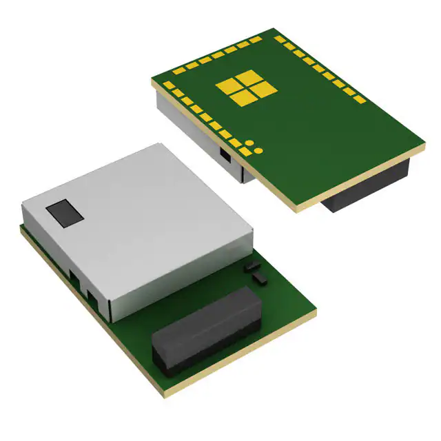
CC2650MODA
SWRS187D – AUGUST 2016 – REVISED JULY 2019
CC2650MODA SimpleLink™ Bluetooth® low energy Wireless MCU Module
1 Device Overview
1.1
Features
1
• Microcontroller
– Powerful ARM® Cortex®-M3
– EEMBC CoreMark® Score: 142
– Up to 48-MHz Clock Speed
– 128KB of In-System Programmable Flash
– 8KB of SRAM for Cache
– 20KB of Ultra-Low-Leakage SRAM
– 2-Pin cJTAG and JTAG Debugging
– Supports Over-The-Air (OTA) Upgrade
• Ultra-Low-Power Sensor Controller
– Can Run Autonomous From the Rest of the
System
– 16-Bit Architecture
– 2KB of Ultra-Low-Leakage SRAM for
Code and Data
• Efficient Code Size Architecture, Placing Drivers,
Bluetooth® low energy Controller, IEEE® 802.15.4
Medium Access Control (MAC), and Bootloader in
ROM
• Integrated Antenna
• Peripherals
– All Digital Peripheral Pins Can Be Routed to
Any GPIO
– Four General-Purpose Timer Modules
(8 × 16-Bit or 4 × 32-Bit Timer, PWM Each)
– 12-Bit ADC, 200-ksamples/s, 8-Channel
Analog MUX
– Continuous Time Comparator
– Ultra-Low-Power Analog Comparator
– Programmable Current Source
– UART
– 2 × SSI (SPI, MICROWIRE, TI)
– I2C
– I2S
– Real-Time Clock (RTC)
– AES-128 Security Module
– True Random Number Generator (TRNG)
– 15 GPIOs
– Support for Eight Capacitive Sensing Buttons
– Integrated Temperature Sensor
• External System
– On-Chip Internal DC-DC Converter
– No External Components Needed, Only Supply
Voltage
• Low Power
– Wide Supply Voltage Range
– Operation from 1.8 to 3.8 V
– Active-Mode RX: 6.2 mA
– Active-Mode TX at 0 dBm: 6.8 mA
– Active-Mode TX at +5 dBm: 9.4 mA
– Active-Mode MCU: 61 µA/MHz
– Active-Mode MCU: 48.5 CoreMark/mA
– Active-Mode Sensor Controller:
0.4 mA + 8.2 µA/MHz
– Standby: 1 µA (RTC Running and RAM/CPU
Retention)
– Shutdown: 100 nA (Wake Up on External
Events)
• RF Section
– 2.4-GHz RF Transceiver Compatible With
Bluetooth low energy (BLE) 5.1 Specification
and IEEE 802.15.4 PHY and MAC
– CC2650MODA RF-PHY Qualified (QDID:
88415)
– Excellent Receiver Sensitivity (–97 dBm for
Bluetooth low energy and –100 dBm for
802.15.4), Selectivity, and Blocking
Performance
– Programmable Output Power up to +5 dBm
– Pre-certified for Compliance With Worldwide
Radio Frequency Regulations
– ETSI RED (Europe)
– IC (Canada)
– FCC (USA)
– ARIB STD-T66 (Japan)
– JATE (Japan)
• Tools and Development Environment
– Full-Feature and Low-Cost Development Kits
– Multiple Reference Designs for Different RF
Configurations
– Packet Sniffer PC Software
– Sensor Controller Studio
– SmartRF™ Studio
– SmartRF Flash Programmer 2
– IAR Embedded Workbench® for ARM
– Code Composer Studio™
1
An IMPORTANT NOTICE at the end of this data sheet addresses availability, warranty, changes, use in safety-critical applications,
intellectual property matters and other important disclaimers. PRODUCTION DATA.
�CC2650MODA
SWRS187D – AUGUST 2016 – REVISED JULY 2019
1.2
•
•
•
•
•
Applications
Building Automation
Medical and Health
Appliances
Industrial
Consumer Electronics
1.3
www.ti.com
•
•
•
•
Proximity Tags
Alarm and Security
Remote Controls
Wireless Sensor Networks
Description
The SimpleLink™ CC2650MODA device is a wireless microcontroller (MCU) module that targets
Bluetooth® low energy applications. The CC2650MODA device can also run ZigBee® and 6LoWPAN and
ZigBee RF4CE™ remote control applications.
The module is based on the SimpleLink CC2650 wireless MCU, a member of the CC26xx family of costeffective, ultra-low-power, 2.4-GHz RF devices. Very-low active RF and MCU current and low-power mode
current consumption provide excellent battery lifetime and allow for operation on small coin-cell batteries
and in energy-harvesting applications.
The CC2650MODA module contains a 32-bit ARM Cortex-M3 processor that runs at 48 MHz as the main
processor and a rich peripheral feature set that includes a unique ultra-low-power sensor controller. This
sensor controller is good for interfacing with external sensors or for collecting analog and digital data
autonomously while the rest of the system is in sleep mode. Thus, the CC2650MODA device is good for
applications within a wide range of products including industrial, consumer electronics, and medical
devices.
The CC2650MODA module is pre-certified for operation under the regulations of the FCC, IC, ETSI, and
ARIB. These certifications save significant cost and effort for customers when integrating the module into
their products.
The Bluetooth low energy controller and the IEEE 802.15.4 MAC are embedded in the ROM and are partly
running on a separate ARM® Cortex®-M0 processor. This architecture improves overall system
performance and power consumption and makes more flash memory available.
The Bluetooth low energy software stack (BLE-Stack) and the ZigBee software stack ( Z-Stack™) are
available free of charge.
Device Information (1)
PART NUMBER
CC2650MODAMOH
(1)
2
PACKAGE
BODY SIZE
MOH (Module)
16.90 mm × 11.00 mm
For more information, see Section 10.
Device Overview
Copyright © 2016–2019, Texas Instruments Incorporated
Submit Documentation Feedback
Product Folder Links: CC2650MODA
�CC2650MODA
www.ti.com
1.4
SWRS187D – AUGUST 2016 – REVISED JULY 2019
Functional Block Diagram
Figure 1-1 is a block diagram for the CC2650MODA device.
SimpleLink CC2650MODA Wireless MCU Module
32.768-kHz
Crystal
Oscillator
24-MHz Crystal
Oscillator
RF Balun
cJTAG
RF core
ROM
Main CPU
ADC
ADC
128-KB
Flash
ARM
Cortex-M3
Digital PLL
DSP Modem
8-KB
Cache
20-KB
SRAM
ROM
Sensor Controller
General Peripherals / Modules
I2C
4× 32-bit Timers
UART
2× SSI (SPI, µWire, TI)
4-KB
SRAM
ARM
Cortex-M0
Sensor Controller Engine
12-bit ADC, 200 ks/s
I2S
Watchdog Timer
2× Analog Comparators
15 GPIOs
TRNG
SPI / I2C Digital Sensor IF
AES
Temp. / Batt. Monitor
Constant Current Source
32 ch. µDMA
RTC
Time-to-Digital Converter
2-KB SRAM
DC-DC Converter
Copyright © 2017, Texas Instruments Incorporated
Figure 1-1. CC2650MODA Block Diagram
Device Overview
Copyright © 2016–2019, Texas Instruments Incorporated
Submit Documentation Feedback
Product Folder Links: CC2650MODA
3
�CC2650MODA
SWRS187D – AUGUST 2016 – REVISED JULY 2019
www.ti.com
Table of Contents
Device Overview ......................................... 1
6.2
Functional Block Diagram ........................... 24
1.1
Features .............................................. 1
6.3
Main CPU ........................................... 25
1.2
Applications ........................................... 2
6.4
RF Core ............................................. 25
1.3
Description ............................................ 2
6.5
Sensor Controller
1.4
Functional Block Diagram ............................ 3
6.6
Memory .............................................. 27
2
3
Revision History ......................................... 5
Device Comparison ..................................... 6
6.7
Debug
6.8
Power Management ................................. 28
4
Terminal Configuration and Functions .............. 7
1
Related Products ..................................... 6
3.1
5
4.1
Module Pin Diagram .................................. 7
4.2
Pin Functions ......................................... 8
............................................ 9
Absolute Maximum Ratings .......................... 9
ESD Ratings .......................................... 9
Recommended Operating Conditions ................ 9
Power Consumption Summary...................... 10
General Characteristics ............................. 10
Antenna ............................................. 11
1-Mbps GFSK (Bluetooth low energy) – RX ........ 11
1-Mbps GFSK (Bluetooth low energy) – TX ........ 12
Specifications
5.1
5.2
5.3
5.4
5.5
5.6
5.7
5.8
5.9
5.10
5.11
5.12
5.13
5.14
5.15
5.16
5.17
5.18
5.19
5.20
5.21
5.22
6
4
8
IEEE 802.15.4 (Offset Q-PSK DSSS, 250 kbps) –
RX ................................................... 12
IEEE 802.15.4 (Offset Q-PSK DSSS, 250 kbps) –
TX ................................................... 13
.............
32.768-kHz Crystal Oscillator (XOSC_LF) ..........
48-MHz RC Oscillator (RCOSC_HF) ...............
32-kHz RC Oscillator (RCOSC_LF).................
ADC Characteristics.................................
Temperature Sensor ................................
Battery Monitor ......................................
Continuous Time Comparator .......................
Low-Power Clocked Comparator ...................
Programmable Current Source .....................
DC Characteristics ..................................
24-MHz Crystal Oscillator (XOSC_HF)
13
13
13
13
14
15
15
15
15
16
16
Thermal Resistance Characteristics for MOH
Package ............................................. 17
...............................
5.24 Switching Characteristics ...........................
5.25 Typical Characteristics ..............................
Detailed Description ...................................
6.1
Overview ............................................
5.23
7
Timing Requirements
17
17
20
24
24
9
...................................
...............................................
......................................
..................
6.11 System Architecture .................................
6.12 Certification ..........................................
6.13 End Product Labeling ...............................
6.14 Manual Information to the End User ................
6.15 Module Marking .....................................
Application, Implementation, and Layout .........
7.1
Application Information ..............................
7.2
Layout ...............................................
26
27
6.9
Clock Systems
29
6.10
General Peripherals and Modules
29
30
30
32
32
33
34
34
35
Environmental Requirements and
Specifications ........................................... 36
8.1
PCB Bending ........................................ 36
8.2
Handling Environment
8.3
Storage Condition ................................... 36
8.4
Baking Conditions ................................... 36
8.5
Soldering and Reflow Condition
..............................
....................
36
37
Device and Documentation Support ............... 38
9.1
Device Nomenclature ............................... 38
9.2
Tools and Software
9.3
Documentation Support ............................. 40
9.4
Texas Instruments Low-Power RF Website
9.5
Low-Power RF eNewsletter ......................... 40
9.6
Community Resources .............................. 41
9.7
Additional Information ............................... 41
9.8
Trademarks.......................................... 41
.................................
........
39
40
9.9
Electrostatic Discharge Caution ..................... 42
9.10
Export Control Notice
9.11
Glossary ............................................. 42
...............................
42
10 Mechanical, Packaging, and Orderable
Information .............................................. 42
..............................
..................
PACKAGE MATERIALS INFORMATION ...........
10.1
Packaging Information
42
10.2
PACKAGE OPTION ADDENDUM
43
10.3
Table of Contents
44
Copyright © 2016–2019, Texas Instruments Incorporated
Submit Documentation Feedback
Product Folder Links: CC2650MODA
�CC2650MODA
www.ti.com
SWRS187D – AUGUST 2016 – REVISED JULY 2019
2 Revision History
NOTE: Page numbers for previous revisions may differ from page numbers in the current version.
Changes from July 1, 2017 to July 31, 2019
•
•
Page
Added Module Marking section. .................................................................................................. 33
Added Environmental Requirements and Specifications section. ............................................................ 36
Revision History
Copyright © 2016–2019, Texas Instruments Incorporated
Submit Documentation Feedback
Product Folder Links: CC2650MODA
5
�CC2650MODA
SWRS187D – AUGUST 2016 – REVISED JULY 2019
www.ti.com
3 Device Comparison
Table 3-1. Device Family Overview
DEVICE
CC2650MODAMOH
(1)
3.1
PHY SUPPORT
Multiprotocol
(1)
FLASH (KB)
RAM (KB)
GPIO
PACKAGE
128
20
15
MOH
The CC2650 device supports all PHYs and can be reflashed to run all the supported standards.
Related Products
TI's Wireless Connectivity The wireless connectivity portfolio offers a wide selection of low-power RF
solutions suitable for a broad range of applications. The offerings range from fully
customized solutions to turn key offerings with pre-certified hardware and software
(protocol).
TI's SimpleLink™ Sub-1 GHz Wireless MCUs Long-range, low-power wireless connectivity solutions
are offered in a wide range of Sub-1 GHz ISM bands.
Companion Products Review products that are frequently purchased or used in conjunction with this
product.
SimpleLink™ CC2650 Wireless MCU LaunchPad™ Development Kit
The CC2650 LaunchPad™
development kit brings easy Bluetooth® low energy connectivity to the LaunchPad kit
ecosystem with the SimpleLink ultra-low power CC26xx family of devices. This LaunchPad
kit also supports development for multi-protocol support for the SimpleLink multi-standard
CC2650 wireless MCU and the rest of CC26xx family of products: CC2630 wireless MCU for
ZigBee®/6LoWPAN and CC2640 wireless MCU for Bluetooth low energy.
Reference Designs for CC2650MODA TI Designs Reference Design Library is a robust reference design
library spanning analog, embedded processor and connectivity. Created by TI experts to
help you jump-start your system design, all TI Designs include schematic or block diagrams,
BOMs, and design files to speed your time to market. Search and download designs at
ti.com/tidesigns.
6
Device Comparison
Copyright © 2016–2019, Texas Instruments Incorporated
Submit Documentation Feedback
Product Folder Links: CC2650MODA
�CC2650MODA
www.ti.com
SWRS187D – AUGUST 2016 – REVISED JULY 2019
4 Terminal Configuration and Functions
Section 4.1 shows pin assignments for the CC2650MODA device.
4.1
Module Pin Diagram
Antenna
GND
1
25 GND
NC
2
24 NC
GND
3
23 VDD
DIO 0
4
22 VDD
DIO 1
5
DIO 2
6
DIO 3
7
DIO 4
8
21 DIO 14
G1
G2
G3
G4
20 DIO 13
19 DIO 12
18 DIO 11
(Exposed GND Pads)
17 DIO 10
JTAG_TMS 9
13
14
15
16
nRESET
DIO 7
DIO 8
DIO 9
(2)
12
DIO 5/JTAG_TDO
JTAG_TCK
(1)
11
DIO 6/JTAG_TDI
10
The following I/O pins marked in bold in the pinout have high-drive capabilities:
•
DIO 2
•
DIO 3
•
DIO 4
•
JTAG_TMS
•
DIO 5/JTAG_TDO
•
DIO 6/JTAG_TDI
The following I/O pins marked in italics in the pinout have analog capabilities:
•
DIO 7
•
DIO 8
•
DIO 9
•
DIO 10
•
DIO 11
•
DIO 12
•
DIO 13
•
DIO 14
Figure 4-1. CC2650MODA MOH Package
(16.9-mm × 11-mm) Module Pinout
Terminal Configuration and Functions
Copyright © 2016–2019, Texas Instruments Incorporated
Submit Documentation Feedback
Product Folder Links: CC2650MODA
7
�CC2650MODA
SWRS187D – AUGUST 2016 – REVISED JULY 2019
4.2
www.ti.com
Pin Functions
Table 4-1 describes the CC2650MODA pins.
Table 4-1. Signal Descriptions – MOH Package
PIN NAME
PIN NO.
PIN TYPE
DESCRIPTION
DIO_0
4
Digital I/O
GPIO, Sensor Controller
DIO_1
5
Digital I/O
GPIO, Sensor Controller
DIO_2
6
Digital I/O
GPIO, Sensor Controller, high-drive capability
DIO_3
7
Digital I/O
GPIO, Sensor Controller, high-drive capability
DIO_4
8
Digital I/O
GPIO, Sensor Controller, high-drive capability
DIO_5/JTAG_TDO
11
Digital I/O
GPIO, high-drive capability, JTAG_TDO
DIO_6/JTAG_TDI
12
Digital I/O
GPIO, high-drive capability, JTAG_TDI
DIO_7
14
Digital I/O, Analog I/O
GPIO, Sensor Controller, analog
DIO_8
15
Digital I/O, Analog I/O
GPIO, Sensor Controller, analog
DIO_9
16
Digital I/O, Analog I/O
GPIO, Sensor Controller, analog
DIO_10
17
Digital I/O, Analog I/O
GPIO, Sensor Controller, analog
DIO_11
18
Digital I/O, Analog I/O
GPIO, Sensor Controller, analog
DIO_12
19
Digital I/O, Analog I/O
GPIO, Sensor Controller, analog
DIO_13
20
Digital I/O, Analog I/O
GPIO, Sensor Controller, analog
DIO_14
21
Digital I/O, Analog I/O
GPIO, Sensor Controller, analog
EGP
G1, G2, G3, G4
Power
Ground – Exposed ground pad
GND
1, 3, 25
—
Ground
JTAG_TCK
10
Digital I/O
JTAG TCKC
JTAG_TMS
9
Digital I/O
JTAG TMSC, high-drive capability
NC
2, 24
NC
Not Connected—TI recommends leaving these pins floating
nRESET
13
Digital input
Reset, active low. No internal pullup
VDD
22, 23
Power
1.8-V to 3.8-V main chip supply
8
Terminal Configuration and Functions
Copyright © 2016–2019, Texas Instruments Incorporated
Submit Documentation Feedback
Product Folder Links: CC2650MODA
�CC2650MODA
www.ti.com
SWRS187D – AUGUST 2016 – REVISED JULY 2019
5 Specifications
5.1
Absolute Maximum Ratings
over operating free-air temperature range (unless otherwise noted) (1) (2)
VDD
Supply voltage
Voltage on any digital pin
Vin
(3)
Voltage on ADC input
MIN
MAX
UNIT
–0.3
4.1
V
V
–0.3
VDD + 0.3, max 4.1
Voltage scaling enabled
–0.3
VDD
Voltage scaling disabled, internal reference
–0.3
1.49
Voltage scaling disabled, VDD as reference
–0.3
VDD / 2.9
5
dBm
–40
85
°C
Input RF level
Tstg
(1)
(2)
(3)
Storage temperature
V
Stresses beyond those listed under Absolute Maximum Ratings may cause permanent damage to the device. These are stress ratings
only, and functional operation of the device at these or any other conditions beyond those indicated under Recommended Operating
Conditions is not implied. Exposure to absolute-maximum-rated conditions for extended periods may affect device reliability.
All voltage values are with respect to ground, unless otherwise noted.
Including analog capable DIO.
5.2
ESD Ratings
VALUE
Human body model (HBM), per ANSI/ESDA/JEDEC
JS001 (1)
VESD
Electrostatic discharge
Charged device model (CDM), per JESD22-C101 (2)
(1)
(2)
5.3
All pins
±1000
RF pins
±500
Non-RF pins
±500
UNIT
V
JEDEC document JEP155 states that 500-V HBM allows safe manufacturing with a standard ESD control process.
JEDEC document JEP157 states that 250-V CDM allows safe manufacturing with a standard ESD control process.
Recommended Operating Conditions
Ambient temperature
Operating supply voltage (VDD)
For operation in battery-powered and 3.3-V systems
(internal DC-DC can be used to minimize power
consumption)
MIN
MAX
–40
85
°C
1.8
3.8
V
Specifications
Copyright © 2016–2019, Texas Instruments Incorporated
Submit Documentation Feedback
Product Folder Links: CC2650MODA
UNIT
9
�CC2650MODA
SWRS187D – AUGUST 2016 – REVISED JULY 2019
5.4
www.ti.com
Power Consumption Summary
Tc = 25°C, VDD = 3.0 V with internal DC-DC converter, unless otherwise noted
PARAMETER
Icore
Core current
consumption
TEST CONDITIONS
MIN
TYP
Reset. RESET_N pin asserted or VDD below Power-onReset threshold
100
Shutdown. No clocks running, no retention
150
Standby. With RTC, CPU, RAM and (partial) register
retention. RCOSC_LF
1
Standby. With RTC, CPU, RAM and (partial) register
retention. XOSC_LF
1.2
Standby. With Cache, RTC, CPU, RAM and (partial)
register retention. RCOSC_LF
2.5
Standby. With Cache, RTC, CPU, RAM and (partial)
register retention. XOSC_LF
2.7
Idle. Supply systems and RAM powered.
MAX
UNIT
nA
µA
550
1.45 mA +
31 µA/MHz
Active. Core running CoreMark
Radio RX
6.2
Radio TX, 0-dBm output power
6.8
Radio TX, 5-dBm output power
9.4
mA
Peripheral Current Consumption (Adds to core current Icore for each peripheral unit activated) (1)
Iperi
(1)
5.5
Peripheral power
domain
Delta current with domain enabled
20
Serial power domain
Delta current with domain enabled
13
RF core
Delta current with power domain enabled, clock
enabled, RF Core Idle
237
µDMA
Delta current with clock enabled, module idle
130
Timers
Delta current with clock enabled, module idle
113
I2C
Delta current with clock enabled, module idle
12
I2S
Delta current with clock enabled, module idle
36
SSI
Delta current with clock enabled, module idle
93
UART
Delta current with clock enabled, module idle
164
µA
Iperi is not supported in Standby or Shutdown.
General Characteristics
Tc = 25°C, VDD = 3.0 V, unless otherwise noted
PARAMETER
TEST CONDITIONS
MIN
TYP
MAX
UNIT
FLASH MEMORY
Supported flash erase cycles before
failure
Flash page/sector erase current
100
Average delta current
Flash page/sector erase time (1)
Flash page/sector size
Flash write current
Average delta current, 4 bytes at a time
Flash write time (1)
4 bytes at a time
(1)
10
k Cycles
12.6
mA
8
ms
4
KB
8.15
mA
8
µs
This number is dependent on flash aging and will increase over time and erase cycles.
Specifications
Copyright © 2016–2019, Texas Instruments Incorporated
Submit Documentation Feedback
Product Folder Links: CC2650MODA
�CC2650MODA
www.ti.com
5.6
SWRS187D – AUGUST 2016 – REVISED JULY 2019
Antenna
Tc = 25°C, VDD = 3.0 V, unless otherwise noted.
PARAMETER
TEST CONDITIONS
MIN
Polarization
TYP
UNIT
Linear
Peak Gain
2450 MHz
1.26
Efficiency
2450 MHz
57%
5.7
MAX
dBi
1-Mbps GFSK (Bluetooth low energy) – RX
RF performance is specified in a single ended 50-Ω reference plane at the antenna feeding point with Tc = 25°C,
VDD = 3.0 V, fRF = 2440 MHz, unless otherwise noted.
PARAMETER
TEST CONDITIONS
MIN
TYP
MAX
UNIT
Receiver sensitivity
BER = 10
–3
–97
dBm
Receiver saturation
BER = 10–3
4
dBm
Frequency error tolerance
Difference between center frequency of the received RF signal
and local oscillator frequency.
Data rate error tolerance
–350
350
kHz
–750
750
ppm
Co-channel rejection (1)
Wanted signal at –67 dBm, modulated interferer in channel,
BER = 10–3
–6
dB
Selectivity, ±1 MHz (1)
Wanted signal at –67 dBm, modulated interferer at ±1 MHz,
BER = 10–3
7 / 3 (2)
dB
Selectivity, ±2 MHz (1)
Wanted signal at –67 dBm, modulated interferer at ±2 MHz,
BER = 10–3
29 / 23 (2)
dB
Selectivity, ±3 MHz (1)
Wanted signal at –67 dBm, modulated interferer at ±3 MHz,
BER = 10–3
38 / 26 (2)
dB
Selectivity, ±4 MHz (1)
Wanted signal at –67 dBm, modulated interferer at ±4 MHz,
BER = 10–3
42 / 29 (2)
dB
Selectivity, ±5 MHz or more (1)
Wanted signal at –67 dBm, modulated interferer at ≥ ±5 MHz,
BER = 10–3
32
dB
Selectivity, Image frequency (1)
Wanted signal at –67 dBm, modulated interferer at image
frequency, BER = 10–3
23
dB
Selectivity,
Image frequency ±1 MHz (1)
Wanted signal at –67 dBm, modulated interferer at ±1 MHz from
image frequency, BER = 10–3
3 / 26 (2)
dB
Out-of-band blocking (3)
30 MHz to 2000 MHz
–20
dBm
Out-of-band blocking
2003 MHz to 2399 MHz
–5
dBm
Out-of-band blocking
2484 MHz to 2997 MHz
–8
dBm
Out-of-band blocking
3000 MHz to 12.75 GHz
–8
dBm
Intermodulation
Wanted signal at 2402 MHz, –64 dBm. Two interferers at 2405
and 2408 MHz respectively, at the given power level
–34
dBm
Spurious emissions,
30 MHz to 1000 MHz
Conducted measurement in a 50-Ω single-ended load. Suitable
for systems targeting compliance with EN 300 328, EN 300 440
class 2, FCC CFR47, Part 15 and ARIB STD-T-66
–71
dBm
Spurious emissions,
1 GHz to 12.75 GHz
Conducted measurement in a 50-Ω single-ended load. Suitable
for systems targeting compliance with EN 300 328, EN 300 440
class 2, FCC CFR47, Part 15 and ARIB STD-T-66
–62
dBm
RSSI dynamic range
70
dB
RSSI accuracy
±4
dB
(1)
(2)
(3)
Numbers given as I/C dB
X / Y, where X is +N MHz and Y is –N MHz
Excluding one exception at Fwanted / 2, per Bluetooth Specification
Specifications
Copyright © 2016–2019, Texas Instruments Incorporated
Submit Documentation Feedback
Product Folder Links: CC2650MODA
11
�CC2650MODA
SWRS187D – AUGUST 2016 – REVISED JULY 2019
5.8
www.ti.com
1-Mbps GFSK (Bluetooth low energy) – TX
RF performance is specified in a single ended 50-Ω reference plane at the antenna feeding point with Tc = 25°C,
VDD = 3.0 V, fRF = 2440 MHz, unless otherwise noted.
PARAMETER
TEST CONDITIONS
MIN
Output power, highest setting
Output power, lowest setting
Spurious emission conducted
measurement (1)
(1)
5.9
TYP
MAX
UNIT
5
dBm
–21
dBm
f < 1 GHz, outside restricted bands
–43
f < 1 GHz, restricted bands ETSI
–58
f < 1 GHz, restricted bands FCC
–57
f > 1 GHz, including harmonics
–45
dBm
Suitable for systems targeting compliance with worldwide radio-frequency regulations ETSI EN 300 328 and EN 300 440 Class 2
(Europe), FCC CFR47 Part 15 (US), and ARIB STD-T66 (Japan)
IEEE 802.15.4 (Offset Q-PSK DSSS, 250 kbps) – RX
RF performance is specified in a single ended 50-Ω reference plane at the antenna feeding point with Tc = 25°C,
VDD = 3.0 V, unless otherwise noted.
PARAMETER
TEST CONDITIONS
MIN
TYP
MAX
UNIT
Receiver sensitivity
PER = 1%
–100
dBm
Receiver saturation
PER = 1%
–7
dBm
Adjacent channel rejection
Wanted signal at –82 dBm, modulated interferer at ±5 MHz,
PER = 1%
35
dB
Alternate channel rejection
Wanted signal at –82 dBm, modulated interferer at ±10 MHz,
PER = 1%
52
dB
Channel rejection, ±15 MHz or
more
Wanted signal at –82 dBm, undesired signal is IEEE 802.15.4
modulated channel, stepped through all channels 2405 to
2480 MHz, PER = 1%
57
dB
Blocking and desensitization,
5 MHz from upper band edge
Wanted signal at –97 dBm (3 dB above the sensitivity level),
CW jammer, PER = 1%
64
dB
Blocking and desensitization,
10 MHz from upper band edge
Wanted signal at –97 dBm (3 dB above the sensitivity level),
CW jammer, PER = 1%
64
dB
Blocking and desensitization,
20 MHz from upper band edge
Wanted signal at –97 dBm (3 dB above the sensitivity level),
CW jammer, PER = 1%
65
dB
Blocking and desensitization,
50 MHz from upper band edge
Wanted signal at –97 dBm (3 dB above the sensitivity level),
CW jammer, PER = 1%
68
dB
Blocking and desensitization,
–5 MHz from lower band edge
Wanted signal at –97 dBm (3 dB above the sensitivity level),
CW jammer, PER = 1%
63
dB
Blocking and desensitization,
–10 MHz from lower band edge
Wanted signal at –97 dBm (3 dB above the sensitivity level),
CW jammer, PER = 1%
63
dB
Blocking and desensitization,
–20 MHz from lower band edge
Wanted signal at –97 dBm (3 dB above the sensitivity level),
CW jammer, PER = 1%
65
dB
Blocking and desensitization,
–50 MHz from lower band edge
Wanted signal at –97 dBm (3 dB above the sensitivity level),
CW jammer, PER = 1%
67
dB
Spurious emissions,
30 MHz to 1000 MHz
Conducted measurement in a 50-Ω single-ended load.
Suitable for systems targeting compliance with EN 300 328,
EN 300 440 class 2, FCC CFR47, Part 15 and ARIB STD-T66
–71
dBm
Spurious emissions,
1 GHz to 12.75 GHz
Conducted measurement in a 50-Ω single-ended load.
Suitable for systems targeting compliance with EN 300 328,
EN 300 440 class 2, FCC CFR47, Part 15 and ARIB STD-T66
–62
dBm
Frequency error tolerance
Difference between center frequency of the received RF
signal and local oscillator frequency
>200
ppm
100
dB
±4
dB
RSSI dynamic range
RSSI accuracy
12
Specifications
Copyright © 2016–2019, Texas Instruments Incorporated
Submit Documentation Feedback
Product Folder Links: CC2650MODA
�CC2650MODA
www.ti.com
SWRS187D – AUGUST 2016 – REVISED JULY 2019
5.10 IEEE 802.15.4 (Offset Q-PSK DSSS, 250 kbps) – TX
RF performance is specified in a single ended 50-Ω reference plane at the antenna feeding point with Tc = 25°C,
VDD = 3.0 V, unless otherwise noted.
PARAMETER
TEST CONDITIONS
MIN
Output power, highest setting
Output power, lowest setting
Error vector magnitude
Spurious emission conducted
measurement (1)
(1)
TYP
MAX
UNIT
5
dBm
–21
dBm
At maximum output power
2%
f < 1 GHz, outside restricted bands
–43
f < 1 GHz, restricted bands ETSI
–58
f < 1 GHz, restricted bands FCC
–57
f > 1 GHz, including harmonics
–45
dBm
Suitable for systems targeting compliance with worldwide radio-frequency regulations ETSI EN 300 328 and EN 300 440 Class 2
(Europe), FCC CFR47 Part 15 (US), and ARIB STD-T66 (Japan)
5.11 24-MHz Crystal Oscillator (XOSC_HF) (1)
over operating free-air temperature range (unless otherwise noted)
PARAMETER
TEST CONDITIONS
MIN
Crystal frequency
Start-up time
(3)
MAX
24
Crystal frequency tolerance (2)
(1)
(2)
TYP
–40
(3)
UNIT
MHz
40
ppm
150
µs
Probing or otherwise stopping the XTAL while the DC-DC converter is enabled may cause permanent damage to the device.
Includes initial tolerance of the crystal, drift over temperature, aging and frequency pulling due to incorrect load capacitance. As per
Bluetooth and IEEE 802.15.4 specification
Kick-started based on a temperature and aging compensated RCOSC_HF using precharge injection
5.12 32.768-kHz Crystal Oscillator (XOSC_LF)
over operating free-air temperature range (unless otherwise noted)
PARAMETER
TEST CONDITIONS
MIN
Crystal frequency
Initial crystal frequency tolerance, Bluetooth
low energy applications
TYP
MAX
32.768
Tc = 25°C
Crystal aging
UNIT
kHz
–20
20
ppm
-3
3
ppm/year
5.13 48-MHz RC Oscillator (RCOSC_HF)
Tc = 25°C, VDD = 3.0 V, unless otherwise noted
PARAMETER
TEST CONDITIONS
MIN
Frequency
TYP
48
Uncalibrated frequency accuracy
±1%
Calibrated frequency accuracy (1)
±0.25%
Start-up time
(1)
MAX
UNIT
MHz
5
µs
Accuracy relatively to the calibration source (XOSC_HF).
5.14 32-kHz RC Oscillator (RCOSC_LF)
Tc = 25°C, VDD = 3.0 V, unless otherwise noted
PARAMETER
TEST CONDITIONS
Calibrated frequency
MIN
TYP
32.8
Temperature coefficient
50
MAX
UNIT
kHz
ppm/°C
Specifications
Copyright © 2016–2019, Texas Instruments Incorporated
Submit Documentation Feedback
Product Folder Links: CC2650MODA
13
�CC2650MODA
SWRS187D – AUGUST 2016 – REVISED JULY 2019
www.ti.com
5.15 ADC Characteristics
Tc = 25°C, VDD = 3.0 V and voltage scaling enabled, unless otherwise noted
PARAMETER
(1)
TEST CONDITIONS
MIN
Input voltage range
TYP
0
VDD
Resolution
12
Sample rate
Offset
Gain error
DNL (3)
Differential nonlinearity
INL (4)
Integral nonlinearity
Internal 4.3-V equivalent reference
(2)
, 200 ksps,
THD
(1)
(2)
(3)
(4)
(5)
14
LSB
2.4
LSB
>–1
LSB
±3
LSB
10
Bits
11.1
(2)
, 200 ksps,
–65
VDD as reference, 200 ksps, 9.6-kHz input tone
–69
Internal 1.44-V reference, voltage scaling disabled,
32 samples average, 200 ksps, 300-Hz input tone
–71
dB
Internal 4.3-V equivalent reference (2), 200 ksps,
9.6-kHz input tone
60
VDD as reference, 200 ksps, 9.6-kHz input tone
63
Internal 1.44-V reference, voltage scaling disabled,
32 samples average, 200 ksps, 300-Hz input tone
69
Internal 4.3-V equivalent reference (2), 200 ksps,
9.6-kHz input tone
67
VDD as reference, 200 ksps, 9.6-kHz input tone
72
Internal 1.44-V reference, voltage scaling disabled, 32
samples average, 200 ksps, 300-Hz input tone
73
Conversion time
Serial conversion, time-to-output, 24-MHz clock
50
Current consumption
Internal 4.3-V equivalent reference (2)
0.66
mA
Current consumption
VDD as reference
0.75
mA
Reference voltage
Equivalent fixed internal reference (input voltage
scaling enabled). For best accuracy, the ADC
conversion should be initiated through the TI-RTOS™
API to include the gain or offset compensation factors
stored in FCFG1.
SINAD
Signal-to-noise and
and SNDR distortion ratio
SFDR
ksps
2
9.8
Internal 1.44-V reference, voltage scaling disabled,
32 samples average, 200 ksps, 300-Hz input tone
Total harmonic
distortion
V
(2)
Effective number of bits VDD as reference, 200 ksps, 9.6-kHz input tone
Internal 4.3-V equivalent reference
9.6-kHz input tone
UNIT
Bits
200
Internal 4.3-V equivalent reference (2)
Internal 4.3-V equivalent reference
9.6-kHz input tone
ENOB
MAX
Spurious-free dynamic
range
dB
dB
clockcycles
4.3 (2) (5)
V
Reference voltage
Fixed internal reference (input voltage scaling
disabled). For best accuracy, the ADC conversion
should be initiated through the TI-RTOS API to include
the gain or offset compensation factors stored in
FCFG1. This value is derived from the scaled value
(4.3 V) as follows: Vref = 4.3 V × 1408 / 4095
1.48
V
Reference voltage
VDD as reference (Also known as RELATIVE) (input
voltage scaling enabled)
VDD
V
Reference voltage
VDD as reference (Also known as RELATIVE) (input
voltage scaling disabled)
VDD / 2.82 (5)
V
Input Impedance
200 ksps, voltage scaling enabled. Capacitive input,
input impedance depends on sampling frequency and
sampling time
>1
MΩ
Using IEEE Std 1241™-2010 for terminology and test methods.
Input signal scaled down internally before conversion, as if voltage range was 0 to 4.3 V.
No missing codes. Positive DNL typically varies from +0.3 to +3.5 depending on device, see Figure 5-24.
For a typical example, see Figure 5-25.
Applied voltage must be within absolute maximum ratings (see Section 5.1) at all times.
Specifications
Copyright © 2016–2019, Texas Instruments Incorporated
Submit Documentation Feedback
Product Folder Links: CC2650MODA
�CC2650MODA
www.ti.com
SWRS187D – AUGUST 2016 – REVISED JULY 2019
5.16 Temperature Sensor
Tc = 25°C, VDD = 3.0 V, unless otherwise noted
PARAMETER
TEST CONDITIONS
MIN
Resolution
TYP
MAX
4
Range
–40
UNIT
°C
85
°C
Accuracy
±5
°C
Supply voltage coefficient (1)
3.2
°C/V
(1)
Automatically compensated when using supplied driver libraries.
5.17 Battery Monitor
Tc = 25°C, VDD = 3.0 V, unless otherwise noted
PARAMETER
TEST CONDITIONS
MIN
Resolution
TYP
MAX
50
Range
1.8
Accuracy
UNIT
mV
3.8
13
V
mV
5.18 Continuous Time Comparator
Tc = 25°C, VDD = 3.0 V, unless otherwise noted
PARAMETER
TEST CONDITIONS
MIN
TYP
MAX
UNIT
Input voltage range
0
VDD
V
External reference voltage
0
VDD
V
Internal reference voltage
DCOUPL as reference
1.27
Offset
Hysteresis
Decision time
Step from –10 mV to +10 mV
Current consumption when enabled (1)
(1)
V
3
mV