SN74CB3Q3306A-EP
www.ti.com
SCDS352 – DECEMBER 2013
Dual FET Bus Switch 2.5-V/3.3-V Low-Voltage High-Bandwidth Bus Switch
Check for Samples: SN74CB3Q3306A-EP
FEATURES
1
High-Bandwidth Data Path (up to 500 MHz(1))
5-V-Tolerant I/Os With Device Powered Up or
Powered Down
Low and Flat ON-State Resistance (ron)
Characteristics Over Operating Range
(ron = 4 Ω Typ)
Rail-to-Rail Switching on Data I/O Ports
– 0- to 5-V Switching With 3.3-V VCC
– 0- to 3.3-V Switching With 2.5-V VCC
Bidirectional Data Flow With Near-Zero
Propagation Delay
Low Input/Output Capacitance Minimizes
Loading and Signal Distortion
(Cio(OFF) = 3.5 pF Typ)
Fast Switching Frequency (f OE = 20 MHz Max)
Data and Control Inputs Provide Undershoot
Clamp Diodes
Low Power Consumption (ICC = 0.25 mA Typ)
VCC Operating Range From 2.3 V to 3.6 V
Data I/Os Support 0- to 5-V Signaling Levels
(0.8 V, 1.2 V, 1.5 V, 1.8 V, 2.5 V, 3.3 V, 5 V)
Control Inputs Can Be Driven by TTL or
5-V/3.3-V CMOS Outputs
Ioff Supports Partial-Power-Down Mode
Operation
•
•
•
•
•
•
•
•
•
•
•
•
•
(1)
•
•
•
Latch-Up Performance Exceeds 100 mA
Per JESD 78, Class II
ESD Performance Tested Per JESD 22
– 2000-V Human-Body Model
(A114-B, Class II)
– 1000-V Charged-Device Model (C101)
Supports Both Digital and Analog
Applications: USB Interface, Differential Signal
Interface, Bus Isolation, Low-Distortion Signal
Gating
SUPPORTS DEFENSE, AEROSPACE,
AND MEDICAL APPLICATIONS
•
•
•
•
•
•
•
Controlled Baseline
One Assembly and Test Site
One Fabrication Site
Available in Military (–55°C to 125°C)
Temperature Range
Extended Product Life Cycle
Extended Product-Change Notification
Product Traceability
For additional information regarding the performance
characteristics of the CB3Q family, refer to the TI application
report, CBT-C, CB3T, and CB3Q Signal-Switch Families,
literature number SCDA008.
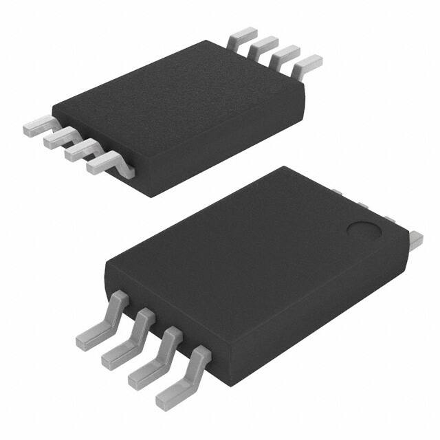
PW PACKAGE
(TOP VIEW)
1OE
1A
1B
GND
1
8
2
7
3
6
4
5
VCC
2OE
2B
2A
ORDERING INFORMATION
TJ
–55°C to 125°C
(1)
PACKAGE (1)
TSSOP – PW
Tube
Tape and reel
ORDERABLE PART
NUMBER
CCB3Q3306AMPWEP
CCB3Q3306AMPWREP
TOP-SIDE MARKING
U306AM
VID NUMBER
V62/14606-01XE-T
V62/14606-01XE
Package drawings, standard packing quantities, thermal data, symbolization, and PCB design guidelines are available at
www.ti.com/sc/package.
1
Please be aware that an important notice concerning availability, standard warranty, and use in critical applications of
Texas Instruments semiconductor products and disclaimers thereto appears at the end of this data sheet.
PRODUCTION DATA information is current as of publication date.
Products conform to specifications per the terms of the Texas
Instruments standard warranty. Production processing does not
necessarily include testing of all parameters.
Copyright © 2013, Texas Instruments Incorporated
�SN74CB3Q3306A-EP
SCDS352 – DECEMBER 2013
www.ti.com
These devices have limited built-in ESD protection. The leads should be shorted together or the device placed in conductive foam
during storage or handling to prevent electrostatic damage to the MOS gates.
DESCRIPTION
The SN74CB3Q3306A is a high-bandwidth FET bus switch utilizing a charge pump to elevate the gate voltage of
the pass transistor, providing a low and flat ON-state resistance (ron). The low and flat ON-state resistance allows
for minimal propagation delay and supports rail-to-rail switching on the data input/output (I/O) ports. The device
also features low data I/O capacitance to minimize capacitive loading and signal distortion on the data bus.
Specifically designed to support high-bandwidth applications, the SN74CB3Q3306A provides an optimized
interface solution ideally suited for broadband communications, networking, and data-intensive computing
systems.
The SN74CB3Q3306A is organized as two 1-bit switches with separate output-enable (1OE, 2OE) inputs. It can
be used as two 1-bit bus switches or as one 2-bit bus switch. When OE is low, the associated 1-bit bus switch is
ON and the A port is connected to the B port, allowing bidirectional data flow between ports. When OE is high,
the associated 1-bit bus switch is OFF, and a high-impedance state exists between the A and B ports.
This device is fully specified for partial-power-down applications using Ioff. The Ioff circuitry prevents damaging
current backflow through the device when it is powered down. The device has isolation during power off.
To ensure the high-impedance state during power up or power down, OE should be tied to VCC through a pullup
resistor; the minimum value of the resistor is determined by the current-sinking capability of the driver.
Table 1. FUNCTION TABLE
(EACH BUS SWITCH)
INPUT
OE
INPUT/OUTPUT
A
FUNCTION
L
B
A port = B port
H
Z
Disconnect
LOGIC DIAGRAM (POSITIVE LOGIC)
2
1A
1OE
3
1B
SW
1
5
2A
6
SW
2B
7
2OE
2
Submit Documentation Feedback
Copyright © 2013, Texas Instruments Incorporated
Product Folder Links :SN74CB3Q3306A-EP
�SN74CB3Q3306A-EP
www.ti.com
SCDS352 – DECEMBER 2013
Figure 1. SIMPLIFIED SCHEMATIC, EACH FET SWITCH (SW)
B
A
VCC
Charge
Pump
EN(1)
(1) EN is the internal enable signal applied to the switch.
ABSOLUTE MAXIMUM RATINGS (1)
over operating junction temperature range (unless otherwise noted)
VCC
Supply voltage range
MIN
MAX
–0.5
4.6
UNIT
V
–0.5
7
V
–0.5
7
VIN
Control input voltage range
(2) (3)
VI/O
Switch I/O voltage range (2)
(3) (4)
IIK
Control input clamp current
VIN < 0
–50
mA
II/OK
I/O port clamp current
VI/O < 0
–50
mA
II/O
ON-state switch current (5)
±64
mA
±100
mA
150
°C
150
°C
Continuous current through each VCC or
GND
TJ
Maximum junction temperature
Tstg
Storage temperature range
(1)
(2)
(3)
(4)
(5)
–65
V
Stresses beyond those listed under "absolute maximum ratings" may cause permanent damage to the device. These are stress ratings
only, and functional operation of the device at these or any other conditions beyond those indicated under "recommended operating
conditions" is not implied. Exposure to absolute-maximum-rated conditions for extended periods may affect device reliability.
All voltages are with respect to ground, unless otherwise specified.
The input and output voltage ratings may be exceeded if the input and output clamp-current ratings are observed.
VI and VO are used to denote specific conditions for VI/O.
II and IO are used to denote specific conditions for II/O.
Submit Documentation Feedback
Copyright © 2013, Texas Instruments Incorporated
Product Folder Links :SN74CB3Q3306A-EP
3
�SN74CB3Q3306A-EP
SCDS352 – DECEMBER 2013
www.ti.com
THERMAL INFORMATION
SN74CB3Q3306A-EP
THERMAL METRIC (1)
PW
UNITS
8 PINS
Junction-to-ambient thermal resistance (2)
θJA
(3)
190.6
θJCtop
Junction-to-case (top) thermal resistance
θJB
Junction-to-board thermal resistance (4)
ψJT
Junction-to-top characterization parameter (5)
ψJB
Junction-to-board characterization parameter (6)
117.7
θJCbot
Junction-to-case (bottom) thermal resistance (7)
N/A
(1)
(2)
(3)
(4)
(5)
(6)
(7)
74
119.4
°C/W
12
For more information about traditional and new thermal metrics, see the IC Package Thermal Metrics application report, SPRA953.
The junction-to-ambient thermal resistance under natural convection is obtained in a simulation on a JEDEC-standard, high-K board, as
specified in JESD51-7, in an environment described in JESD51-2a.
The junction-to-case (top) thermal resistance is obtained by simulating a cold plate test on the package top. No specific JEDECstandard test exists, but a close description can be found in the ANSI SEMI standard G30-88.
The junction-to-board thermal resistance is obtained by simulating in an environment with a ring cold plate fixture to control the PCB
temperature, as described in JESD51-8.
The junction-to-top characterization parameter, ψJT, estimates the junction temperature of a device in a real system and is extracted
from the simulation data for obtaining θJA, using a procedure described in JESD51-2a (sections 6 and 7).
The junction-to-board characterization parameter, ψJB, estimates the junction temperature of a device in a real system and is extracted
from the simulation data for obtaining θJA , using a procedure described in JESD51-2a (sections 6 and 7).
The junction-to-case (bottom) thermal resistance is obtained by simulating a cold plate test on the exposed (power) pad. No specific
JEDEC standard test exists, but a close description can be found in the ANSI SEMI standard G30-88.
Spacer
RECOMMENDED OPERATING CONDITIONS (1)
MIN MAX
VCC
Supply voltage
2.3
3.6
1.7
5.5
UNIT
V
VIH
High-level control input
voltage
VCC = 2.3 V to 2.7 V
VCC = 2.7 V to 3.6 V
2
5.5
VIL
Low-level control input
voltage
VCC = 2.3 V to 2.7 V
0
0.7
VCC = 2.7 V to 3.6 V
0
0.8
VI/O
Data input/output voltage
0
5.5
V
TJ
Operating junction temperature
–55
125
°C
(1)
4
V
V
All unused control inputs of the device must be held at VCC or GND to ensure proper device operation. Refer to the TI application report,
Implications of Slow or Floating CMOS Inputs, literature number SCBA004.
Submit Documentation Feedback
Copyright © 2013, Texas Instruments Incorporated
Product Folder Links :SN74CB3Q3306A-EP
�SN74CB3Q3306A-EP
www.ti.com
SCDS352 – DECEMBER 2013
ELECTRICAL CHARACTERISTICS (1)
over recommended operating junction temperature range (unless otherwise noted)
PARAMETER
VIK
Control
inputs
IIN
IOZ
(3)
Ioff
ICC
ΔICC
(4)
ICCD
(5)
Control
inputs
Per control
input
Control
inputs
Cin
TEST CONDITIONS
MIN
VCC = 3.6 V,
II = –18 mA
VCC = 3.6 V,
VIN = 0 to 5.5 V
VCC = 3.6 V,
VO = 0 to 5.5 V,
VI = 0,
Switch OFF,
VIN = VCC
VCC = 0,
VO = 0 to 5.5 V,
VI = 0
VCC = 3.6 V,
II/O = 0,
Switch ON or OFF,
VIN = VCC or GND
VCC = 3.6 V,
One input at 3 V,
Other inputs at VCC or GND
VCC = 3.6 V,
A and B ports open,
TYP (2)
MAX
UNIT
–1.8
V
±1
μA
±1
μA
1
μA
0.7
mA
0.25
TJ = -55°C to 85°C
25
TJ = 125°C
36
Control input switching at 50% duty cycle
μA
0.03
mA/
MHz
VCC = 3.3 V,
VIN = 5.5 V, 3.3 V, or 0
2.5
pF
Cio(OFF)
VCC = 3.3 V,
Switch OFF,
VIN = VCC,
VI/O = 5.5 V, 3.3 V, or 0
3.5
pF
Cio(ON)
VCC = 3.3 V,
Switch ON,
VIN = GND,
VI/O = 5.5 V, 3.3 V, or 0
8
pF
VI = 0,
IO = 30 mA
VI = 1.7 V,
IO = –15 mA
VI = 0,
IO = 30 mA
TJ = -55°C to 85°C
ron
(1)
(2)
(3)
(4)
(5)
(6)
5
TJ = 125°C
4
TJ = 125°C
6
Ω
8
TJ = -55°C to 85°C
IO = –15 mA
9
58
TJ = -55°C to 85°C
VCC = 3 V
8
10
TJ = -55°C to 85°C
(6)
VI = 2.4 V,
4
TJ = 125°C
VCC = 2.3 V,
TYP at VCC = 2.5 V
5
TJ = 125°C
8
66
VIN and IIN refer to control inputs. VI, VO, II, and IO refer to data pins.
All typical values are at VCC = 3.3 V (unless otherwise noted), TA = 25°C.
For I/O ports, the parameter IOZ includes the input leakage current.
This is the increase in supply current for each input that is at the specified TTL voltage level, rather than VCC or GND.
This parameter specifies the dynamic power-supply current associated with the operating frequency of a single control input (see
Figure 4).
Measured by the voltage drop between the A and B terminals at the indicated current through the switch. ON-state resistance is
determined by the lower of the voltages of the two (A or B) terminals.
100,000,000
Estimated Life (Hours)
10,000,000
WB Failure Mode
1,000,000
100,000
EM Failure Mode
10,000
1,000
80
90
100
110
120
130
140
150
Continuous Junction Temperature, TJ (°C)
(1)
See datasheet for absolute maximum and minimum recommended operating conditions.
(2)
Silicon operating life design goal is 10 years at 105°C junction temperature (does not include package interconnect
life).
(3)
Enhanced plastic product disclaimer applies.
Figure 2. SN74CB3Q3306A-EP Operating Life Derating Chart
Submit Documentation Feedback
Copyright © 2013, Texas Instruments Incorporated
Product Folder Links :SN74CB3Q3306A-EP
5
�SN74CB3Q3306A-EP
SCDS352 – DECEMBER 2013
www.ti.com
SWITCHING CHARACTERISTICS
over recommended operating junction temperature range (unless otherwise noted) (see Figure 5)
PARAMETER
f OE
tpd
(1)
TJ = -55° to 85°C
(2)
FROM
(INPUT)
TO
(OUTPUT)
OE
A or B
VCC = 2.5 V
± 0.2 V
MIN
VCC = 3.3 V
± 0.3 V
MAX
MIN
UNIT
MAX
10
20
0.2
0.3
1.2
2.3
MHz
A or B
B or A
ten
OE
A or B
1.5
12
1.5
10
ns
tdis
OE
A or B
1
14
1
9
ns
(1)
(2)
TJ = 125°C
ns
Maximum switching frequency for control input (VO > VCC, VI = 5 V, RL ≥ 1 MΩ, CL = 0)
The propagation delay is the calculated RC time constant of the typical ON-state resistance of the switch and the specified load
capacitance, when driven by an ideal voltage source (zero output impedance).
TYPICAL ron vs VI
ron − ON-State Resistance − Ω
16
VCC = 3.3 V
TA = 25°C
IO = −15 mA
14
12
10
8
6
4
2
0
0.0
0.5
1.0
1.5
2.0
2.5
3.0
3.5
4.0
4.5
5.0
18
20
VI − V
Figure 3. Typical ron vs VI
12
VCC = 3.3 V
TA = 25°C
A and B Ports Open
I CC − mA
10
8
6
4
2
One OE Switching
0
0
2
4
6
8
10
12
14
16
OE Switching Frequency − MHz
Figure 4. Typical ICC vs OE Switching Frequency
6
Submit Documentation Feedback
Copyright © 2013, Texas Instruments Incorporated
Product Folder Links :SN74CB3Q3306A-EP
�SN74CB3Q3306A-EP
www.ti.com
SCDS352 – DECEMBER 2013
PARAMETER MEASUREMENT INFORMATION
VCC
Input Generator
VIN
50 Ω
50 Ω
VG1
TEST CIRCUIT
DUT
2 × VCC
Input Generator
VI
S1
RL
VO
50 Ω
50 Ω
VG2
RL
CL
(see Note A)
TEST
VCC
S1
RL
VI
CL
tpd(s)
2.5 V ± 0.2 V
3.3 V ± 0.3 V
Open
Open
500 Ω
500 Ω
VCC or GND
VCC or GND
30 pF
50 pF
tPLZ/tPZL
2.5 V ± 0.2 V
3.3 V ± 0.3 V
2 × VCC
2 × VCC
500 Ω
500 Ω
GND
GND
30 pF
50 pF
0.15 V
0.3 V
tPHZ/tPZH
2.5 V ± 0.2 V
3.3 V ± 0.3 V
GND
GND
500 Ω
500 Ω
VCC
VCC
30 pF
50 pF
0.15 V
0.3 V
V∆
VCC
Output
Control
(VIN)
VCC/2
VCC
VCC/2
VCC/2
0V
tPLH
VOH
Output
VCC/2
tPLZ
Output
Waveform 1
S1 at 2 × VCC
(see Note B)
VCC
VCC/2
VCC/2
VOL
VOL + V∆
VOL
tPZH
tPHL
VCC/2
0V
tPZL
Output
Control
(VIN)
Open
GND
tPHZ
Output
Waveform 2
S1 at GND
(see Note B)
VOLTAGE WAVEFORMS
PROPAGATION DELAY TIMES (tpd(s))
VOH
VCC/2
VOH − V∆
0V
VOLTAGE WAVEFORMS
ENABLE AND DISABLE TIMES
NOTES: A. CL includes probe and jig capacitance.
B. Waveform 1 is for an output with internal conditions such that the output is low, except when disabled by the output control.
Waveform 2 is for an output with internal conditions such that the output is high, except when disabled by the output control.
C. All input pulses are supplied by generators having the following characteristics: PRR ≤ 10 MHz, ZO = 50 Ω, tr ≤ 2.5 ns, tf ≤ 2.5 ns.
D. The outputs are measured one at a time, with one transition per measurement.
E. tPLZ and tPHZ are the same as tdis.
F. tPZL and tPZH are the same as ten.
G. tPLH and tPHL are the same as tpd(s). The tpd propagation delay is the calculated RC time constant of the typical ON-state resistance
of the switch and the specified load capacitance, when driven by an ideal voltage source (zero output impedance).
H. All parameters and waveforms are not applicable to all devices.
Figure 5. Test Circuit and Voltage Waveforms
Submit Documentation Feedback
Copyright © 2013, Texas Instruments Incorporated
Product Folder Links :SN74CB3Q3306A-EP
7
�PACKAGE OPTION ADDENDUM
www.ti.com
10-Dec-2020
PACKAGING INFORMATION
Orderable Device
Status
(1)
Package Type Package Pins Package
Drawing
Qty
Eco Plan
(2)
Lead finish/
Ball material
MSL Peak Temp
Op Temp (°C)
Device Marking
(3)
(4/5)
(6)
CCB3Q3306AMPWEP
ACTIVE
TSSOP
PW
8
150
RoHS & Green
NIPDAU
Level-1-260C-UNLIM
-55 to 125
U306AM
CCB3Q3306AMPWREP
ACTIVE
TSSOP
PW
8
2000
RoHS & Green
NIPDAU
Level-1-260C-UNLIM
-55 to 125
U306AM
V62/14606-01XE
ACTIVE
TSSOP
PW
8
2000
RoHS & Green
NIPDAU
Level-1-260C-UNLIM
-55 to 125
U306AM
V62/14606-01XE-T
ACTIVE
TSSOP
PW
8
150
RoHS & Green
NIPDAU
Level-1-260C-UNLIM
-55 to 125
U306AM
(1)
The marketing status values are defined as follows:
ACTIVE: Product device recommended for new designs.
LIFEBUY: TI has announced that the device will be discontinued, and a lifetime-buy period is in effect.
NRND: Not recommended for new designs. Device is in production to support existing customers, but TI does not recommend using this part in a new design.
PREVIEW: Device has been announced but is not in production. Samples may or may not be available.
OBSOLETE: TI has discontinued the production of the device.
(2)
RoHS: TI defines "RoHS" to mean semiconductor products that are compliant with the current EU RoHS requirements for all 10 RoHS substances, including the requirement that RoHS substance
do not exceed 0.1% by weight in homogeneous materials. Where designed to be soldered at high temperatures, "RoHS" products are suitable for use in specified lead-free processes. TI may
reference these types of products as "Pb-Free".
RoHS Exempt: TI defines "RoHS Exempt" to mean products that contain lead but are compliant with EU RoHS pursuant to a specific EU RoHS exemption.
Green: TI defines "Green" to mean the content of Chlorine (Cl) and Bromine (Br) based flame retardants meet JS709B low halogen requirements of