Product
Folder
Order
Now
Support &
Community
Tools &
Software
Technical
Documents
CD40106B
SCHS097F – NOVEMBER 1998 – REVISED MARCH 2017
CD40106B CMOS Hex Schmitt-Trigger Inverters
1 Features
3 Description
•
•
The CD40106B device consists of six Schmitt-Trigger
inputs. Each circuit functions as an inverter with
Schmitt-Trigger input. The trigger switches at different
points for positive- and negative-going signals. The
difference between the positive-going voltage (VP)
and the negative-going voltages (VN) is defined as
hysteresis voltage (VH).
1
•
•
•
•
•
•
•
Schmitt-Trigger Inputs
Hysteresis Voltage (Typical):
– 0.9 V at VDD = 5 V
– 2.3 V at VDD = 10 V
– 3.5 V at VDD = 15 V
Noise Immunity Greater Than 50%
No Limit On Input Rise and Fall Times
Standardized, Symmetrical Output Characteristics
For Quiescent Current at 20 V
Maximum Input Current Of 1 µA at 18 V Over Full
Package Temperature Range:
– 100 nA at 18 V and 25°C
Low VDD and VSS Current During Slow Input
Ramp
5-V, 10-V, and 15-V Parametric Ratings
2 Applications
•
•
•
•
Wave and Pulse Shapers
High-Noise-Environment Systems
Monostable Multivibrators
Astable Multivibrators
The CD40106B device is supplied in ceramic
packaging (J) as well as standard packaging (D, N,
NS, PW). All CD40106B devices are rated for –55°C
to +125°C ambient temperature operation.
Device Information(1)
PART NUMBER
PACKAGE
BODY SIZE (NOM)
CD40106BF
CDIP (14)
6.92 mm x 19.94 mm
CD40106BE
PDIP (14)
6.30 mm x 19.31 mm
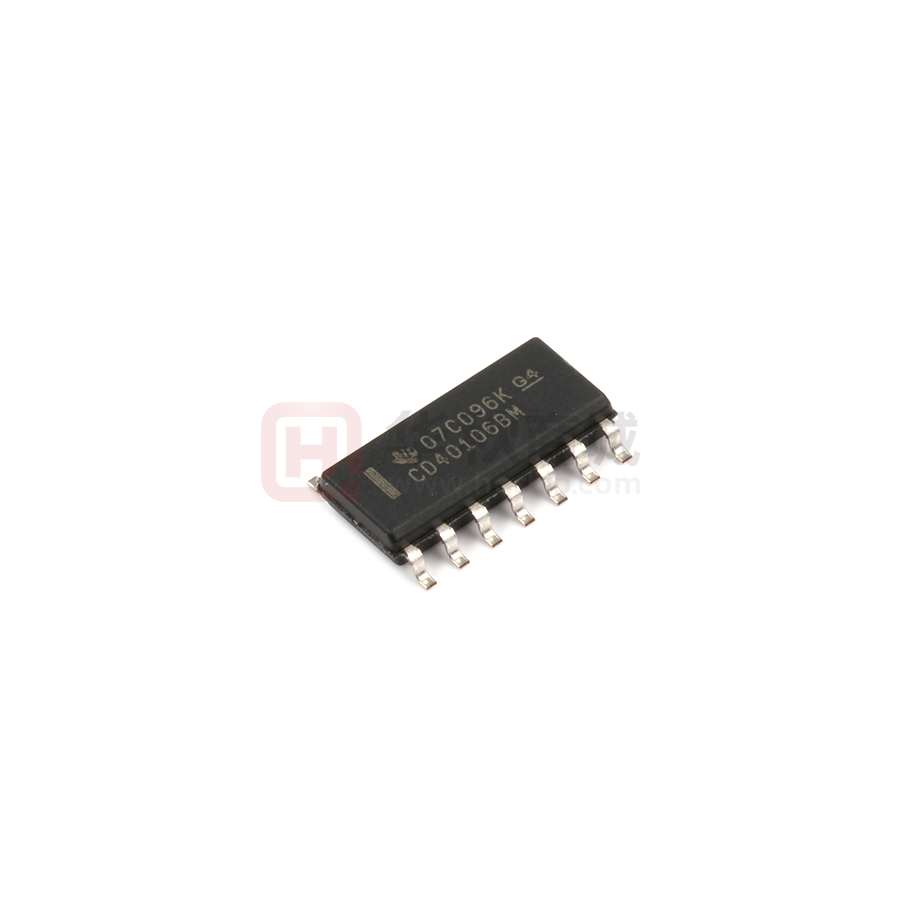
CD40106BM
SOIC (14)
3.90 mm x 8.65 mm
CD40106BNSR
SO (14)
5.30 mm x 10.20 mm
CD40106BPWR
TSSOP (14)
4.40 mm x 5.00 mm
(1) For all available packages, see the orderable addendum at
the end of the data sheet.
Logic Diagram
A
1 (3, 5, 9, 11, 13)
G
2 (4, 6, 8, 10, 12)
VDD
VSS
Copyright © 2017, Texas Instruments Incorporated
All inputs protected by the protection network shown to the right
1
An IMPORTANT NOTICE at the end of this data sheet addresses availability, warranty, changes, use in safety-critical applications,
intellectual property matters and other important disclaimers. PRODUCTION DATA.
�CD40106B
SCHS097F – NOVEMBER 1998 – REVISED MARCH 2017
www.ti.com
Table of Contents
1
2
3
4
5
6
7
8
Features ..................................................................
Applications ...........................................................
Description .............................................................
Revision History.....................................................
Pin Configuration and Functions .........................
Specifications.........................................................
1
1
1
2
3
4
6.1
6.2
6.3
6.4
6.5
6.6
6.7
4
4
4
4
5
8
9
Absolute Maximum Ratings ......................................
ESD Ratings ............................................................
Recommended Operating Conditions.......................
Thermal Information ..................................................
Electrical Characteristics: Static................................
Electrical Characteristics: Dynamic...........................
Typical Characteristics ..............................................
Parameter Measurement Information ................ 11
Detailed Description ............................................ 13
8.1 Overview ................................................................ 13
8.2 Functional Block Diagram ....................................... 13
8.3 Feature Description ................................................ 13
8.4 Device Functional Modes........................................ 13
9
Application and Implementation ........................ 14
9.1 Application Information .......................................... 14
9.2 Typical Applications ................................................ 14
10 Power Supply Recommendations ..................... 16
11 Layout................................................................... 16
11.1 Layout Guidelines ................................................ 16
11.2 Layout Example .................................................... 16
12 Device and Documentation Support ................. 18
12.1
12.2
12.3
12.4
12.5
Receiving Notification of Documentation Updates
Community Resources..........................................
Trademarks ...........................................................
Electrostatic Discharge Caution ............................
Glossary ................................................................
18
18
18
18
18
13 Mechanical, Packaging, and Orderable
Information ........................................................... 18
4 Revision History
NOTE: Page numbers for previous revisions may differ from page numbers in the current version.
Changes from Revision E (September 2016) to Revision F
•
Page
Changed incorrect pin descriptions to match package drawing ............................................................................................ 3
Changes from Revision D (August 2003) to Revision E
Page
•
Added ESD Ratings table, Feature Description section, Device Functional Modes, Application and Implementation
section, Power Supply Recommendations section, Layout section, Device and Documentation Support section, and
Mechanical, Packaging, and Orderable Information section .................................................................................................. 1
•
Added Thermal Information table ........................................................................................................................................... 4
2
Submit Documentation Feedback
Copyright © 1998–2017, Texas Instruments Incorporated
Product Folder Links: CD40106B
�CD40106B
www.ti.com
SCHS097F – NOVEMBER 1998 – REVISED MARCH 2017
5 Pin Configuration and Functions
D, J, N, NS, PW Packages
14-Pin SOIC, CDIP, PDIP, SO, TSSOP
Top View
G=
H=
I=
A
1
14
VDD
A
2
13
F
B
3
12
L=
B
4
11
E
C
5
10
K=
C
6
9
D
VSS
7
8
J=
F
E
D
Not to scale
Pin Functions
PIN
NO.
NAME
I/O
DESCRIPTION
1
A
I
Channel A input
2
G=A
O
Channel A inverted output
3
B
I
Channel B input
4
H=B
O
Channel B inverted output
5
C
I
Channel C input
6
I=C
O
Channel C inverted output
7
VSS
—
Ground
8
J=D
O
Channel D inverted output
9
D
I
Channel D input
10
K=E
O
Channel E inverted output
11
E
I
Channel E input
12
L=F
O
Channel F inverted output
13
F
I
Channel F input
14
VDD
—
Power supply
Submit Documentation Feedback
Copyright © 1998–2017, Texas Instruments Incorporated
Product Folder Links: CD40106B
3
�CD40106B
SCHS097F – NOVEMBER 1998 – REVISED MARCH 2017
www.ti.com
6 Specifications
6.1 Absolute Maximum Ratings
over operating free-air temperature range (unless otherwise noted) (1)
MIN
MAX
UNIT
DC supply voltage, VDD (2)
–0.5
20
V
Input voltage, all inputs
–0.5
VDD + 0.5
V
±10
mA
DC input current, any one input
TA = –55°C to +100°C
Power dissipation, PD
TA = 100°C to 125°C
500
(3)
mW
200
Device dissipation per output transistor
100
mW
Maximum junction temperature, TJ
150
°C
150
°C
Storage temperature, Tstg
(1)
(2)
(3)
–65
Stresses beyond those listed under Absolute Maximum Ratings may cause permanent damage to the device. These are stress ratings
only, which do not imply functional operation of the device at these or any other conditions beyond those indicated under Recommended
Operating Conditions. Exposure to absolute-maximum-rated conditions for extended periods may affect device reliability.
Voltages referenced to VSS terminal
Derate linearity at 12 mW/°C
6.2 ESD Ratings
VALUE
Electrostatic
discharge
V(ESD)
(1)
(2)
Human-body model (HBM), per ANSI/ESDA/JEDEC JS-001 (1)
2000
Charged-device model (CDM), per JEDEC specification JESD22-C101 (2)
1000
UNIT
V
JEDEC document JEP155 states that 500-V HBM allows safe manufacturing with a standard ESD control process.
JEDEC document JEP157 states that 250-V CDM allows safe manufacturing with a standard ESD control process.
6.3 Recommended Operating Conditions
over operating free-air temperature range (unless otherwise noted)
MIN
Supply voltage
Operating temperature, TA
MAX
UNIT
3
18
V
–55
125
°C
6.4 Thermal Information
CD40106B
THERMAL METRIC (1)
D (SOIC)
N (PDIP)
NS (SO)
PW (TSSOP)
14 PINS
14 PINS
14 PINS
14 PINS
UNIT
RθJA
Junction-to-ambient
thermal resistance
86.1
51.3
83.5
114.1
°C/W
RθJC(top)
Junction-to-case (top)
thermal resistance
44.3
38.6
41.5
39.1
°C/W
RθJB
Junction-to-board
thermal resistance
40.6
31.2
42.2
56.9
°C/W
ψJT
Junction-to-top
characterization parameter
11.6
23.4
13.1
3.1
°C/W
ψJB
Junction-to-board
characterization parameter
40.3
31.3
41.8
56.2
°C/W
(1)
4
For more information about traditional and new thermal metrics, see the Semiconductor and IC Package Thermal Metrics application
report.
Submit Documentation Feedback
Copyright © 1998–2017, Texas Instruments Incorporated
Product Folder Links: CD40106B
�CD40106B
www.ti.com
SCHS097F – NOVEMBER 1998 – REVISED MARCH 2017
6.5 Electrical Characteristics: Static
over operating free-air temperature range (unless otherwise noted)
PARAMETER
TEST CONDITIONS
MIN
TYP
TA = –55°C
VIN = 0 or 10, VDD = 10
IDDmax
Quiescent device current
1
TA = 25°C
0.02
VIN = 0 or 20, VDD = 20
VDD = 5
VPmin
Positive trigger threshold
voltage
VDD = 10
VDD = 15
1
TA = 85°C
30
TA = 125°C
30
TA = –55°C
2
TA = –40°C
2
TA = 25°C
0.02
2
TA = 85°C
60
TA = 125°C
60
TA = –55°C
4
TA = –40°C
VIN = 0 or 15, VDD = 15
UNIT
1
TA = –40°C
VIN = 0 or 5, VDD = 5
MAX
4
TA = 25°C
0.02
4
TA = 85°C
120
TA = 125°C
120
TA = –55°C
20
TA = –40°C
20
TA = 25°C
0.04
20
TA = 85°C
600
TA = 125°C
600
TA = –55°C
2.2
TA = –40°C
2.2
TA = 25°C
2.2
TA = 85°C
2.2
TA = 125°C
2.2
TA = –55°C
4.6
TA = –40°C
4.6
TA = 25°C
4.6
TA = 85°C
4.6
TA = 125°C
4.6
TA = –55°C
6.8
TA = –40°C
6.8
TA = 25°C
6.8
TA = 85°C
6.8
TA = 125°C
6.8
2.9
5.9
Product Folder Links: CD40106B
V
8.8
Submit Documentation Feedback
Copyright © 1998–2017, Texas Instruments Incorporated
µA
5
�CD40106B
SCHS097F – NOVEMBER 1998 – REVISED MARCH 2017
www.ti.com
Electrical Characteristics: Static (continued)
over operating free-air temperature range (unless otherwise noted)
PARAMETER
TEST CONDITIONS
MIN
TYP
TA = –55°C
VPmax
Positive trigger threshold
voltage
VDD = 10
3.6
TA = 25°C
2.9
3.6
TA = 125°C
3.6
TA = –55°C
7.1
TA = –40°C
7.1
TA = 25°C
5.9
7.1
TA = 125°C
7.1
TA = –55°C
10.8
Negative trigger threshold
voltage
VDD = 10
VDD = 15
8.8
10.8
TA = –55°C
0.9
TA = –40°C
0.9
TA = 25°C
0.9
TA = 85°C
0.9
TA = 125°C
0.9
TA = –55°C
2.5
TA = –40°C
2.5
TA = 25°C
2.5
TA = 85°C
2.5
TA = 125°C
2.5
TA = –55°C
4
TA = –40°C
4
TA = 25°C
4
TA = 85°C
4
TA = 125°C
4
1.9
3.9
VNmax
Negative trigger threshold
voltage
VDD = 10
2.8
2.8
1.9
6
2.8
TA = 85°C
2.8
TA = 125°C
2.8
TA = –55°C
5.2
TA = –40°C
5.2
TA = 25°C
3.9
5.2
TA = 85°C
5.2
TA = 125°C
5.2
TA = –55°C
7.4
TA = –40°C
VDD = 15
V
5.8
TA = –40°C
TA = 25°C
10.8
10.8
TA = –55°C
VDD = 5
TA = 25°C
V
7.4
5.8
7.4
TA = 85°C
7.4
TA = 125°C
7.4
Submit Documentation Feedback
V
10.8
TA = 25°C
TA = 125°C
VNmin
7.1
TA = 85°C
TA = 85°C
VDD = 5
3.6
TA = 85°C
TA = –40°C
VDD = 15
UNIT
3.6
TA = –40°C
VDD = 5
MAX
Copyright © 1998–2017, Texas Instruments Incorporated
Product Folder Links: CD40106B
�CD40106B
www.ti.com
SCHS097F – NOVEMBER 1998 – REVISED MARCH 2017
Electrical Characteristics: Static (continued)
over operating free-air temperature range (unless otherwise noted)
PARAMETER
TEST CONDITIONS
VDD = 5
VHmin
Hysteresis voltage
VDD = 10
VDD = 15
VDD = 5
MIN
TA = –55°C
0.3
TA = –40°C
0.3
TA = 25°C
0.3
TA = 85°C
0.3
TA = 125°C
0.3
TA = –55°C
1.2
TA = –40°C
1.2
TA = 25°C
1.2
TA = 85°C
1.2
TA = 125°C
1.2
TA = –55°C
1.6
TA = –40°C
1.6
TA = 25°C
1.6
TA = 85°C
1.6
TA = 125°C
1.6
TYP
2.3
Hysteresis voltage
VDD = 10
3.5
1.6
TA = –40°C
1.6
0.9
1.6
TA = 125°C
1.6
TA = –55°C
3.4
IOLmin
Output low (sink) current
3.4
2.3
VO = 0.5, VIN = 0 or 10,
VDD = 10
3.4
TA = 125°C
3.4
TA = –55°C
5
TA = –40°C
5
3.5
5
TA = 125°C
5
TA = –55°C
0.64
TA = –40°C
0.61
TA = 25°C
0.51
TA = 85°C
0.42
TA = 125°C
0.36
TA = –55°C
1.6
TA = –40°C
1.5
TA = 25°C
1.3
TA = 85°C
1.1
TA = 125°C
0.9
TA = –55°C
4.2
1
2.6
3.4
TA = 85°C
2.8
TA = 125°C
2.4
6.8
Submit Documentation Feedback
Product Folder Links: CD40106B
mA
4
TA = 25°C
Copyright © 1998–2017, Texas Instruments Incorporated
V
5
TA = 85°C
TA = –40°C
VO = 1.5, VIN = 0 or 15,
VDD = 15
3.4
TA = 85°C
TA = 25°C
VO = 0.4, VIN = 0 or 5,
VDD = 5
1.6
TA = 85°C
TA = 25°C
VDD = 15
V
TA = –55°C
TA = 25°C
UNIT
0.9
TA = –40°C
VHmax
MAX
7
�CD40106B
SCHS097F – NOVEMBER 1998 – REVISED MARCH 2017
www.ti.com
Electrical Characteristics: Static (continued)
over operating free-air temperature range (unless otherwise noted)
PARAMETER
TEST CONDITIONS
VO = 4.6, VIN = 0 or 5,
VDD = 5
VO = 2.5, VIN = 0 or 5,
VDD = 5
Output high (source)
current
IOHmin
VO = 9.5, VIN = 0 or 10,
VDD = 10
MIN
TA = –55°C
–0.64
TA = –40°C
–0.61
TA = 25°C
–0.51
TA = 85°C
–0.42
TA = 125°C
–0.36
TA = –55°C
–2
TA = –40°C
–1.8
TA = 25°C
–1.6
TA = 85°C
–1.3
TA = 125°C
–1.15
TA = –55°C
–1.6
TA = –40°C
–1.5
TA = 25°C
–1.3
TA = 85°C
–1.1
TA = 125°C
–0.9
TA = –55°C
–4.2
TA = –40°C
–4
VO = 13.5, VIN = 0 or 15,
TA = 25°C
VDD = 15
TA = 85°C
–3.4
VOHmin
IINmax
Low-level output voltage
High-level output voltage
Input current
MAX
–1
–3.2
mA
–2.6
–6.8
–2.4
VIN = 5, VDD = 5
TA = –55°C, –40°C,
25°C, 85°C, and 125°C
0
0.05
VIN = 10, VDD = 10
TA = –55°C, –40°C,
25°C, 85°C, and 125°C
0
0.05
VIN = 15, VDD = 15
TA = –55°C, –40°C,
25°C, 85°C, and 125°C
0
0.05
VIN = 0, VDD = 5
TA = –55°C, –40°C,
25°C, 85°C, and 125°C
4.95
5
VIN = 0, VDD = 10
TA = –55°C, –40°C,
25°C, 85°C, and 125°C
9.95
10
VIN = 0, VDD = 15
TA = –55°C, –40°C,
25°C, 85°C, and 125°C
14.95
15
VIN = 0 or 18, VDD = 18
UNIT
–2.8
TA = 125°C
VOLmax
TYP
V
TA = –55°C
±0.1
TA = –40°C
±0.1
TA = 25°C
±0.00001
V
±0.1
TA = 85°C
±1
TA = 125°C
±1
µA
6.6 Electrical Characteristics: Dynamic
at TA = 25°C, input tr, tf = 20 ns, CL = 50 pF, and RL = 200 kΩ (unless otherwise noted)
PARAMETER
tPHL,
tPLH
tTHL,
tTLH
CIN
8
Propagation delay time
Transition time
Input capacitance
TYP
MAX
VDD = 5
TEST CONDITIONS
140
280
VDD = 10
70
140
VDD = 15
60
120
VDD = 5
100
200
VDD = 10
50
100
VDD = 15
40
80
Any input
5
7.5
Submit Documentation Feedback
MIN
UNIT
ns
ns
pF
Copyright © 1998–2017, Texas Instruments Incorporated
Product Folder Links: CD40106B
�CD40106B
www.ti.com
SCHS097F – NOVEMBER 1998 – REVISED MARCH 2017
6.7 Typical Characteristics
20
40
Output Low (Sink) Current (mA)
35
Output Low (Sink) Current (mA)
Gate-to-Source Voltage = 5 V
Gate-to-Source Voltage = 10 V
Gate-to-Source Voltage = 15 V
30
25
20
15
10
5
Gate-to-Source Voltage = 5 V
Gate-to-Source Voltage = 10 V
Gate-to-Source Voltage = 15 V
17.5
15
12.5
10
7.5
5
2.5
0
0
0
5
10
15
Drain-to-Source Voltage (V)
20
0
25
5
D001
Figure 1. Typical Output Low (Sink)
Current Characteristics
Output High (Source) Current (mA)
Output High (Source) Current (mA)
-10
-15
-20
-25
-30
-35
-40
-25
-20
-15
-10
Drain-to-Source Voltage (V)
-5
-5
-10
-15
-20
-25
0
-20
D003
Output Voltage (V)
17.5
1.25
12.5
VDD
Current
Peak
10 V
VIN
Current
Peak
1
2
VO
1
0.75
ID
5V
5
1.75
VO
IO 1.5
All Other
Inputs to:
VDD or VSS
2.5
0
2.5
5
7.5
10
12.5
Input Voltage (V)
15
17.5
D004
0.5
-55°C
125°C
VDD
10 V
10
VIN
7.5
1
5V
5
0
20
2
VO
All Other
Inputs to:
VDD or VSS
2.5
0
0
2.5
D016
Figure 5. Typical Current and Voltage
Transfer Characteristics
0
VDD = 15 V
0.25
0
-5
15
Output Voltage (V)
VDD = 15 V
-15
-10
Drain-to-Source Voltage (V)
Figure 4. Minimum Output High (Source)
Current Characteristics
Drain Current (mA)
17.5
7.5
D002
Gate-to-Source Voltage = -5 V
Gate-to-Source Voltage = -10 V
Gate-to-Source Voltage = -15 V
Figure 3. Typical Output High (Source)
Current Characteristics
10
25
0
Gate-to-Source Voltage = -5 V
Gate-to-Source Voltage = -10 V
Gate-to-Source Voltage = -15 V
-5
12.5
20
Figure 2. Minimum Output Low (Sink)
Current Characteristics
0
15
10
15
Drain-to-Source Voltage (V)
5
7.5
10 12.5 15
Input Voltage (V)
17.5
20
22.5
D017
Figure 6. Typical Voltage Transfer Characteristics as a
Function of Temperature
Submit Documentation Feedback
Copyright © 1998–2017, Texas Instruments Incorporated
Product Folder Links: CD40106B
9
�CD40106B
SCHS097F – NOVEMBER 1998 – REVISED MARCH 2017
www.ti.com
Typical Characteristics (continued)
300
200
Propagation Delay Time (ns)
Supply Voltage = 5 V
Supply Voltage = 10 V
Supply Voltage = 15 V
Supply Voltage = 5 V
Supply Voltage = 10 V
Supply Voltage = 15 V
250
Transition Time (ns)
150
100
50
200
150
100
50
0
0
0
10
20
30
40
50
60
70
Load Capacitance (pF)
80
90
100
0
Figure 7. Typical Propagation Delay Time as a
Function of Load Capacitance
40
60
80
100
Load Capacitance (pF)
120
140
D010
Figure 8. Typical Transition Time as a
Function of Load Capacitance
20
100k
VP
VN
VDD = 5 V (CL = 50 pF)
VDD = 10 V (CL = 15 pF)
VDD = 10 V (CL = 50 pF)
VDD = 15 V (CL = 50 pF)
10k
Trigger Threshold Voltage (V)
Power Dissipation Per Trigger (PW)
20
D018
1k
100
10
100m
15
10
5
0
1
10
100
Input Frequency (kHz)
1k
10k
0
5
D019
Figure 9. Typical Power Dissipation Per Trigger as a
Function of Input Frequency
10
15
Supply Voltage (V)
20
25
D020
Figure 10. Typical Trigger Threshold Voltage as a
Function of Supply Voltage
Hysteresis [V H/VDD u 100] (%)
35
30
25
20
15
10
5
0
0
5
10
15
Supply Voltage (V)
20
22.5
D021
Figure 11. Typical Percent Hysteresis as a Function of Supply Voltage
10
Submit Documentation Feedback
Copyright © 1998–2017, Texas Instruments Incorporated
Product Folder Links: CD40106B
�CD40106B
www.ti.com
SCHS097F – NOVEMBER 1998 – REVISED MARCH 2017
7 Parameter Measurement Information
VOH
VOL
Loa d
Driver
Output
Characteristic
Input
Characteristic
VDD
Log ic 1
Output
Region
Log ic 1
Input
Region
VP
VOH
VN
Log ic 0
Output
Region
Log ic 0
Input
Region
VOL
VSS
Figure 12. Input and Output Characteristics
VP
VN
VDD
VO
VIN
VH
VIN
VO
VH = VP ± VN
VH
VSS
VIN
VDD
VN
VP
VO
VSS
a) Definition of VP, VN, and VH
b) Transfer Characteristics of 1 of 6 Gates
Figure 13. Hysteresis Definition, Characteristics, and Test Set-Up
VDD
VDD
INPUTS
VSS
IDD
VSS
Figure 14. Quiescent Device Current Test Circuit
Submit Documentation Feedback
Copyright © 1998–2017, Texas Instruments Incorporated
Product Folder Links: CD40106B
11
�CD40106B
SCHS097F – NOVEMBER 1998 – REVISED MARCH 2017
www.ti.com
Parameter Measurement Information (continued)
VDD
INPUTS
VDD
I
VSS
VSS
Figure 15. Input Current Test Circuit
VDD
Pulse
Gen erator
0.1 F
IDD
500 F
2
1
CL
VSS
Figure 16. Dynamic Power Dissipation Test Circuit
12
Submit Documentation Feedback
Copyright © 1998–2017, Texas Instruments Incorporated
Product Folder Links: CD40106B
�CD40106B
www.ti.com
SCHS097F – NOVEMBER 1998 – REVISED MARCH 2017
8 Detailed Description
8.1 Overview
The CD40106B device contains six independent inverters with schmitt trigger inputs.. They perform the Boolean
function Y = A in positive logic.
Schmitt-Trigger inputs are designed to provide a minimum separation between positive and negative switching
thresholds. This allows for noisy or slow inputs that would cause problems such as oscillation or excessive
current consumption.
8.2 Functional Block Diagram
A
B
C
D
E
F
1
2
3
4
5
6
9
8
11
10
13
12
G=A
H=B
I=C
J=D
K=E
L=F
VDD = Pin 14
VSS = Pin 7
Copyright © 2017, Texas Instruments Incorporated
8.3 Feature Description
The CD40106B has standardized symmetrical output characteristics and a wide operating voltage from 3 V to
18 V with quiescent current of 20 µA tested at 20 V. These devices have transition times of tTLH = tTHL = 50 ns
(typical) at 10 V. The operating temperature is from –55°C to +125°C. Schmitt trigger inputs on this device
support slow or noisy input signals.
8.4 Device Functional Modes
Table 1 lists the functional modes of the CD40106B.
Table 1. Function Table
INPUT
OUTPUT
H
L
L
H
Submit Documentation Feedback
Copyright © 1998–2017, Texas Instruments Incorporated
Product Folder Links: CD40106B
13
�CD40106B
SCHS097F – NOVEMBER 1998 – REVISED MARCH 2017
www.ti.com
9 Application and Implementation
NOTE
Information in the following applications sections is not part of the TI component
specification, and TI does not warrant its accuracy or completeness. TI’s customers are
responsible for determining suitability of components for their purposes. Customers should
validate and test their design implementation to confirm system functionality.
9.1 Application Information
The CD40106B device is a Schmitt-Trigger input device that can be used for a multitude of inverting buffer type
functions. The application shown here takes advantage of the Schmitt-Trigger inputs to produce a square wave
output from a sine wave input.
9.2 Typical Applications
9.2.1 Wave Shaper
VDD
VDD
VSS
VSS
1/6 CD40106B
Frequency Range of Wave Shape
is from DC to 1 MHz.
Copyright © 2017, Texas Instruments Incorporated
Figure 17. Wave Shaper Schematic
9.2.1.1 Design Requirements
Take care to avoid bus contention, because it can drive currents that would exceed maximum limits. Parallel
output drive can create fast edges into light loads so consider routing and load conditions to prevent ringing.
9.2.1.2 Detailed Design Procedure
The recommended input conditions for Figure 17 includes specified high and low levels (see VP and VN in
Electrical Characteristics: Static). Inputs are not overvoltage tolerant and must be below VCC level because of the
presence of input clamp diodes to VCC.
The recommended output condition for the CD40106B application includes specific load currents. Load currents
must be limited so as to not exceed the total power (continuous current through VCC or GND) for the device.
These limits are in the Absolute Maximum Ratings. Outputs must not be pulled above VCC.
9.2.1.3 Application Curve
1M
Power Dissipation (PW)
100k
VDD = 5 V (f = 1 kHz)
VDD = 10 V (f = 1 kHz)
VDD = 15 V (f = 1 kHz)
VDD = 15 V (f = 10 kHz)
VDD = 15 V (f = 100 kHz)
10k
1k
100
10
1
100m
10
100
1k
10k
Rise and Fall Time (ns)
100k
1M
D022
Figure 18. Typical Power Dissipation as a Function of Rise and Fall Times
14
Submit Documentation Feedback
Copyright © 1998–2017, Texas Instruments Incorporated
Product Folder Links: CD40106B
�CD40106B
www.ti.com
SCHS097F – NOVEMBER 1998 – REVISED MARCH 2017
Typical Applications (continued)
9.2.2 Monostable Multivibrator
The timing of the monostable multivibrator circuit can be set by following the equations shown in Figure 19.
VDD
tM
R
VDD
1/3 CD4007UB
1
2
VDD
VSS
C
1/6 CD40106B
VSS
æ VDD
ö
tM = RC l n ç
÷
è VDD - VP ø
50 kW £ R £ 1MW
VSS
100 pF £ C £ 1 mF
For the Range of R and C
Given 5 ms < tM < 1 s
Copyright © 2016, Texas Instruments Incorporated
Figure 19. Monostable Multivibrator Schematic and Equations
9.2.3 Astable Multivibrator
The timing of the astable multivibrator circuit can be set by following the equations shown in Figure 20.
tA
1/6 CD40106B
VDD
VSS
R
C
VSS
éæ V ö æ V - VN ö ù
t A = RC l n êç P ÷ ç DD
÷ú
êëè VN ø è VDD - VP ø úû
50 kW £ R £ 1MW
100 pF £ C £ 1 mF
For the Range of R and C
Given 2 ms < t A < 0.4 s
Copyright © 2016, Texas Instruments Incorporated
Figure 20. Astable Multivibrator Schematic and Equations
Submit Documentation Feedback
Copyright © 1998–2017, Texas Instruments Incorporated
Product Folder Links: CD40106B
15
�CD40106B
SCHS097F – NOVEMBER 1998 – REVISED MARCH 2017
www.ti.com
10 Power Supply Recommendations
The power supply can be any voltage between the minimum and maximum supply voltage rating located in the
Recommended Operating Conditions. The VCC terminal must have a good bypass capacitor to prevent power
disturbance. A 0.1-µF capacitor is recommended to be used on the VCC terminal, and it must be placed as close
as possible to the pin for best results.
11 Layout
11.1 Layout Guidelines
When using multiple bit logic devices, inputs must never float. In many cases, functions or parts of functions of
digital logic devices are unused, for example, when only two inputs of a triple-input AND gate are used or only
three of the four buffer gates are used. Such inputs must not be left unconnected because the undefined
voltages at the outside connections result in undefined operational states. All unused inputs of digital logic
devices must be connected to a high or low bias to prevent them from floating. The logic level that must be
applied to any particular unused input depends on the function of the device. Generally they are tied to GND or
VCC, whichever makes more sense or is more convenient. Floating outputs are generally acceptable, unless the
part is a transceiver.
11.2 Layout Example
Vcc
Unused Input
Input
Output
Unused Input
Output
Input
Figure 21. Layout Diagram
16
Submit Documentation Feedback
Copyright © 1998–2017, Texas Instruments Incorporated
Product Folder Links: CD40106B
�CD40106B
www.ti.com
SCHS097F – NOVEMBER 1998 – REVISED MARCH 2017
Layout Example (continued)
0
10
20
30
40
50 53
76
70
60
50
40
73±81
(1.854±2.057)
30
20
10
0
4±10
(0.102±0.254)
50±58
(1.270±1.473)
Figure 22. Dimensions and Pad Layout for CD40106BH
Submit Documentation Feedback
Copyright © 1998–2017, Texas Instruments Incorporated
Product Folder Links: CD40106B
17
�CD40106B
SCHS097F – NOVEMBER 1998 – REVISED MARCH 2017
www.ti.com
12 Device and Documentation Support
12.1 Receiving Notification of Documentation Updates
To receive notification of documentation updates, navigate to the device product folder on ti.com. In the upper
right corner, click on Alert me to register and receive a weekly digest of any product information that has
changed. For change details, review the revision history included in any revised document.
12.2 Community Resources
The following links connect to TI community resources. Linked contents are provided "AS IS" by the respective
contributors. They do not constitute TI specifications and do not necessarily reflect TI's views; see TI's Terms of
Use.
TI E2E™ Online Community TI's Engineer-to-Engineer (E2E) Community. Created to foster collaboration
among engineers. At e2e.ti.com, you can ask questions, share knowledge, explore ideas and help
solve problems with fellow engineers.
Design Support TI's Design Support Quickly find helpful E2E forums along with design support tools and
contact information for technical support.
12.3 Trademarks
E2E is a trademark of Texas Instruments.
All other trademarks are the property of their respective owners.
12.4 Electrostatic Discharge Caution
These devices have limited built-in ESD protection. The leads should be shorted together or the device placed in conductive foam
during storage or handling to prevent electrostatic damage to the MOS gates.
12.5 Glossary
SLYZ022 — TI Glossary.
This glossary lists and explains terms, acronyms, and definitions.
13 Mechanical, Packaging, and Orderable Information
The following pages include mechanical, packaging, and orderable information. This information is the most
current data available for the designated devices. This data is subject to change without notice and revision of
this document. For browser-based versions of this data sheet, refer to the left-hand navigation.
18
Submit Documentation Feedback
Copyright © 1998–2017, Texas Instruments Incorporated
Product Folder Links: CD40106B
�PACKAGE OPTION ADDENDUM
www.ti.com
13-Aug-2021
PACKAGING INFORMATION
Orderable Device
Status
(1)
Package Type Package Pins Package
Drawing
Qty
Eco Plan
(2)
Lead finish/
Ball material
MSL Peak Temp
Op Temp (°C)
Device Marking
(3)
(4/5)
(6)
CD40106BE
ACTIVE
PDIP
N
14
25
RoHS & Green
NIPDAU
N / A for Pkg Type
-55 to 125
CD40106BE
CD40106BEE4
ACTIVE
PDIP
N
14
25
RoHS & Green
NIPDAU
N / A for Pkg Type
-55 to 125
CD40106BE
CD40106BF
ACTIVE
CDIP
J
14
1
Non-RoHS
& Green
SNPB
N / A for Pkg Type
-55 to 125
CD40106BF
CD40106BF3A
ACTIVE
CDIP
J
14
1
Non-RoHS
& Green
SNPB
N / A for Pkg Type
-55 to 125
CD40106BF3A
CD40106BM
ACTIVE
SOIC
D
14
50
RoHS & Green
NIPDAU
Level-1-260C-UNLIM
-55 to 125
CD40106BM
CD40106BM96
ACTIVE
SOIC
D
14
2500
RoHS & Green
NIPDAU
Level-1-260C-UNLIM
-55 to 125
CD40106BM
CD40106BM96E4
ACTIVE
SOIC
D
14
2500
RoHS & Green
NIPDAU
Level-1-260C-UNLIM
-55 to 125
CD40106BM
CD40106BM96G4
ACTIVE
SOIC
D
14
2500
RoHS & Green
NIPDAU
Level-1-260C-UNLIM
-55 to 125
CD40106BM
CD40106BMG4
ACTIVE
SOIC
D
14
50
RoHS & Green
NIPDAU
Level-1-260C-UNLIM
-55 to 125
CD40106BM
CD40106BMT
ACTIVE
SOIC
D
14
250
RoHS & Green
NIPDAU
Level-1-260C-UNLIM
-55 to 125
CD40106BM
CD40106BNSR
ACTIVE
SO
NS
14
2000
RoHS & Green
NIPDAU
Level-1-260C-UNLIM
-55 to 125
CD40106B
CD40106BPW
ACTIVE
TSSOP
PW
14
90
RoHS & Green
NIPDAU
Level-1-260C-UNLIM
-55 to 125
CM0106B
CD40106BPWR
ACTIVE
TSSOP
PW
14
2000
RoHS & Green
NIPDAU
Level-1-260C-UNLIM
-55 to 125
CM0106B
(1)
The marketing status values are defined as follows:
ACTIVE: Product device recommended for new designs.
LIFEBUY: TI has announced that the device will be discontinued, and a lifetime-buy period is in effect.
NRND: Not recommended for new designs. Device is in production to support existing customers, but TI does not recommend using this part in a new design.
PREVIEW: Device has been announced but is not in production. Samples may or may not be available.
OBSOLETE: TI has discontinued the production of the device.
(2)
RoHS: TI defines "RoHS" to mean semiconductor products that are compliant with the current EU RoHS requirements for all 10 RoHS substances, including the requirement that RoHS substance
do not exceed 0.1% by weight in homogeneous materials. Where designed to be soldered at high temperatures, "RoHS" products are suitable for use in specified lead-free processes. TI may
reference these types of products as "Pb-Free".
RoHS Exempt: TI defines "RoHS Exempt" to mean products that contain lead but are compliant with EU RoHS pursuant to a specific EU RoHS exemption.
Addendum-Page 1
Samples
�PACKAGE OPTION ADDENDUM
www.ti.com
13-Aug-2021
Green: TI defines "Green" to mean the content of Chlorine (Cl) and Bromine (Br) based flame retardants meet JS709B low halogen requirements of


 工商网监
湘ICP备2023018690号
工商网监
湘ICP备2023018690号

