CD4504B-EP
www.ti.com .......................................................................................................................................................................................... SCHS369 – NOVEMBER 2008
CMOS HEX VOLTAGE-LEVEL SHIFTER
FOR TTL-TO-CMOS or CMOS-TO-CMOS OPERATION
FEATURES
1
•
•
•
•
•
•
•
•
Independence of Power-Supply Sequence
Considerations – VCC Can Exceed VDD;
Input Signals Can Exceed Both VCC and VDD
Up and Down Level-Shifting Capability
Shiftable Input Threshold for Either CMOS or
TTL Compatibility
Standardized Symmetrical Output
Characteristics
100% Tested for Quiescent Current at 20 V
Maximum Input Current of 1 µA at 18 V Over
Full Package-Temperature Range:
100 nA at 18 V and 25°C
5 V, 10 V, and 15 V Parametric Ratings
Meets All Requirements of JEDEC Standard
No. 13B, "Standard Specifications for
Description of 'B' Series CMOS Devices"
SUPPORTS DEFENSE, AEROSPACE,
AND MEDICAL APPLICATIONS
•
•
•
•
•
•
•
Controlled Baseline
One Assembly/Test Site
One Fabrication Site
Available in Military (–55°C/125°C)
Temperature Range (1)
Extended Product Life Cycle
Extended Product-Change Notification
Product Traceability
(TO P V IE W )
VCC
1
16
VDD
AOUT
2
15
FOUT
AIN
3
14
FIN
BOUT
4
13
SELECT
BIN
5
12
EOUT
COUT
6
11
EIN
7
10
DOUT
8
9
CIN
VSS
(1)
DIN
Additional temperature ranges are available – contact factory
DESCRIPTION
CD4504B hex voltage level-shifter consists of six circuits which shift input signals from the VCC logic level to the
VDD logic level. To shift TTL signals to CMOS logic levels, the SELECT input is at the VCC HIGH logic state.
When the SELECT input is at a LOW logic state, each circuit translates signals from one CMOS level to another.
ORDERING INFORMATION (1)
PACKAGE (2)
TA
–55°C to 125°C
(1)
(2)
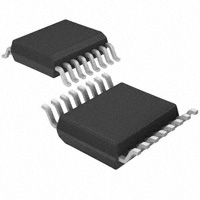
TSSOP – PW
Reel of 2000
ORDERABLE PART NUMBER
CD4504BMPWREP
TOP-SIDE MARKING
4504BEP
Package drawings, thermal data, and symbolization are available at www.ti.com/packaging.
For the most current package and ordering information, see the Package Option Addendum at the end of this document, or see the TI
website at www.ti.com.
1
Please be aware that an important notice concerning availability, standard warranty, and use in critical applications of Texas
Instruments semiconductor products and disclaimers thereto appears at the end of this data sheet.
PRODUCTION DATA information is current as of publication date.
Products conform to specifications per the terms of the Texas
Instruments standard warranty. Production processing does not
necessarily include testing of all parameters.
Copyright © 2008, Texas Instruments Incorporated
�CD4504B-EP
SCHS369 – NOVEMBER 2008 .......................................................................................................................................................................................... www.ti.com
FUNCTIONAL BLOCK DIAGRAM
ABSOLUTE MAXIMUM RATINGS
over operating free-air temperature range (unless otherwise noted)
VDD
MIN
MAX
UNIT
DC supply-voltage range, voltages referenced to VSS terminal
–0.5
+20
V
Input voltage range, all inputs
–0.5
VCC + 0.5
DC input current, any one input
TA = –55°C to +100°C
PD
Power dissipation per package
Operating temperature range
θJA
Package thermal impedance (1)
Tstg
Storage temperature range
2
500
mW
100
–55
–85
Lead temperature (during soldering), at distance 1/16 ± 1/32 inch (1.59 ± 0.79 mm) from case for
10 s max
(1)
mA
Derate Linearly at 12 mW/°C to
200 nW
TA = +100°C to +125°C
Device dissipation per output transistor,
for TA = full package-temperature range (all package types)
TA
V
±10
mW
+125
°C
91.1
°C/W
+150
°C
+265
°C
The package thermal impedance is calculated in accordance with JESD 51-7.
Submit Documentation Feedback
Copyright © 2008, Texas Instruments Incorporated
Product Folder Link(s): CD4504B-EP
�CD4504B-EP
www.ti.com .......................................................................................................................................................................................... SCHS369 – NOVEMBER 2008
STATIC ELECTRICAL CHARACTERISTICS
over operating free-air temperature range (unless otherwise noted)
CONDITIONS
CHARACTERISTIC
VO
(V)
Quiescent device current,
IDD max and ICC in CMOS-CMOS mode
Quiescent device current,
ICC max TTL-CMOS mode
Output low (sink) current,
IOL min
Output high (source) current,
IOH min
–55
–40
+85
+125
+25
MIN
UNIT
TYP
MAX
0, 5
5
5
1.5
1.5
1.5
1.5
0.02
1.5
0, 10
5
10
2
2
2
2
0.02
2
0, 15
5
15
4
4
120
120
0.02
4
0, 20
5
20
20
20
600
600
0.04
20
0, 5
5
5
5
5
6
6
2.5
5
0, 10
5
10
5
5
6
6
2.5
5
0, 15
5
2.5
5
15
5
5
6
6
5
0.64
0.61
0.42
0.36
0.51
1
0.5
0, 10
10
1.6
1.5
1.1
0.9
1.3
2.6
1.5
0, 15
15
4.2
4
2.8
2.4
3.4
6.8
4.6
0, 5
5
–0.64
–0.61
–0.42
–0.36
–0.51
–1
2.5
0, 5
5
–2
–1.8
–1.3
–1.15
–1.6
–3.2
9.5
0, 10
10
–1.6
–1.5
–1.1
–0.9
–1.3
–2.6
13.5
0, 15
15
–4.2
–4
–2.8
–2.4
–3.4
–6.8
0, 5
5
0.05
0
0.05
0, 10
10
0.05
0
0.05
0, 15
15
0.05
0
0.05
0, 5
5
4.95
0, 10
10
0, 15
15
4.95
5
9.95
9.95
10
14.95
14.95
15
1
5
10
0.8
0.8
TTL-CMOS
1
5
15
0.8
0.8
CMOS-CMOS
1
5
10
1.5
1.5
CMOS-CMOS
1.5
5
15
1.5
1.5
CMOS-CMOS
1.5
10
15
3
TTL-CMOS
9
5
10
2
TTL-CMOS
5
15
2
2
9
5
10
3.5
3.5
CMOS-CMOS
13.5
5
15
3.5
3.5
CMOS-CMOS
13.5
10
15
7
7
±0.1
±0.1
mA
V
3
13.5
18
µA
2
CMOS-CMOS
0, 18
mA
mA
TTL-CMOS
Input current, IIN max
(1)
VCC
(V)
0, 5
Output voltage:
high-level, VOH min
Input high voltage,
VIH min (1)
VCC
(V)
0.4
Output voltage:
low-level, VOL max
Input low voltage,
VIL max (1)
VIN
(V)
LIMITS AT INDICATED TEMPERATURES (°C)
±1
±1
±10–5
±0.1
µA
Applies to the six input signals. For mode control (P13), only the CMOS-CMOS ratings apply.
Submit Documentation Feedback
Copyright © 2008, Texas Instruments Incorporated
Product Folder Link(s): CD4504B-EP
3
�CD4504B-EP
SCHS369 – NOVEMBER 2008 .......................................................................................................................................................................................... www.ti.com
Figure 1. Typical Output Low (sink) Current Characteristics
Figure 2. Minimum Output Low (sink) Current Characteristics
Figure 3. Typical Output High (source) Current Characteristics
4
Submit Documentation Feedback
Copyright © 2008, Texas Instruments Incorporated
Product Folder Link(s): CD4504B-EP
�CD4504B-EP
www.ti.com .......................................................................................................................................................................................... SCHS369 – NOVEMBER 2008
Figure 4. Minimum Output High (source) Current Characteristics
Submit Documentation Feedback
Copyright © 2008, Texas Instruments Incorporated
Product Folder Link(s): CD4504B-EP
5
�CD4504B-EP
SCHS369 – NOVEMBER 2008 .......................................................................................................................................................................................... www.ti.com
RECOMMENDED OPERATING CONDITIONS
For maximum reliability, nominal operating conditions should be selected so that operation is always within the following
ranges:
CHARACTERISTIC
VDD
Supply-voltage range (for TA = full package temperature range)
MIN
MAX
5
18
UNIT
V
DYNAMIC ELECTRICAL CHARACTERISTICS
TA = 25°C, Input tr,tf = 20 ns, CL = 50 pF, RL = 200 Ω
CHARACTERISTIC
SHIFTING MODE
TTL to CMOS
VDD > VCC
tPHL
Propagation delay: high-to-low,
CMOS to CMOS
VDD > VCC
CMOS to CMOS
VCC > VDD
TTL to CMOS
VDD > VCC
tPLH
Propagation delay: low-to-high
CMOS to CMOS
VDD > VCC
CMOS to CMOS
VCC > VDD
tTHL, tTLH
CIN
Transition time
Input capacitance
All modes
Any input
LIMITS
VCC
(V)
VDD
(V)
TYP
5
10
140
280
5
15
140
280
5
10
120
240
5
15
120
240
10
15
70
140
10
5
275
550
15
5
275
550
15
10
70
140
5
10
140
280
5
15
140
280
5
10
120
240
5
15
120
240
10
15
70
140
10
5
200
400
15
5
200
400
15
10
60
120
5
100
200
10
50
100
15
40
80
5
7.5
MAX
UNIT
ns
ns
ns
pF
Figure 5. Quiescent Device Current
6
Submit Documentation Feedback
Copyright © 2008, Texas Instruments Incorporated
Product Folder Link(s): CD4504B-EP
�CD4504B-EP
www.ti.com .......................................................................................................................................................................................... SCHS369 – NOVEMBER 2008
Figure 6. Input Current
Figure 7. Input Voltage
Figure 8. Typical Input Switching as a Function of
High-Level Supply Voltage (SELECT at VCC – CMOS
Mode
Figure 9. Typical Input Switching as a Function of
High-Level Supply Voltage (SELECT at VSS – TTL Mode)
Submit Documentation Feedback
Copyright © 2008, Texas Instruments Incorporated
Product Folder Link(s): CD4504B-EP
7
�CD4504B-EP
SCHS369 – NOVEMBER 2008 .......................................................................................................................................................................................... www.ti.com
Figure 10. High-Level Supply Voltage vs. Low-Level
Supply Voltage
A.
Dimensions in parentheses are in millimeters and are derived form the basic inch dimensions as indicated. Grid
graduations are in mils (10–3 inch).
Figure 11. Dimensions and Pad Layout
8
Submit Documentation Feedback
Copyright © 2008, Texas Instruments Incorporated
Product Folder Link(s): CD4504B-EP
�PACKAGE OPTION ADDENDUM
www.ti.com
10-Dec-2020
PACKAGING INFORMATION
Orderable Device
Status
(1)
Package Type Package Pins Package
Drawing
Qty
Eco Plan
(2)
Lead finish/
Ball material
MSL Peak Temp
Op Temp (°C)
Device Marking
(3)
(4/5)
(6)
CD4504BMPWREP
ACTIVE
TSSOP
PW
16
2000
RoHS & Green
NIPDAU
Level-1-260C-UNLIM
-55 to 125
4504BEP
V62/09606-01XE
ACTIVE
TSSOP
PW
16
2000
RoHS & Green
NIPDAU
Level-1-260C-UNLIM
-55 to 125
4504BEP
(1)
The marketing status values are defined as follows:
ACTIVE: Product device recommended for new designs.
LIFEBUY: TI has announced that the device will be discontinued, and a lifetime-buy period is in effect.
NRND: Not recommended for new designs. Device is in production to support existing customers, but TI does not recommend using this part in a new design.
PREVIEW: Device has been announced but is not in production. Samples may or may not be available.
OBSOLETE: TI has discontinued the production of the device.
(2)
RoHS: TI defines "RoHS" to mean semiconductor products that are compliant with the current EU RoHS requirements for all 10 RoHS substances, including the requirement that RoHS substance
do not exceed 0.1% by weight in homogeneous materials. Where designed to be soldered at high temperatures, "RoHS" products are suitable for use in specified lead-free processes. TI may
reference these types of products as "Pb-Free".
RoHS Exempt: TI defines "RoHS Exempt" to mean products that contain lead but are compliant with EU RoHS pursuant to a specific EU RoHS exemption.
Green: TI defines "Green" to mean the content of Chlorine (Cl) and Bromine (Br) based flame retardants meet JS709B low halogen requirements of