CD54HC245, CD74HC245, CD54HCT245, CD74HCT245
ZHCSQV5B – NOVEMBER 1998 – REVISED JULY 2022
CDx4HC(T)245 三态同相高速 CMOS 逻辑八路总线收发器
1 特性
2 说明
•
•
•
•
CDx4HC(T)245 是一款具有三态输出的八路总线收发
器。所有八个通道均由方向 (DIR) 引脚和输出使能
(OE) 引脚控制。
•
•
•
•
•
•
缓冲输入
三态输出
总线驱动能力
当 VCC = 5V、CL = 15pF、TA = 25°C 时,传播延
迟典型值(A 到 B,B 到 A)为 9ns
扇出(在温度范围内)
– 总线驱动器输出:15 个 LSTTL 负载
宽工作温度范围:-55°C 至 125°C
平衡的传播延迟及转换时间
与 LSTTL 逻辑 IC 相比,功耗显著降低
HC 类型
– 2 V 至 6 V 工作电压
– 高抗噪性:当 VCC = 5V 时,NIL = 30%,NIH =
VCC 的 30%
HCT 类型
– 工作电压为 4.5 V 至 5.5 V
– 直接 LSTTL 输入逻辑兼容性,VIL = 0.8V(最大
值),VIH = 2V(最小值)
– CMOS 输入兼容性,当电压为 VOL、VOH 时,Il
≤ 1µA
器件信息
(1)
器件型号
封装
CD54HC245F
J(CDIP、20) 26.92mm × 6.92mm
CD74HC245
N(PDIP、20) 25.40mm × 6.35mm
DW(SOIC、
20)
封装尺寸(标称值)
12.80mm × 7.50mm
CD54HCT245F
J(CDIP、20) 26.92mm × 6.92mm
CD74HCT245
N(PDIP、20) 25.40mm × 6.35mm
DW(SOIC、
20)
(1)
12.80mm × 7.50mm
如需了解所有封装,请参阅数据表末尾的可订购产品附录。
功能框图
本文档旨在为方便起见,提供有关 TI 产品中文版本的信息,以确认产品的概要。有关适用的官方英文版本的最新信息,请访问
www.ti.com,其内容始终优先。TI 不保证翻译的准确性和有效性。在实际设计之前,请务必参考最新版本的英文版本。
English Data Sheet: SCHS119
�CD54HC245, CD74HC245, CD54HCT245, CD74HCT245
www.ti.com.cn
ZHCSQV5B – NOVEMBER 1998 – REVISED JULY 2022
Table of Contents
1 特性................................................................................... 1
2 说明................................................................................... 1
3 Revision History.............................................................. 2
4 Pin Configuration and Functions...................................3
5 Specifications.................................................................. 4
5.1 Absolute Maximum Ratings........................................ 4
5.2 Recommended Operating Conditions.........................4
5.3 Thermal Information....................................................4
5.4 Electrical Characteristics.............................................5
5.5 Switching Characteristics............................................6
6 Parameter Measurement Information............................ 7
7 Detailed Description........................................................8
7.1 Overview..................................................................... 8
7.2 Device Functional Modes............................................8
8 Power Supply Recommendations..................................9
9 Layout...............................................................................9
9.1 Layout Guidelines....................................................... 9
10 Device and Documentation Support..........................10
10.1 Documentation Support.......................................... 10
10.2 接收文档更新通知................................................... 10
10.3 支持资源..................................................................10
10.4 Trademarks............................................................. 10
10.5 Electrostatic Discharge Caution..............................10
10.6 术语表..................................................................... 10
11 Mechanical, Packaging, and Orderable
Information.................................................................... 10
3 Revision History
注:以前版本的页码可能与当前版本的页码不同
Changes from Revision A (April 2003) to Revision B (July 2022)
Page
• 更新了整个文档中的编号、格式、表格、图和交叉参考,以反映现代数据表标准.............................................. 1
2
Submit Document Feedback
Copyright © 2022 Texas Instruments Incorporated
Product Folder Links: CD54HC245 CD74HC245 CD54HCT245 CD74HCT245
�CD54HC245, CD74HC245, CD54HCT245, CD74HCT245
www.ti.com.cn
ZHCSQV5B – NOVEMBER 1998 – REVISED JULY 2022
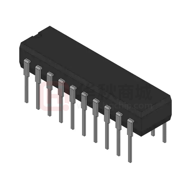
4 Pin Configuration and Functions
J, N and DW Package
20-Pin CDIP, PDIP or SOIC
Top View
Copyright © 2022 Texas Instruments Incorporated
Submit Document Feedback
Product Folder Links: CD54HC245 CD74HC245 CD54HCT245 CD74HCT245
3
�CD54HC245, CD74HC245, CD54HCT245, CD74HCT245
www.ti.com.cn
ZHCSQV5B – NOVEMBER 1998 – REVISED JULY 2022
5 Specifications
5.1 Absolute Maximum Ratings
over operating free-air temperature range (unless otherwise noted)
(1)
MIN
MAX
-0.5
7
UNIT
VCC
Supply voltage
V
IIK
Input diode current
For VI < -0.5V or VI > VCC + 0.5V
±20
mA
IOK
Output diode current
For VO < -0.5V or VO > VCC + 0.5V
±20
mA
IO
Drain current, per output
For -0.5V < VO < VCC + 0.5V
±35
mA
IO
Output source or sink current per
output pin
For VO > -0.5V or VO < VCC + 0.5V
±25
mA
Continuous current through VCC or GND
±50
mA
TJ
Junction temperature
150
°C
Tstg
Storage temperature range
150
°C
300
°C
-65
Lead temperature (Soldering 10s)(SOIC - lead tips only)
(1)
Stresses beyond those listed under absolute maximum ratings may cause permanent damage to the device. These are stress ratings
only and functional operation of the device at these or any other conditions beyond those indicated under recommended operating
conditions is not implied. Exposure to absolute-maximum-rated conditions for extended periods may affect device reliability.
5.2 Recommended Operating Conditions
VCC
Supply voltage range
VI
Input voltage
VO
Output voltage
HC types
HCT types
MIN
MAX
2
6
4.5
5.5
0
VCC
V
VCC
V
0
VCC = 2V
tt
TA
Input rise and fall time
UNIT
V
1000
VCC = 4.5V
500
VCC = 6V
400
Temperature range
-55
125
ns
°C
5.3 Thermal Information
THERMAL METRIC
RθJA
(1)
4
Junction-to-ambient thermal resistance
(1)
DW (SOIC)
N (PDIP)
20 PINS
20 PINS
UNIT
58
69
°C/W
For more information about traditional and new thermal metrics, see the Semiconductor and IC Package Thermal Metrics application
report.
Submit Document Feedback
Copyright © 2022 Texas Instruments Incorporated
Product Folder Links: CD54HC245 CD74HC245 CD54HCT245 CD74HCT245
�CD54HC245, CD74HC245, CD54HCT245, CD74HCT245
www.ti.com.cn
ZHCSQV5B – NOVEMBER 1998 – REVISED JULY 2022
5.4 Electrical Characteristics
TEST
VCC(V)
CONDITIONS(1)
PARAMETER
-40°C to 85°C
25°C
MIN
TYP
MAX
MIN
MAX
-55°C to
125°C
MIN
UNIT
MAX
HC TYPES
VIH
VIL
High-level input voltage
Low-level input voltage
2
1.5
1.5
1.5
V
4.5
3.15
3.15
3.15
V
6
4.2
4.2
4.2
V
2
0.5
0.5
0.5
V
4.5
1.35
1.35
1.35
V
1.8
V
6
High-level output voltage
CMOS loads
VOH
Low-level output voltage
CMOS loads
VOL
1.8
2
1.9
1.9
1.9
V
IOH = – 20 μA
4.5
4.4
4.4
4.4
V
IOH = – 20 μA
High-level output voltage
TTL loads
1.8
IOH = – 20 μA
IOH = – 4 mA
IOH = – 5.2 mA
6
5.9
5.9
5.9
V
4.5
3.98
3.84
3.7
V
6
5.48
5.48
5.2
V
IOL = 20 μA
2
0.1
0.1
0.1
V
IOL = 20 μA
4.5
0.1
0.1
0.1
V
IOL = 20 μA
6
0.1
0.1
0.1
V
Low-level output voltage
TTL
IOL = 4 mA
4.5
0.26
0.33
0.4
V
IOL = 5.2 mA
6
0.26
0.33
0.4
V
II
Input leakage current
VI = VCC or GND
6
±0.1
±1
±1
µA
ICC
Quiescent device current
VI = VCC or GND
6
8
80
160
µA
IOZ
Three-state leakage current
VO = VCC or GND
6
±0.5
±5
±10
µA
HCT TYPES
VIH
High-level input voltage
4.5 to
5.5
VIL
Low-level input voltage
4.5 to
5.5
2
2
2
0.8
0.8
V
0.8
V
High-level output voltage
CMOS loads
IOH = – 20 μA
4.5
4.4
4.4
4.4
V
High-level output voltage
TTL
IOH = – 4 mA
4.5
3.98
3.84
3.7
V
Low-level output voltage
CMOS
IOL = 20 μA
4.5
0.1
0.1
0.1
V
Low-level output voltage
TTL
IOH = 4 mA
4.5
0.26
0.33
0.4
V
II
Input leakage current
VI = VCC and
GND
5.5
±0.1
±1
±1
µA
ICC
Quiescent device current
VI = VCC and
GND
5.5
8
80
160
µA
IOZ
Three-state leakage current
VO = VCC or GND
±0.5
±5
±10
µA
VOH
VOL
Copyright © 2022 Texas Instruments Incorporated
6
Submit Document Feedback
Product Folder Links: CD54HC245 CD74HC245 CD54HCT245 CD74HCT245
5
�CD54HC245, CD74HC245, CD54HCT245, CD74HCT245
www.ti.com.cn
ZHCSQV5B – NOVEMBER 1998 – REVISED JULY 2022
5.4 Electrical Characteristics (continued)
∆ICC (1)
(1)
Additional quiescent device current
per input pin
-40°C to 85°C
25°C
TEST
VCC(V)
CONDITIONS(1)
PARAMETER
MIN
TYP
MAX
MIN
MAX
-55°C to
125°C
MIN
UNIT
MAX
An or Bn input
held at VCC –
2.1 V
4.5 to
5.5
100
144
180
196
µA
OE input held at
VCC – 2.1 V
4.5 to
5.5
100
540
675
735
µA
DIR input held at
VCC – 2.1 V
4.5 to
5.5
100
324
405
441
µA
For dual-supply systems theoretical worst case (VI = 2.4V, VCC = 5.5V) specification is 1.8mA
5.5 Switching Characteristics
(2)
Input tt= 6ns. Unless otherwise specified, CL = 50pF
PARAMETER
VCC (V)
25°C
MIN
TYP
-40°C to 85°C
MAX
MIN
-55°C to 125°C
MAX
MIN
MAX
UNIT
HC TYPES
tpd
tdis
ten
Propagation delay data to
output
Output disable to output
Output enable to output
tt
Output transition time
Ci
Input capacitance
Cio
Three-state output capacitance
Cpd
Power dissipation capacitance
2
110
140
165
4.5
22
28
33
6
19
24
28
2
150
190
225
4.5
30
38
45
ns
ns
6
26
33
38
2
150
190
225
4.5
30
38
45
6
26
33
38
2
60
75
90
4.5
12
15
18
10
13
15
10
10
10
pF
20
20
20
pF
6
10
5
53
ns
ns
pF
HCT TYPES
tpd
Data to output
4.5
26
33
39
ns
tdis
Output disable to output
4.5
30
38
45
ns
ten
Output enable to output
4.5
32
40
48
ns
tt
Output transition time
4.5
12
15
18
ns
Ci
Input capacitance
10
10
10
pF
Cio
Three-state output capacitance
20
20
20
pF
Cpd
Power dissipation
capacitance(1) (2)
(1)
(2)
6
10
5
55
pF
CPD is used to determine the dynamic power consumption, per channel.
PD = VCC 2 fi (CPD + CL) where fi = Input Frequency, CL = Output Load Capacitance, VCC = Supply Voltage.
Submit Document Feedback
Copyright © 2022 Texas Instruments Incorporated
Product Folder Links: CD54HC245 CD74HC245 CD54HCT245 CD74HCT245
�CD54HC245, CD74HC245, CD54HCT245, CD74HCT245
www.ti.com.cn
ZHCSQV5B – NOVEMBER 1998 – REVISED JULY 2022
6 Parameter Measurement Information
tpd is the maximum between tPLH and tPHL
tt is the maximum between tTLH and tTHL
图 6-1. HC transition times and propagation delay
times, combination logic
图 6-2. HCT transition times and propagation delay
times, combination logic
图 6-3. HC three-state propagation delay waveform
图 6-4. HCT three-state propagation delay
waveform
图 6-5. HC and HCT three-state propagation delay test circuit
Copyright © 2022 Texas Instruments Incorporated
Submit Document Feedback
Product Folder Links: CD54HC245 CD74HC245 CD54HCT245 CD74HCT245
7
�CD54HC245, CD74HC245, CD54HCT245, CD74HCT245
www.ti.com.cn
ZHCSQV5B – NOVEMBER 1998 – REVISED JULY 2022
7 Detailed Description
7.1 Overview
The CD54HC245, CD54HCT245, and CD74HC245, CD74HCT245 are high-speed octal three-state bidirectional
transceivers intended for two-way asynchronous communication between data buses. They have high drive
current outputs which enable high-speed operation while driving large bus capacitances. They provide the low
power consumption of standard CMOS circuits with speeds and drive capabilities comparable to that of LSTTL
circuits.
The CD54HC245, CD54HCT245, CD74HC245 and CD74HCT245 allow data transmission of the B bus or from
the B bus to the A bus. The logic level at the direction input (DIR) determines the direction. The output enable
input (OE), when high, puts the I/O ports in the high-impedance state.
The HC/HCT245 is similar in operation to the HC/HCT640 and the HC/HCT643.
Functional Block Diagram
7.2 Device Functional Modes
表 7-1. Truth Table
Control Inputs(1)
(1)
8
Submit Document Feedback
OE
DIR
Operation
L
L
B Data to A
Bus
L
H
A Data to B
Bus
H
X
Isolation
H = High Level, L = Low
Level, X = Irrelevant
Copyright © 2022 Texas Instruments Incorporated
Product Folder Links: CD54HC245 CD74HC245 CD54HCT245 CD74HCT245
�CD54HC245, CD74HC245, CD54HCT245, CD74HCT245
www.ti.com.cn
ZHCSQV5B – NOVEMBER 1998 – REVISED JULY 2022
8 Power Supply Recommendations
The power supply can be any voltage between the minimum and maximum supply voltage rating located in the
Recommended Operating Conditions. Each VCC terminal should have a good bypass capacitor to prevent power
disturbance. A 0.1-μF capacitor is recommended for this device. It is acceptable to parallel multiple bypass caps
to reject different frequencies of noise. The 0.1-μF and 1-μF capacitors are commonly used in parallel. The
bypass capacitor should be installed as close to the power terminal as possible for best results.
9 Layout
9.1 Layout Guidelines
When using multiple-input and multiple-channel logic devices inputs must not ever be left floating. In many
cases, functions or parts of functions of digital logic devices are unused; for example, when only two inputs of a
triple-input AND gate are used or only 3 of the 4 buffer gates are used. Such unused input pins must not be left
unconnected because the undefined voltages at the outside connections result in undefined operational states.
All unused inputs of digital logic devices must be connected to a logic high or logic low voltage, as defined by the
input voltage specifications, to prevent them from floating. The logic level that must be applied to any particular
unused input depends on the function of the device. Generally, the inputs are tied to GND or VCC, whichever
makes more sense for the logic function or is more convenient.
Copyright © 2022 Texas Instruments Incorporated
Submit Document Feedback
Product Folder Links: CD54HC245 CD74HC245 CD54HCT245 CD74HCT245
9
�CD54HC245, CD74HC245, CD54HCT245, CD74HCT245
www.ti.com.cn
ZHCSQV5B – NOVEMBER 1998 – REVISED JULY 2022
10 Device and Documentation Support
TI offers an extensive line of development tools. Tools and software to evaluate the performance of the device,
generate code, and develop solutions are listed below.
10.1 Documentation Support
10.1.1 Related Documentation
10.2 接收文档更新通知
要接收文档更新通知,请导航至 ti.com 上的器件产品文件夹。点击订阅更新 进行注册,即可每周接收产品信息更
改摘要。有关更改的详细信息,请查看任何已修订文档中包含的修订历史记录。
10.3 支持资源
TI E2E™ 支持论坛是工程师的重要参考资料,可直接从专家获得快速、经过验证的解答和设计帮助。搜索现有解
答或提出自己的问题可获得所需的快速设计帮助。
链接的内容由各个贡献者“按原样”提供。这些内容并不构成 TI 技术规范,并且不一定反映 TI 的观点;请参阅
TI 的《使用条款》。
10.4 Trademarks
TI E2E™ is a trademark of Texas Instruments.
所有商标均为其各自所有者的财产。
10.5 Electrostatic Discharge Caution
This integrated circuit can be damaged by ESD. Texas Instruments recommends that all integrated circuits be handled
with appropriate precautions. Failure to observe proper handling and installation procedures can cause damage.
ESD damage can range from subtle performance degradation to complete device failure. Precision integrated circuits may
be more susceptible to damage because very small parametric changes could cause the device not to meet its published
specifications.
10.6 术语表
TI 术语表
本术语表列出并解释了术语、首字母缩略词和定义。
11 Mechanical, Packaging, and Orderable Information
The following pages include mechanical, packaging, and orderable information. This information is the most
current data available for the designated devices. This data is subject to change without notice and revision of
this document. For browser-based versions of this data sheet, refer to the left-hand navigation.
10
Submit Document Feedback
Copyright © 2022 Texas Instruments Incorporated
Product Folder Links: CD54HC245 CD74HC245 CD54HCT245 CD74HCT245
�PACKAGE OPTION ADDENDUM
www.ti.com
29-Jul-2022
PACKAGING INFORMATION
Orderable Device
Status
(1)
Package Type Package Pins Package
Drawing
Qty
Eco Plan
(2)
Lead finish/
Ball material
MSL Peak Temp
Op Temp (°C)
Device Marking
(3)
Samples
(4/5)
(6)
CD54HC245F
ACTIVE
CDIP
J
20
1
Non-RoHS
& Green
SNPB
N / A for Pkg Type
-55 to 125
CD54HC245F
Samples
CD54HC245F3A
ACTIVE
CDIP
J
20
1
Non-RoHS
& Green
SNPB
N / A for Pkg Type
-55 to 125
8408501RA
CD54HC245F3A
Samples
CD54HCT245F
ACTIVE
CDIP
J
20
1
Non-RoHS
& Green
SNPB
N / A for Pkg Type
-55 to 125
CD54HCT245F
Samples
CD54HCT245F3A
ACTIVE
CDIP
J
20
1
Non-RoHS
& Green
SNPB
N / A for Pkg Type
-55 to 125
8550601RA
CD54HCT245F3A
Samples
CD74HC245E
ACTIVE
PDIP
N
20
20
RoHS & Green
NIPDAU
N / A for Pkg Type
-55 to 125
CD74HC245E
Samples
CD74HC245M
ACTIVE
SOIC
DW
20
25
RoHS & Green
NIPDAU
Level-1-260C-UNLIM
-55 to 125
HC245M
Samples
CD74HC245M96
ACTIVE
SOIC
DW
20
2000
RoHS & Green
NIPDAU
Level-1-260C-UNLIM
-55 to 125
HC245M
Samples
CD74HCT245E
ACTIVE
PDIP
N
20
20
RoHS &
Non-Green
NIPDAU
N / A for Pkg Type
-55 to 125
CD74HCT245E
Samples
CD74HCT245EE4
ACTIVE
PDIP
N
20
20
RoHS &
Non-Green
NIPDAU
N / A for Pkg Type
-55 to 125
CD74HCT245E
Samples
CD74HCT245M
ACTIVE
SOIC
DW
20
25
RoHS & Green
NIPDAU
Level-1-260C-UNLIM
-55 to 125
HCT245M
Samples
CD74HCT245M96
ACTIVE
SOIC
DW
20
2000
RoHS & Green
NIPDAU
Level-1-260C-UNLIM
-55 to 125
HCT245M
Samples
(1)
The marketing status values are defined as follows:
ACTIVE: Product device recommended for new designs.
LIFEBUY: TI has announced that the device will be discontinued, and a lifetime-buy period is in effect.
NRND: Not recommended for new designs. Device is in production to support existing customers, but TI does not recommend using this part in a new design.
PREVIEW: Device has been announced but is not in production. Samples may or may not be available.
OBSOLETE: TI has discontinued the production of the device.
(2)
RoHS: TI defines "RoHS" to mean semiconductor products that are compliant with the current EU RoHS requirements for all 10 RoHS substances, including the requirement that RoHS substance
do not exceed 0.1% by weight in homogeneous materials. Where designed to be soldered at high temperatures, "RoHS" products are suitable for use in specified lead-free processes. TI may
reference these types of products as "Pb-Free".
RoHS Exempt: TI defines "RoHS Exempt" to mean products that contain lead but are compliant with EU RoHS pursuant to a specific EU RoHS exemption.
Green: TI defines "Green" to mean the content of Chlorine (Cl) and Bromine (Br) based flame retardants meet JS709B low halogen requirements of