CD54/74AC245,
CD54/74ACT245
Data sheet acquired from Harris Semiconductor
SCHS245B
Octal-Bus Transceiver,
Three-State, Non-Inverting
September 1998 - Revised October 2000
Features
Description
• Buffered Inputs
The ’AC245 and ’ACT245 are octal-bus transceivers that
utilize Advanced CMOS Logic technology. They are noninverting
three-state
bidirectional
transceiver-buffers
intended for two-way transmission from “A” bus to “B” bus or
“B” bus to “A”. The logic level present on the direction input
(DIR) determines the data direction. When the output enable
input (OE) is HIGH, the outputs are in the high-impedance
state.
• Typical Propagation Delay
- 4ns at VCC = 5V, TA = 25oC, CL = 50pF
• Exceeds 2kV ESD Protection per MIL-STD-883,
Method 3015
[ /Title
(CD74
AC245
,
CD74
ACT24
5)
/Subject
(OctalBus
Transceiver,
ThreeState,
NonInverting)
/Autho
r ()
/Keywords
(Harris
Semiconductor,
Advan
ced
CMOS
, Harris
Semicon-
• SCR-Latchup-Resistant CMOS Process and Circuit
Design
Ordering Information
• Speed of Bipolar FAST™/AS/S with Significantly
Reduced Power Consumption
PART
NUMBER
• Balanced Propagation Delays
• AC Types Feature 1.5V to 5.5V Operation and
Balanced Noise Immunity at 30% of the Supply
• ±24mA Output Drive Current
- Fanout to 15 FAST™ ICs
- Drives 50Ω Transmission Lines
TEMP.
RANGE (oC)
PACKAGE
CD54AC245F3A
-55 to 125
20 Ld CERDIP
CD74AC245E
-55 to 125
20 Ld PDIP
CD74AC245M
-55 to 125
20 Ld SOIC
CD74AC245SM
-55 to 125
20 Ld SSOP
CD54ACT245F3A
-55 to 125
20 Ld CERDIP
CD74ACT245E
-55 to 125
20 Ld PDIP
CD74ACT245M
-55 to 125
20 Ld SOIC
CD74ACT245SM
-55 to 125
20 Ld SSOP
NOTES:
1. When ordering, use the entire part number. Add the suffix 96 to
obtain the variant in the tape and reel.
2. Wafer and die for this part number is available which meets all
electrical specifications. Please contact your local TI sales office or
customer service for ordering information.
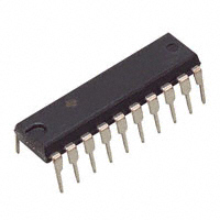
Pinout
CD54AC245, CD54ACT245
(CERDIP)
CD74AC245, CD74ACT245
(PDIP, SOIC, SSOP)
TOP VIEW
DIR
1
A0
2
19 OE
A1
3
18 B0
A2
4
17 B1
A3
5
16 B2
A4
6
15 B3
A5
7
14 B4
A6
8
13 B5
A7
9
12 B6
GND 10
11 B7
20 VCC
CAUTION: These devices are sensitive to electrostatic discharge. Users should follow proper IC Handling Procedures.
FAST™ is a Trademark of Fairchild Semiconductor.
Copyright © 2000, Texas Instruments Incorporated
1
�CD54/74AC245, CD54/74ACT245
Functional Diagram
A0
A1
A2
A3
A4
A5
A6
A7
2
18
3
17
4
16
5
15
6
14
7
13
8
12
9
11
B0
B1
B2
B3
B4
B5
B6
B7
1
DIR
19
OE
TRUTH TABLE
CONTROL INPUTS
OE
DIR
OPERATION
L
L
B Data to A Bus
L
H
A Data to B Bus
H
X
Isolation
H = High Level, L = Low Level, X = Irrelevant
To prevent excess currents in the High-Z (isolation) modes, all I/O
terminals should be terminated with 10kΩ to 1MΩ resistors.
2
�CD54/74AC245, CD54/74ACT245
Absolute Maximum Ratings
Thermal Information
DC Supply Voltage, VCC . . . . . . . . . . . . . . . . . . . . . . . . -0.5V to 6V
DC Input Diode Current, IIK
For VI < -0.5V or VI > VCC + 0.5V . . . . . . . . . . . . . . . . . . . . . .±20mA
DC Output Diode Current, IOK
For VO < -0.5V or VO > VCC + 0.5V . . . . . . . . . . . . . . . . . . . .±50mA
DC Output Source or Sink Current per Output Pin, IO
For VO > -0.5V or VO < VCC + 0.5V . . . . . . . . . . . . . . . . . . . .±50mA
DC VCC or Ground Current, ICC or IGND (Note 3) . . . . . . . . .±100mA
Thermal Resistance (Typical, Note 5)
θJA (oC/W)
E Package . . . . . . . . . . . . . . . . . . . . . . . . . . . . . . . .
69
M Package. . . . . . . . . . . . . . . . . . . . . . . . . . . . . . . .
58
SM Package . . . . . . . . . . . . . . . . . . . . . . . . . . . . . .
70
Maximum Junction Temperature (Plastic Package) . . . . . . . . . . 150oC
Maximum Storage Temperature Range . . . . . . . . . .-65oC to 150oC
Maximum Lead Temperature (Soldering 10s) . . . . . . . . . . . . . 300oC
Operating Conditions
Temperature Range, TA . . . . . . . . . . . . . . . . . . . . . . -55oC to 125oC
Supply Voltage Range, VCC (Note 4)
AC Types. . . . . . . . . . . . . . . . . . . . . . . . . . . . . . . . . . .1.5V to 5.5V
ACT Types . . . . . . . . . . . . . . . . . . . . . . . . . . . . . . . . .4.5V to 5.5V
DC Input or Output Voltage, VI, VO . . . . . . . . . . . . . . . . . 0V to VCC
Input Rise and Fall Slew Rate, dt/dv
AC Types, 1.5V to 3V . . . . . . . . . . . . . . . . . . . . . . . . . 50ns (Max)
AC Types, 3.6V to 5.5V . . . . . . . . . . . . . . . . . . . . . . . . 20ns (Max)
ACT Types, 4.5V to 5.5V. . . . . . . . . . . . . . . . . . . . . . . 10ns (Max)
CAUTION: Stresses above those listed in “Absolute Maximum Ratings” may cause permanent damage to the device. This is a stress only rating and operation
of the device at these or any other conditions above those indicated in the operational sections of this specification is not implied.
NOTES:
3. For up to 4 outputs per device, add ±25mA for each additional output.
4. Unless otherwise specified, all voltages are referenced to ground.
5. The package thermal impedance is calculated in accordance with JESD 51-7.
DC Electrical Specifications
TEST
CONDITIONS
PARAMETER
-40oC TO
85oC
25oC
-55oC TO
125oC
SYMBOL
VI (V)
IO (mA)
VCC
(V)
MIN
MAX
MIN
MAX
MIN
MAX
UNITS
VIH
-
-
1.5
1.2
-
1.2
-
1.2
-
V
3
2.1
-
2.1
-
2.1
-
V
5.5
3.85
-
3.85
-
3.85
-
V
1.5
-
0.3
-
0.3
-
0.3
V
3
-
0.9
-
0.9
-
0.9
V
5.5
-
1.65
-
1.65
-
1.65
V
1.5
1.4
-
1.4
-
1.4
-
V
AC TYPES
High Level Input Voltage
Low Level Input Voltage
High Level Output Voltage
VIL
VOH
-
VIH or VIL
-
-0.05
-0.05
3
2.9
-
2.9
-
2.9
-
V
-0.05
4.5
4.4
-
4.4
-
4.4
-
V
-4
3
2.58
-
2.48
-
2.4
-
V
-24
4.5
3.94
-
3.8
-
3.7
-
V
-75
(Note 6, 7)
5.5
-
-
3.85
-
-
-
V
-50
(Note 6, 7)
5.5
-
-
-
-
3.85
-
V
3
�CD54/74AC245, CD54/74ACT245
DC Electrical Specifications
(Continued)
TEST
CONDITIONS
PARAMETER
Low Level Output Voltage
-40oC TO
85oC
25oC
-55oC TO
125oC
SYMBOL
VI (V)
IO (mA)
VCC
(V)
MIN
MAX
MIN
MAX
MIN
MAX
UNITS
VOL
VIH or VIL
0.05
1.5
-
0.1
-
0.1
-
0.1
V
0.05
3
-
0.1
-
0.1
-
0.1
V
0.05
4.5
-
0.1
-
0.1
-
0.1
V
12
3
-
0.36
-
0.44
-
0.5
V
24
4.5
-
0.36
-
0.44
-
0.5
V
75
(Note 6, 7)
5.5
-
-
-
1.65
-
-
V
50
(Note 6, 7)
5.5
-
-
-
-
-
1.65
V
Input Leakage Current
II
VCC or
GND
-
5.5
-
±0.1
-
±1
-
±1
µA
Three-State Leakage
Current
IOZ
VIH or VIL
VO = VCC
or GND
-
5.5
-
±0.5
-
±5
-
±10
µA
Quiescent Supply Current
MSI
ICC
VCC or
GND
0
5.5
-
8
-
80
-
160
µA
High Level Input Voltage
VIH
-
-
4.5 to
5.5
2
-
2
-
2
-
V
Low Level Input Voltage
VIL
-
-
4.5 to
5.5
-
0.8
-
0.8
-
0.8
V
High Level Output Voltage
VOH
VIH or VIL
-0.05
4.5
4.4
-
4.4
-
4.4
-
V
-24
4.5
3.94
-
3.8
-
3.7
-
V
-75
(Note 6, 7)
5.5
-
-
3.85
-
-
-
V
-50
(Note 6, 7)
5.5
-
-
-
-
3.85
-
V
0.05
4.5
-
0.1
-
0.1
-
0.1
V
24
4.5
-
0.36
-
0.44
-
0.5
V
75
(Note 6, 7)
5.5
-
-
-
1.65
-
-
V
50
(Note 6, 7)
5.5
-
-
-
-
-
1.65
V
ACT TYPES
Low Level Output Voltage
VOL
VIH or VIL
II
VCC or
GND
-
5.5
-
±0.1
-
±1
-
±1
µA
Three-State or Leakage
Current
IOZ
VIH or VIL
VO = VCC
or GND
-
5.5
-
±0.5
-
±5
-
±10
µA
Quiescent Supply Current
MSI
ICC
VCC or
GND
0
5.5
-
8
-
80
-
160
µA
∆ICC
VCC
-2.1
-
4.5 to
5.5
-
2.4
-
2.8
-
3
mA
Input Leakage Current
Additional Supply Current per
Input Pin TTL Inputs High
1 Unit Load
NOTES:
6. Test one output at a time for a 1-second maximum duration. Measurement is made by forcing current and measuring voltage to minimize
power dissipation.
7. Test verifies a minimum 50Ω transmission-line-drive capability at 85oC, 75Ω at 125oC.
4
�CD54/74AC245, CD54/74ACT245
ACT Input Load Table
INPUT
UNIT LOAD
An, Bn
0.83
OE
0.64
DIR
0.25
NOTE: Unit load is ∆ICC limit specified in DC Electrical Specifications
Table, e.g., 2.4mA max at 25oC.
Switching Specifications Input tr, tf = 3ns, CL = 50pF (Worst Case)
-40oC TO 85oC
PARAMETER
-55oC TO 125oC
SYMBOL
VCC (V)
MIN
TYP
MAX
MIN
TYP
MAX
UNITS
tPLH, tPHL
1.5
-
-
96
-
-
106
ns
3.3
(Note 9)
3.2
-
10.8
3
-
11.9
ns
5
(Note 10)
2.2
-
7.7
2.1
-
8.5
ns
1.5
-
-
159
-
-
175
ns
3.3
4.7
-
15.9
4.4
-
17.5
ns
5
3.7
-
12.7
3.5
-
14
ns
1.5
-
-
159
-
-
175
ns
3.3
5.6
-
19
5.3
-
21
ns
5
3.7
-
12.7
3.5
-
14
ns
AC TYPES
Propagation Delay,
Data to Output
Propagation Delay,
Output Disable to Output
Propagation Delay,
Output Enable to Output
tPLZ, tPHZ
tPZL, tPZH
Minimum (Valley) VOH During
Switching of Other Outputs
(Output Under Test Not Switching)
VOHV
See Figure 1
5
-
4 at
25oC
-
-
4 at
25oC
-
V
Maximum (Peak) VOL During
Switching of Other Outputs
(Output Under Test Not Switching)
VOLP
See Figure 1
5
-
1 at
25oC
-
-
1 at
25oC
-
V
Three-State Output Capacitance
CO
-
-
15
-
-
15
-
pF
Input Capacitance
CI
-
-
-
10
-
-
10
pF
CPD
(Note 11)
-
-
57
-
-
57
-
pF
Propagation Delay,
Data to Output
tPLH, tPHL
5
(Note 10)
2.7
-
9.1
2.5
-
10
ns
Propagation Delay,
Output Disable to Output
tPLZ, tPHZ
5
3.7
12.7
3.5
14
ns
Propagation Delay,
Output Enable to Output
tPZL, tPZH
5
3.8
13.1
3.6
14.4
ns
Minimum (Valley) VOH During
Switching of Other Outputs
(Output Under Test Not Switching)
VOHV
See Figure 1
5
-
4 at
25oC
-
-
4 at
25oC
-
V
Maximum (Peak) VOL During
Switching of Other Outputs
(Output Under Test Not Switching)
VOLP
See Figure 1
5
-
1 at
25oC
-
-
1 at
25oC
-
V
Power Dissipation Capacitance
ACT TYPES
5
�CD54/74AC245, CD54/74ACT245
Switching Specifications Input tr, tf = 3ns, CL = 50pF (Worst Case)
(Continued)
-40oC TO 85oC
-55oC TO 125oC
SYMBOL
VCC (V)
MIN
TYP
MAX
MIN
TYP
MAX
UNITS
Three-State Output Capacitance
CO
-
-
15
-
-
15
-
pF
Input Capacitance
CI
-
-
-
10
-
-
10
pF
CPD
(Note 11)
-
-
57
-
-
57
-
pF
PARAMETER
Power Dissipation Capacitance
NOTES:
8. Limits tested 100%
9. 3.3V Min is at 3.6V, Max is at 3V.
10. 5V Min is at 5.5V, Max is at 4.5V.
11. CPD is used to determine the dynamic power consumption per channel.
AC: PD = VCC2 fi (CPD + CL)
ACT: PD = VCC2 fi (CPD + CL) + VCC ∆ICC where fi = input frequency, CL = output load capacitance, VCC = supply voltage.
VOH
OTHER
OUTPUTS
VOL
VOH
VOHV
OUTPUT
UNDER
TEST
VOLP
VOL
NOTES:
12. Input pulses have the following characteristics: PRR ≤ 1MHz, tr = 3ns, SKEW 1ns.
13. R.F. fixture with 700MHz design rules required. IC should be soldered into test board and bypassed with 0.1µF capacitor. Scope and
probes require 700MHz bandwidth.
FIGURE 1. SIMULTANEOUS SWITCHING TRANSIENT WAVEFORMS
6
�CD54/74AC245, CD54/74ACT245
tf = 3ns
tr = 3ns
INPUT LEVEL
90%
OUTPUTS
DISABLED
VS
10%
tPLZ
GND
tPZL
OUTPUT:
LOW TO OFF
TO LOW
VS
0.2 VCC
tPHZ
VOL (≠ VCC)
tPZH
0.8 VCC
VS
OUTPUT:
HIGH TO OFF
TO HIGH
OUTPUTS
ENABLED
OUTPUTS
DISABLED
OUTPUTS
ENABLED
GND (tPHZ, tPZH)
OTHER
INPUTS
TIED HIGH
OR LOW
OUTPUT
DISABLE
OPEN (tPHL, tPLH)
2 VCC (tPLZ, tPZL)
RL
500Ω (OPEN DRAIN)
OUT
RL
CL
500Ω
50pF
(NOTE 14)
DUT WITH
THREESTATE
OUTPUT
NOTE:
14. For AC Series only: When VCC = 1.5V, RL = 1kΩ.
FIGURE 2. THREE-STATE PROPAGATION DELAY TIMES AND TEST CIRCUIT
tr = 3ns
tf = 3ns
INPUT
LEVEL
90%
VS
10%
An
GND
tPHL
tPLH
VS
Bn
FIGURE 3. PROPAGATION DELAY TIMES
OUTPUT
RL (NOTE)
500Ω
DUT
OUTPUT
LOAD
CL
50pF
NOTE: For AC Series Only: When VCC = 1.5V, RL = 1kΩ.
AC
ACT
VCC
3V
Input Switching Voltage, VS
0.5 VCC
1.5V
Output Switching Voltage, VS
0.5 VCC
0.5 VCC
Input Level
FIGURE 4. PROPAGATION DELAY TIMES
7
�PACKAGE OPTION ADDENDUM
www.ti.com
14-Oct-2022
PACKAGING INFORMATION
Orderable Device
Status
(1)
Package Type Package Pins Package
Drawing
Qty
Eco Plan
(2)
Lead finish/
Ball material
MSL Peak Temp
Op Temp (°C)
Device Marking
(3)
Samples
(4/5)
(6)
CD54AC245F3A
ACTIVE
CDIP
J
20
1
Non-RoHS
& Green
SNPB
N / A for Pkg Type
-55 to 125
CD54AC245F3A
Samples
CD54ACT245F3A
ACTIVE
CDIP
J
20
1
Non-RoHS
& Green
SNPB
N / A for Pkg Type
-55 to 125
CD54ACT245F3A
Samples
CD74AC245E
ACTIVE
PDIP
N
20
20
RoHS & Green
NIPDAU
N / A for Pkg Type
-55 to 125
CD74AC245E
Samples
CD74AC245EE4
ACTIVE
PDIP
N
20
20
RoHS & Green
NIPDAU
N / A for Pkg Type
-55 to 125
CD74AC245E
Samples
CD74AC245M
ACTIVE
SOIC
DW
20
25
RoHS & Green
NIPDAU
Level-1-260C-UNLIM
-55 to 125
AC245M
Samples
CD74AC245M96
ACTIVE
SOIC
DW
20
2000
RoHS & Green
NIPDAU
Level-1-260C-UNLIM
-55 to 125
AC245M
Samples
CD74ACT245E
ACTIVE
PDIP
N
20
20
RoHS & Green
NIPDAU
N / A for Pkg Type
-55 to 125
CD74ACT245E
Samples
CD74ACT245EE4
ACTIVE
PDIP
N
20
20
RoHS & Green
NIPDAU
N / A for Pkg Type
-55 to 125
CD74ACT245E
Samples
CD74ACT245M
ACTIVE
SOIC
DW
20
25
RoHS & Green
NIPDAU
Level-1-260C-UNLIM
-55 to 125
ACT245M
Samples
CD74ACT245M96
ACTIVE
SOIC
DW
20
2000
RoHS & Green
NIPDAU
Level-1-260C-UNLIM
-55 to 125
ACT245M
Samples
CD74ACT245MG4
ACTIVE
SOIC
DW
20
25
RoHS & Green
NIPDAU
Level-1-260C-UNLIM
-55 to 125
ACT245M
Samples
CD74ACT245SM96
ACTIVE
SSOP
DB
20
2000
RoHS & Green
NIPDAU
Level-1-260C-UNLIM
-55 to 125
ACT245SM
Samples
(1)
The marketing status values are defined as follows:
ACTIVE: Product device recommended for new designs.
LIFEBUY: TI has announced that the device will be discontinued, and a lifetime-buy period is in effect.
NRND: Not recommended for new designs. Device is in production to support existing customers, but TI does not recommend using this part in a new design.
PREVIEW: Device has been announced but is not in production. Samples may or may not be available.
OBSOLETE: TI has discontinued the production of the device.
(2)
RoHS: TI defines "RoHS" to mean semiconductor products that are compliant with the current EU RoHS requirements for all 10 RoHS substances, including the requirement that RoHS substance
do not exceed 0.1% by weight in homogeneous materials. Where designed to be soldered at high temperatures, "RoHS" products are suitable for use in specified lead-free processes. TI may
reference these types of products as "Pb-Free".
RoHS Exempt: TI defines "RoHS Exempt" to mean products that contain lead but are compliant with EU RoHS pursuant to a specific EU RoHS exemption.
Green: TI defines "Green" to mean the content of Chlorine (Cl) and Bromine (Br) based flame retardants meet JS709B low halogen requirements of