CD74HC4538-Q1
HIGH-SPEED CMOS LOGIC DUAL RETRIGGERABLE
PRECISION MONOSTABLE MULTIVIBRATOR
SCLS595A − NOVEMBER 2004 − REVISED APRIL 2008
D Qualified for Automotive Applications
D Retriggerable/Resettable Capability
D Trigger and Reset Propagation Delays
D
D
D
D
D
D
D
Independent of RX, CX
Triggering From the Leading or Trailing
Edge
Q and Q Buffered Outputs Available
Separate Resets
Wide Range of Output Pulse Widths
Schmitt-Trigger Input on A and B Inputs
Retrigger Time Is Independent of CX
Fanout (Over Temperature Range)
− Standard Outputs . . . 10 LSTTL Loads
− Bus Driver Outputs . . . 15 LSTTL Loads
D Balanced Propagation Delay and Transition
Times
D Significant Power Reduction Compared to
D
D
LSTTL Logic ICs
VCC Voltage = 2 V to 6 V
High Noise Immunity NIL or NIH = 30% of
VCC, VCC = 5 V
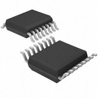
M OR PW PACKAGE
(TOP VIEW)
1CX
1RXCX
1R
1A
1B
1Q
1Q
GND
description/ordering information
1
16
2
15
3
14
4
13
5
12
6
11
7
10
VCC
2CX
2RXCX
2R
2A
2B
2Q
2Q
8
9
The CD74HC4538 is a dual retriggerable/resettable
precision monostable multivibrator for fixed-voltage
timing applications. An external resistor (RX) and
external capacitor (CX) control the timing and accuracy for the circuit. Adjustment of RX and CX provides a wide
range of output pulse widths from the Q and Q terminals. The propagation delay from trigger input-to-output
transition and the propagation delay from reset input-to-output transition are independent of RX and CX.
Leading-edge triggering (A) and trailing-edge triggering (B) inputs are provided for triggering from either edge
of the input pulse. An unused A input should be tied to GND and an unused B input should be tied to VCC. On
power up, the IC is reset. Unused resets and sections must be terminated. In normal operation, the circuit
retriggers on the application of each new trigger pulse. To operate in the nontriggerable mode, Q is connected
to B when leading-edge triggering (A) is used, or Q is connected to A when trailing-edge triggering (B) is used.
The period (τ) can be calculated from τ = (0.7) RX, CX; RMIN is 5 kΩ. CMIN is 0 pF.
ORDERING INFORMATION{
PACKAGE‡
TA
−40°C
40°C to 125°C
ORDERABLE
PART NUMBER
TOP-SIDE
MARKING
SOIC − M
Tape and reel
CD74HC4538QM96Q1
HC4538M
TSSOP − PW
Tape and reel
CD74HC4538QPWRQ1
HC4538M
†
For the most current package and ordering information, see the Package Option Addendum at the
end of this document, or see the TI web site at http://www.ti.com.
‡ Package drawings, thermal data, and symbolization are available at http://www.ti.com/packaging.
Please be aware that an important notice concerning availability, standard warranty, and use in critical applications of
Texas Instruments semiconductor products and disclaimers thereto appears at the end of this data sheet.
Copyright 2008, Texas Instruments Incorporated
PRODUCTION DATA information is current as of publication date.
Products conform to specifications per the terms of Texas Instruments
standard warranty. Production processing does not necessarily include
testing of all parameters.
POST OFFICE BOX 655303
• DALLAS, TEXAS 75265
1
�CD74HC4538-Q1
HIGH-SPEED CMOS LOGIC DUAL RETRIGGERABLE
PRECISION MONOSTABLE MULTIVIBRATOR
SCLS595A − NOVEMBER 2004 − REVISED APRIL 2008
FUNCTION TABLE
OUTPUTS
INPUTS
R
A
B
Q
Q
L
X
X
L
H
X
H
X
L
H
X
X
L
L
H
H
L
↓
H
↑
H
NOTE: H = High voltage level
L = Low voltage level
↑ = Transition from low to high level
↓ = Transition from high to low level
= one high-level pulse
= one low-level pulse
X = Irrelevant
logic diagram (positive logic)
16
VCC
VCC
VCC
VCC
RX
2(14)
CX
R1
+
Comp II
6(10)
Q
−
1(15)
R2
VCC
VCC
8
7(9)
Q
High Z
3(13)
VCC
4(12)
D R1
5(11)
2
CL
R2
FF
CL
Q
Q
POST OFFICE BOX 655303
• DALLAS, TEXAS 75265
�CD74HC4538-Q1
HIGH-SPEED CMOS LOGIC DUAL RETRIGGERABLE
PRECISION MONOSTABLE MULTIVIBRATOR
SCLS595A − NOVEMBER 2004 − REVISED APRIL 2008
FUNCTIONAL TERMINAL CONNECTIONS
VCC TO
TERMINAL NUMBER
GND TO
TERMINAL NUMBER
INPUT PULSE TO
TERMINAL NUMBER
MONO1
MONO2
MONO1
MONO1
MONO2
3, 5
11, 13
4
12
Leading-edge
trigger/nonretriggerable
3
13
4
12
Trailing-edge
trigger/retriggerable
3
13
5
11
Trailing-edge
trigger/nonretriggerable
3
13
5
11
FUNCTION
Leading-edge
trigger/retriggerable
MONO2
4
12
OTHER CONNECTIONS
MONO1
MONO2
5−7
11−9
4−6
12−10
NOTES: 1. A retriggerable one-shot multivibrator has an output pulse width that is extended one full time period (T) after application of the last
trigger pulse.
2. A nontriggerable one-shot multivibrator has a time period (T) referenced from the application of the first trigger pulse.
T
Input Pulse Train
Retriggerable Mode
Pulse Width (A Mode)
T
Nonretriggerable Mode
Pulse Width (A Mode)
absolute maximum ratings over operating free-air temperature range (unless otherwise noted)†
Supply voltage range, VCC (see Note 1) . . . . . . . . . . . . . . . . . . . . . . . . . . . . . . . . . . . . . . . . . . . . . . −0.5 V to 7 V
Input clamp current, IIK (VI < −0.5 V or VI > VCC + 0.5 V) . . . . . . . . . . . . . . . . . . . . . . . . . . . . . . . . . . . . . ±20 mA
Output clamp current, IOK (VO < −0.5 V or VO > VCC + 0.5 V) . . . . . . . . . . . . . . . . . . . . . . . . . . . . . . . . . ±20 mA
Switch current per output pin, IO (VO > −0.5 V or VO < VCC + 0.5 V) . . . . . . . . . . . . . . . . . . . . . . . . . . . ±25 mA
Continuous current through VCC or GND . . . . . . . . . . . . . . . . . . . . . . . . . . . . . . . . . . . . . . . . . . . . . . . . . . . ±50 mA
Package thermal impedance, θJA (see Note 2): M package . . . . . . . . . . . . . . . . . . . . . . . . . . . . . . . . . . 73°C/W
PW package . . . . . . . . . . . . . . . . . . . . . . . . . . . . . . . . 108°C/W
Maximum junction temperature, TJ . . . . . . . . . . . . . . . . . . . . . . . . . . . . . . . . . . . . . . . . . . . . . . . . . . . . . . . . . 150°C
Lead temperature (during soldering):
At distance 1/16 ± 1/32 inch (1,59 ± 0,79 mm) from case for 10 s max . . . . . . . . . . . . . . . . . . . . . . . 300°C
Storage temperature range, Tstg . . . . . . . . . . . . . . . . . . . . . . . . . . . . . . . . . . . . . . . . . . . . . . . . . . . −65°C to 150°C
†
Stresses beyond those listed under “absolute maximum ratings” may cause permanent damage to the device. These are stress ratings only, and
functional operation of the device at these or any other conditions beyond those indicated under “recommended operating conditions” is not
implied. Exposure to absolute-maximum-rated conditions for extended periods may affect device reliability.
NOTES: 1. All voltages are referenced to GND, unless otherwise specified.
2. The package thermal impedance is calculated in accordance with JESD 51-7.
POST OFFICE BOX 655303
• DALLAS, TEXAS 75265
3
�CD74HC4538-Q1
HIGH-SPEED CMOS LOGIC DUAL RETRIGGERABLE
PRECISION MONOSTABLE MULTIVIBRATOR
SCLS595A − NOVEMBER 2004 − REVISED APRIL 2008
recommended operating conditions (see Note 3)
VCC
Supply voltage
VIH
High-level
High
level input voltage
VCC = 2 V
VCC = 4.5 V
VCC = 6 V
MIN
MAX
2
6
UNIT
V
1.5
3.15
V
4.2
VCC = 2 V
0.5
VCC = 4.5 V
1.35
VIL
Low-level
Low level input voltage
VI
Input voltage
0
VCC
V
VO
Output voltage
0
VCC
V
VCC = 2 V
0
1000
VCC = 4.5 V
0
500
VCC = 6 V
0
400
VCC = 2 V
0
Unlimited
VCC = 4.5 V
0
Unlimited
VCC = 6 V
0
Unlimited
VCC = 6 V
Reset input
tt
Input transition (rise and fall) time
Trigger inputs A or B
V
1.8
ns
RX
External timing resistor (see Note 4)
5
kΩ
CX
External timing capacitor (see Note 4)
0
F
TA
Operating free-air temperature
−40
125
°C
NOTES: 3. All unused inputs of the device must be held at VCC or GND to ensure proper device operation. Refer to the TI application report,
Implications of Slow or Floating CMOS Inputs, literature number SCBA004.
4. The maximum allowable values of RX and CX are a function of leakage of capacitor CX, leakage of the CD74HC4538, and leakage
due to board layout and surface resistance. Values of RX and CX should be chosen so that the maximum current into pin 2 or
pin 14 is 30 mA. Susceptibility to externally induced noise signals may occur for RX > 1 MΩ.
4
POST OFFICE BOX 655303
• DALLAS, TEXAS 75265
�CD74HC4538-Q1
HIGH-SPEED CMOS LOGIC DUAL RETRIGGERABLE
PRECISION MONOSTABLE MULTIVIBRATOR
SCLS595A − NOVEMBER 2004 − REVISED APRIL 2008
electrical characteristics over recommended operating free-air temperature range (unless
otherwise noted)
PARAMETER
TEST CONDITIONS
CMOS loads
VOH
CMOS loads
II
VI = VCC or GND
ICC
VI = VCC or GND
CIN
CL = 50 pF
TA = 25°C
TA = −40°C
TO 85°C
TA = −40°C
TO 125°C
MIN
MIN
MIN
MAX
MAX
1.9
1.9
1.9
4.5 V
4.4
4.4
4.4
6V
5.9
5.9
5.9
−4
4.5 V
3.98
3.84
3.7
−5.2
6V
5.48
−0.02
0.02
5.34
UNIT
MAX
V
5.2
2V
0.1
0.1
0.1
0.02
4.5 V
0.1
0.1
0.1
6V
0.1
0.1
0.1
4
4.5 V
0.26
0.33
0.4
5.2
6V
0.26
0.33
0.4
VI = VIH or VIL
TTL loads
VCC
2V
VI = VIH or VIL
TTL loads
VOL
IO
(mA)
A, B, R
6V
±0.1
±1
±1
RXCX (see Note 5)
6V
±0.05
±0.5
±0.5
V
A
µA
Quiescent
0
6V
8
80
160
µA
Active, Q = high,
Pins 2 and 14 at VCC/4
0
6V
0.6
0.8
1
mA
10
10
10
pF
NOTE 5: When testing IIL, the Q output must be high. If Q is low (device not triggered), the pullup P device is ON and the low-resistance path
from VDD to the test pin causes a current far exceeding the specification.
timing requirements over recommended operating free-air temperature range (unless otherwise
noted) (see Figure 1)
PARAMETER
TA = 25°C
VCC
MIN
tw
tsu
trr
Input pulse width
Reset setup time
Retrigger time (see Figure 4)
TYP
MAX
TA = −40°C
TO 85°C
TA = −40°C
TO 125°C
MIN
MIN
MAX
2V
80
100
120
4.5 V
16
20
24
6V
14
17
20
2V
5
5
5
4.5 V
5
5
5
6V
5
5
5
5V
Output pulse-width match, same package
POST OFFICE BOX 655303
UNIT
MAX
ns
ns
175
ns
±1
%
• DALLAS, TEXAS 75265
5
�CD74HC4538-Q1
HIGH-SPEED CMOS LOGIC DUAL RETRIGGERABLE
PRECISION MONOSTABLE MULTIVIBRATOR
SCLS595A − NOVEMBER 2004 − REVISED APRIL 2008
switching characteristics over recommended operating free-air temperature range (unless
otherwise noted) (see Figure 1)
PARAMETER
FROM
(INPUT)
A B
A,
TO
(OUTPUT)
Q or Q
LOAD
CAPACITANCE
CL = 50 pF
CL = 15 pF
tpd
R
Q or Q
CL = 50 pF
CL = 15 pF
tt
τ†
†
CL = 50 pF
CL = 50 pF
TA = 25°C
VCC
MIN
TYP
MAX
TA = −40°C
TO 85°C
TA = −40°C
TO 125°C
MIN
MIN
MAX
2V
250
315
375
4.5 V
50
63
75
6V
43
54
64
2V
250
315
375
4.5 V
50
63
75
6V
43
54
64
2V
75
95
110
4.5 V
15
19
22
6V
13
16
19
5V
UNIT
MAX
21
5V
ns
21
3V
0.64
0.78
0.612
0.812
0.605
0.819
5V
0.63
0.77
0.602
0.798
0.595
0.805
ns
ms
Output pulse width with RX = 10 kΩ and CX = 0.1 µF
operating characteristics, VCC = 5 V, TA = 25°C, input tr, tf = 6 ns, CL = 15 pF
PARAMETER
Cpd
Power dissipation capacitance (see Note 6)
NOTE 6: Cpd is used to determine the dynamic power consumption, per one shot.
PD = (Cpd + CX) VCC2 fI Σ(CL VCC2 fO)
fI = input frequency
fO = output frequency
CL = output load capacitance
CX = external capacitance
VCC = supply voltage, assuming fI % l/τ
6
POST OFFICE BOX 655303
• DALLAS, TEXAS 75265
TYP
UNIT
136
pF
�CD74HC4538-Q1
HIGH-SPEED CMOS LOGIC DUAL RETRIGGERABLE
PRECISION MONOSTABLE MULTIVIBRATOR
SCLS595A − NOVEMBER 2004 − REVISED APRIL 2008
PARAMETER MEASUREMENT INFORMATION
From Output
Under Test
VCC
High-Level
Pulse
Test
Point
50%
50%
0V
tw
CL = 50 pF
(see Note A)
VCC
Low-Level
Pulse
50%
50%
0V
LOAD CIRCUIT
VOLTAGE WAVEFORMS
PULSE DURATIONS
VCC
Input
50%
50%
0V
tPLH
VCC
Reference
Input
In-Phase
Output
50%
50%
10%
0V
tsu
Data
Input
50%
10%
90%
tr
tPHL
VCC
50%
10% 0 V
90%
90%
tr
th
90%
tPHL
Out-of-Phase
Output
90%
VOLTAGE WAVEFORMS
SETUP AND HOLD AND INPUT RISE AND FALL TIMES
tPLH
50%
10%
tf
tf
VOH
50%
10%
VOL
tf
50%
10%
90%
VOH
VOL
tr
VOLTAGE WAVEFORMS
PROPAGATION DELAY AND OUTPUT TRANSITION TIMES
NOTES: A. CL includes probe and test-fixture capacitance.
B. Phase relationships between waveforms were chosen arbitrarily. All input pulses are supplied by generators having the following
characteristics: PRR ≤ 1 MHz, ZO = 50 Ω, tr = 6 ns, tf = 6 ns.
C. For clock inputs, fmax is measured when the input duty cycle is 50%.
D. The outputs are measured one at a time, with one input transition per measurement.
E. tPLH and tPHL are the same as tpd.
Figure 1. Load Circuit and Voltage Waveforms
POST OFFICE BOX 655303
• DALLAS, TEXAS 75265
7
�CD74HC4538-Q1
HIGH-SPEED CMOS LOGIC DUAL RETRIGGERABLE
PRECISION MONOSTABLE MULTIVIBRATOR
SCLS595A − NOVEMBER 2004 − REVISED APRIL 2008
TYPICAL CHARACTERISTICS
HC4538
TA = 25°C
0.7
K Factor
10 kΩ, 10 nF
0.69
10 kΩ ,100 nF
100 kΩ, 100 nF
0.68
100 kΩ, 10 nF
0.67
2
3
4
4.5
5
5.5
6
VCC − DC Supply Voltage − V
Figure 2. K Factor vs DC Supply Voltage
1.3
1.2
K Factor
1.1
1
0.9
0.8
2 kΩ
0.7
10 kΩ
100 kΩ
0.6
10
102
103
104
105
t rr , TYP MIN Retrigger Time − ns
104
HC4538
VCC = 5 V
TA = 25°C
TA = 25°C
RX = 10 kΩ
103
VCC = 4.5 V
102
VCC = 5 V
10
CX − Timing Capacitance − pF
Figure 3. K Factor vs CX
8
POST OFFICE BOX 655303
102
103
CX − Timing Capacitance − pF
Figure 4. Minimum Retrigger Time
vs Timing Capacitance
• DALLAS, TEXAS 75265
104
�CD74HC4538-Q1
HIGH-SPEED CMOS LOGIC DUAL RETRIGGERABLE
PRECISION MONOSTABLE MULTIVIBRATOR
SCLS595A − NOVEMBER 2004 − REVISED APRIL 2008
TYPICAL APPLICATION DATA
power-down mode
During a rapid power-down condition (as would occur with a power-supply short circuit with a poorly filtered
power supply), the energy stored in CX could discharge into pin 2 or pin 14. To avoid possible device damage
in this mode when CX is w 0.5 µF, a protection diode with a 1-A rating or higher (1N5395 or equivalent) and a
separate ground return for CX should be provided (see Figure 5).
An alternate protection method is shown in Figure 6, where a 51-Ω current-limiting resistor is inserted in series
with CX . Note that a small pulse-duration decrease occurs, however, and RX must be increased appropriately
to obtain the originally desired pulse duration.
VCC
VCC
RX
RX
2 (14)
16
2 (14)
16
1 (15)
8
51 Ω
CX
≥0.5 µF
1 (15)
CX
≥0.5 µF
8
Figure 5. Rapid-Power-Down
Protection Circuit
POST OFFICE BOX 655303
Figure 6. Alternative Rapid-Power-Down
Protection Circuit
• DALLAS, TEXAS 75265
9
�PACKAGE OPTION ADDENDUM
www.ti.com
10-Dec-2020
PACKAGING INFORMATION
Orderable Device
Status
(1)
Package Type Package Pins Package
Drawing
Qty
Eco Plan
(2)
Lead finish/
Ball material
MSL Peak Temp
Op Temp (°C)
Device Marking
(3)
(4/5)
(6)
CD74HC4538QM96G4Q1
ACTIVE
SOIC
D
16
2500
RoHS & Green
NIPDAU
Level-1-260C-UNLIM
-40 to 125
HC4538M
CD74HC4538QPWRG4Q1
ACTIVE
TSSOP
PW
16
2000
RoHS & Green
NIPDAU
Level-1-260C-UNLIM
-40 to 125
HC4538M
CD74HC4538QPWRQ1
ACTIVE
TSSOP
PW
16
2000
RoHS & Green
NIPDAU
Level-1-260C-UNLIM
-40 to 125
HC4538M
(1)
The marketing status values are defined as follows:
ACTIVE: Product device recommended for new designs.
LIFEBUY: TI has announced that the device will be discontinued, and a lifetime-buy period is in effect.
NRND: Not recommended for new designs. Device is in production to support existing customers, but TI does not recommend using this part in a new design.
PREVIEW: Device has been announced but is not in production. Samples may or may not be available.
OBSOLETE: TI has discontinued the production of the device.
(2)
RoHS: TI defines "RoHS" to mean semiconductor products that are compliant with the current EU RoHS requirements for all 10 RoHS substances, including the requirement that RoHS substance
do not exceed 0.1% by weight in homogeneous materials. Where designed to be soldered at high temperatures, "RoHS" products are suitable for use in specified lead-free processes. TI may
reference these types of products as "Pb-Free".
RoHS Exempt: TI defines "RoHS Exempt" to mean products that contain lead but are compliant with EU RoHS pursuant to a specific EU RoHS exemption.
Green: TI defines "Green" to mean the content of Chlorine (Cl) and Bromine (Br) based flame retardants meet JS709B low halogen requirements of