��������
���
��
�� ���� ���� ����� ���
��
�
SCAS621A − DECEMBER 1998 − REVISED DECEMBER 2004
D Use CDCVF2510A as a Replacement for
D
D
D
D
D
D
D
D
D
D
D
D
D
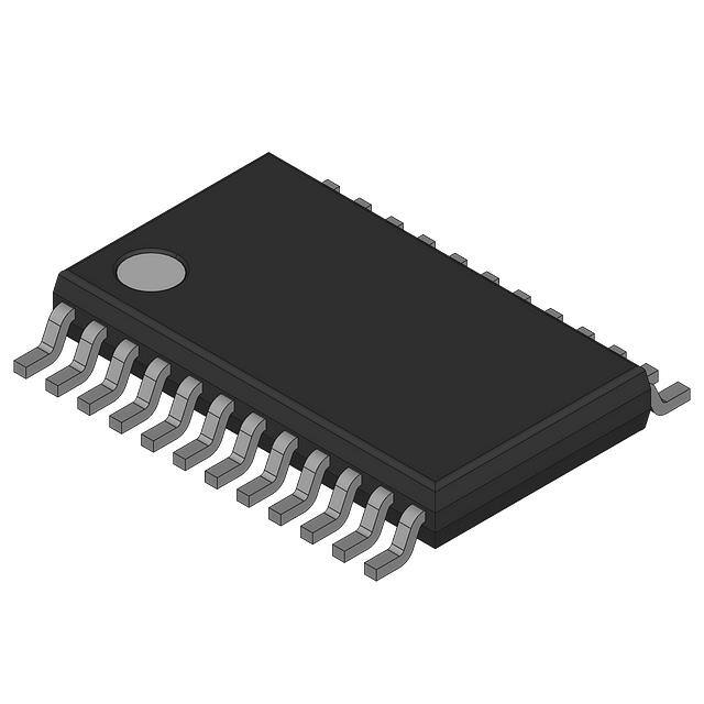
PW PACKAGE
(TOP VIEW)
this Device
Designed to Meet PC SDRAM Registered
DIMM Design Support Document Rev. 1.2
Spread Spectrum Clock Compatible
Operating Frequency 25 MHz to 125 MHz
Static tPhase Error Distribution at 66 MHz
to 100 MHz is ±150 ps
Drop-In Replacement for TI CDC2510A With
Enhanced Performance
Jitter (cyc − cyc) at 66 MHz to 100 MHz is
|100 ps|
Available in Plastic 24-Pin TSSOP
Phase-Lock Loop Clock Distribution for
Synchronous DRAM Applications
Distributes One Clock Input to One Bank of
Ten Outputs
External Feedback (FBIN) Terminal Is Used
to Synchronize the Outputs to the Clock
Input
On-Chip Series Damping Resistors
No External RC Network Required
Operates at 3.3 V
AGND
VCC
1Y0
1Y1
1Y2
GND
GND
1Y3
1Y4
VCC
G
FBOUT
1
24
2
23
3
22
4
21
5
20
6
19
7
18
8
17
9
16
10
15
11
14
12
13
CLK
AVCC
VCC
1Y9
1Y8
GND
GND
1Y7
1Y6
1Y5
VCC
FBIN
description
The CDC2510C is a high-performance, low-skew, low-jitter, phase-lock loop (PLL) clock driver. It uses a PLL
to precisely align, in both frequency and phase, the feedback (FBOUT) output to the clock (CLK) input signal.
It is specifically designed for use with synchronous DRAMs. The CDC2510C operates at VCC = 3.3 V . It also
provides integrated series-damping resistors that make it ideal for driving point-to-point loads.
One bank of ten outputs provides ten low-skew, low-jitter copies of CLK. Output signal duty cycles are adjusted
to 50 percent, independent of the duty cycle at CLK. All outputs can be enabled or disabled via a single output
enable input. When the G input is high, the outputs switch in phase and frequency with CLK; when the G input
is low, the outputs are disabled to the logic-low state.
Unlike many products containing PLLs, the CDC2510C does not require external RC networks. The loop filter
for the PLL is included on-chip, minimizing component count, board space, and cost.
Because it is based on PLL circuitry, the CDC2510C requires a stabilization time to achieve phase lock of the
feedback signal to the reference signal. This stabilization time is required, following power up and application
of a fixed-frequency, fixed-phase signal at CLK, and following any changes to the PLL reference or feedback
signals. The PLL can be bypassed for test purposes by strapping AVCC to ground.
The CDC2510C is characterized for operation from 0°C to 85°C.
For application information, see the High Speed Distribution Design Techniques for
CDC509/516/2509/2510/2516 (literature number SLMA003) and Using CDC2509A/2510A PLL with Spread
Spectrum Clocking (SSC) (literature number SCAA039) application reports.
Please be aware that an important notice concerning availability, standard warranty, and use in critical applications of
Texas Instruments semiconductor products and disclaimers thereto appears at the end of this data sheet.
Copyright 2004, Texas Instruments Incorporated
���������� �
�
�������!��� �" #$��%�! �" �� &$'(�#�!��� )�!%�
���)$#!" #������ !� "&%#���#�!���" &%� !*% !%��" �� �%+�" ��"!�$�%�!"
"!��)��) ,�����!-� ���)$#!��� &��#%""��. )�%" ��! �%#%""���(- ��#($)%
!%"!��. �� �(( &����%!%�"�
POST OFFICE BOX 655303
• DALLAS, TEXAS 75265
1
���������
���
��
�� ���� ���� ����� ���
��
�
SCAS621A − DECEMBER 1998 − REVISED DECEMBER 2004
FUNCTION TABLE
OUTPUTS
INPUTS
G
CLK
1Y
(0:9)
X
L
L
L
L
H
L
H
H
H
H
H
FBOUT
functional block diagram
G
11
3
4
5
8
9
15
16
CLK
24
ÎÎÎÎÎÎÎ
ÎÎÎÎÎÎÎ
ÁÁÁÁÁÁ
ÎÎÎÎÎÎÎ
ÁÁÁÁÁÁ
ÎÎÎÎÎÎÎ
17
PLL
FBIN
AVCC
13
20
21
1Y1
1Y2
1Y3
1Y4
1Y5
1Y6
1Y7
1Y8
1Y9
23
12
AVAILABLE OPTIONS
PACKAGE
2
1Y0
TA
SMALL OUTLINE
(PW)
0°C to 85°C
CDC2510CPWR
POST OFFICE BOX 655303
• DALLAS, TEXAS 75265
FBOUT
���������
���
��
�� ���� ���� ����� ���
��
�
SCAS621A − DECEMBER 1998 − REVISED DECEMBER 2004
Terminal Functions
TERMINAL
NAME
NO.
TYPE
DESCRIPTION
CLK
24
I
Clock input. CLK provides the clock signal to be distributed by the CDC2510C clock driver. CLK is
used to provide the reference signal to the integrated PLL that generates the clock output signals. CLK
must have a fixed frequency and fixed phase for the PLL to obtain phase lock. Once the circuit is
powered up and a valid CLK signal is applied, a stabilization time is required for the PLL to phase lock
the feedback signal to its reference signal.
FBIN
13
I
Feedback input. FBIN provides the feedback signal to the internal PLL. FBIN must be hardwired to
FBOUT to complete the PLL. The integrated PLL synchronizes CLK and FBIN so that there is
nominally zero phase error between CLK and FBIN.
G
11
I
Output bank enable. G is the output enable for outputs 1Y(0:9). When G is low, outputs 1Y(0:9) are
disabled to a logic-low state. When G is high, all outputs 1Y(0:9) are enabled and switch at the same
frequency as CLK.
FBOUT
12
O
Feedback output. FBOUT is dedicated for external feedback. It switches at the same frequency as
CLK. When externally wired to FBIN, FBOUT completes the feedback loop of the PLL. FBOUT has
an integrated 25-Ω series-damping resistor.
1Y (0:9)
3, 4, 5, 8, 9
15, 16, 17, 20,
21
O
Clock outputs. These outputs provide low-skew copies of CLK. Output bank 1Y(0:9) is enabled via
the G input. These outputs can be disabled to a logic-low state by deasserting the G control input.
Each output has an integrated 25-Ω series-damping resistor.
AVCC
23
Power
Analog power supply. AVCC provides the power reference for the analog circuitry. In addition, AVCC
can be used to bypass the PLL for test purposes. When AVCC is strapped to ground, PLL is bypassed
and CLK is buffered directly to the device outputs.
AGND
1
Ground
Analog ground. AGND provides the ground reference for the analog circuitry.
VCC
GND
2, 10, 14, 22
Power
Power supply
6, 7, 18, 19
Ground
Ground
POST OFFICE BOX 655303
• DALLAS, TEXAS 75265
3
���������
���
��
�� ���� ���� ����� ���
��
�
SCAS621A − DECEMBER 1998 − REVISED DECEMBER 2004
absolute maximum ratings over operating free-air temperature range (unless otherwise noted)†
Supply voltage, AVCC (see Note 1) . . . . . . . . . . . . . . . . . . . . . . . . . . . . . . . . . . . . . . . . . . . . . AVCC < VCC +0.7 V
Supply voltage range, VCC, AVCC . . . . . . . . . . . . . . . . . . . . . . . . . . . . . . . . . . . . . . . . . . . . . . . . . . . −0.5 V to 4.6 V
Input voltage range, VI (see Note 2) . . . . . . . . . . . . . . . . . . . . . . . . . . . . . . . . . . . . . . . . . . . . . . . . . −0.5 V to 6.5 V
Voltage range applied to any output in the high
or low state, VO (see Notes 2 and 3) . . . . . . . . . . . . . . . . . . . . . . . . . . . . . . . . . . . . . . . . . . −0.5 V to VCC + 0.5 V
Input clamp current, IIK (VI < 0) . . . . . . . . . . . . . . . . . . . . . . . . . . . . . . . . . . . . . . . . . . . . . . . . . . . . . . . . . . . −50 mA
Output clamp current, IOK (VO < 0 or VO > VCC) . . . . . . . . . . . . . . . . . . . . . . . . . . . . . . . . . . . . . . . . . . . . ±50 mA
Continuous output current, IO (VO = 0 to VCC) . . . . . . . . . . . . . . . . . . . . . . . . . . . . . . . . . . . . . . . . . . . . . . ±50 mA
Continuous current through each VCC or GND . . . . . . . . . . . . . . . . . . . . . . . . . . . . . . . . . . . . . . . . . . . . . ±100 mA
Maximum power dissipation at TA = 55°C (in still air) (see Note 4) . . . . . . . . . . . . . . . . . . . . . . . . . . . . . . . 0.7 W
Storage temperature range, Tstg . . . . . . . . . . . . . . . . . . . . . . . . . . . . . . . . . . . . . . . . . . . . . . . . . . . −65°C to 150°C
† Stresses beyond those listed under “absolute maximum ratings” may cause permanent damage to the device. These are stress ratings only, and
functional operation of the device at these or any other conditions beyond those indicated under “recommended operating conditions” is not
implied. Exposure to absolute-maximum-rated conditions for extended periods may affect device reliability.
NOTES: 1. AVCC must not exceed VCC.
2. The input and output negative-voltage ratings may be exceeded if the input and output clamp-current ratings are observed.
3. This value is limited to 4.6 V maximum.
4. The maximum package power dissipation is calculated using a junction temperature of 150°C and a board trace length of 750 mils.
For more information, refer to the Package Thermal Considerations application note in the ABT Advanced BiCMOS Technology Data
Book, literature number SCBD002.
recommended operating conditions (see Note 5)
VCC, AVCC Supply voltage
VIH
High-level input voltage
VIL
VI
Low-level input voltage
IOH
IOL
High-level output current
MIN
MAX
3
3.6
2
0
Low-level output current
TA
Operating free-air temperature
NOTE 5: Unused inputs must be held high or low to prevent them from floating.
0
V
V
0.8
Input voltage
UNIT
V
VCC
−12
mA
V
12
mA
85
°C
timing requirements over recommended ranges of supply voltage and operating free-air
temperature
fclk
Clock frequency
Input clock duty cycle
Stabilization time†
MIN
MAX
UNIT
25
125
MHz
40%
60%
1
ms
† Time required for the integrated PLL circuit to obtain phase lock of its feedback signal to its reference signal. For phase lock to be obtained, a
fixed-frequency, fixed-phase reference signal must be present at CLK. Until phase lock is obtained, the specifications for propagation delay, skew,
and jitter parameters given in the switching characteristics table are not applicable. This parameter does not apply for input modulation under
SSC application.
4
POST OFFICE BOX 655303
• DALLAS, TEXAS 75265
���������
���
��
�� ���� ���� ����� ���
��
�
SCAS621A − DECEMBER 1998 − REVISED DECEMBER 2004
electrical characteristics over recommended operating free-air temperature range (unless
otherwise noted)
PARAMETER
TEST CONDITIONS
VIK
Input clamp voltage
II = −18 mA
IOH = −100 µA
VOH
High-level output voltage
IOH = −12 mA
IOH = − 6 mA
VOL
Low-level output voltage
IOL = 100 µA
IOL = 12 mA
AVCC, VCC
3V
MIN
MIN to MAX
3V
VCC −0.2
2.1
3V
2.4
IOL
II
High-level output current
0.2
0.8
VO = 1.65 V
VO = 3.135 V
0.55
−36
3.465 V
3.135 V
Low-level output current
VO = 1.95 V
VO = 1.65 V
3.465 V
Input current
VO = 0.4 V
VI = VCC or GND
Change in supply current
One input at VCC − 0.6 V,
Other inputs at VCC or GND
mA
−12
34
3.3 V
∆ICC
V
−32
3.3 V
Supply current
V
V
3V
ICC§
UNIT
−1.2
3V
3.135 V
VI = VCC or GND,
Outputs: low or high
MAX
MIN to MAX
IOL = 6 mA
VO = 1 V
IOH
TYP‡
40
mA
14
3.6 V
±5
µA
3.6 V
10
µA
3.3 V to 3.6 V
500
µA
IO = 0,
Ci
Input capacitance
VI = VCC or GND
3.3 V
Co
Output capacitance
VO = VCC or GND
3.3 V
‡ For conditions shown as MIN or MAX, use the appropriate value specified under recommended operating conditions.
§ For ICC of AVCC and ICC vs Frequency (see Figures 11 and 12).
4
pF
6
pF
switching characteristics over recommended ranges of supply voltage and operating free-air
temperature, CL = 30 pF (see Note 6 and Figures 1 and 2)‡
PARAMETER
Phase error time − static (normalized)
(See Figures 3 − 8)
tsk(o)
Output skew time§
FROM
(INPUT)/CONDITION
TO
(OUTPUT)
CLKIN↑ = 66 MHz to 100 MHz
FBIN↑
Any Y or FBOUT
Any Y or FBOUT
Phase error time − jitter (see Note 7)
Clkin = 66 MHz to 100 MHz
Any Y or FBOUT
Jitter(cycle-cycle) (See Figures 9 and 10)
Duty cycle
Clkin = 66 MHz to 100 MHz
Any Y or FBOUT
VCC, AVCC = 3.3 V
± 0.165 V
MIN
−150
−50
TYP
UNIT
MAX
150
ps
200
ps
50
ps
|100|
ps
F(clkin > 60 MHz)
Any Y or FBOUT
45%
55%
Any Y or FBOUT
2.5
1
V/ns
Any Y or FBOUT
2.5
1
V/ns
tr
Rise time (See Notes 8 and 9)
VO = 1.2 V to 1.8 V,
IBIS simulation
tf
Fall time (See Notes 8 and 9)
VO = 1.2 V to 1.8 V,
IBIS simulation
‡ These parameters are not production tested.
§ The tsk(o) specification is only valid for equal loading of all outputs.
NOTES: 6. The specifications for parameters in this table are applicable only after any appropriate stabilization time has elapsed.
7. Calculated per PC DRAM SPEC (tphase error, static − jitter(cycle-to-cycle)).
8. This is equivalent to 0.8 ns/2.5 ns and 0.8 ns/2.7 ns into standard 500 Ω/ 30 pf load for output swing of 04. V to 2 V.
9. 64 MB DIMM configuration according to PC SDRAM Registered DIMM Design Support Document, Figure 20 and Table 13.
Intel is a trademark of Intel Corporation.
PC SDRAM Register DIMM Design Support Document is published by Intel Corporation.
POST OFFICE BOX 655303
• DALLAS, TEXAS 75265
5
���������
���
��
�� ���� ���� ����� ���
��
�
SCAS621A − DECEMBER 1998 − REVISED DECEMBER 2004
PARAMETER MEASUREMENT INFORMATION
3V
Input
50% VCC
0V
tpd
From Output
Under Test
500 W
Output
30 pF
2V
0.4 V
tr
LOAD CIRCUIT FOR OUTPUTS
50% VCC
VOH
2V
0.4 V
VOL
tf
VOLTAGE WAVEFORMS
PROPAGATION DELAY TIMES
NOTES: A. CL includes probe and jig capacitance.
B. All input pulses are supplied by generators having the following characteristics: PRR ≤ 100 MHz, ZO = 50 Ω, tr ≤ 1.2 ns, tf ≤ 1.2 ns.
C. The outputs are measured one at a time with one transition per measurement.
Figure 1. Load Circuit and Voltage Waveforms
CLKIN
FBIN
tphase error
FBOUT
Any Y
tsk(o)
Any Y
Any Y
tsk(o)
Figure 2. Phase Error and Skew Calculations
6
POST OFFICE BOX 655303
• DALLAS, TEXAS 75265
���������
���
��
�� ���� ���� ����� ���
��
�
SCAS621A − DECEMBER 1998 − REVISED DECEMBER 2004
TYPICAL CHARACTERISTICS
CDC2510C
PHASE ADJUSTMENT SLOPE AND PHASE ERROR
vs
LOAD CAPACITANCE
200
VCC = 3.3 V
fc = 100 MHz
C(LY) = 30pF
TA = 25°C
See Notes A and B
10
100
0
0
Phase Error
−10
−100
−20
−200
−30
−300
Phase Error − ps
Phase Adjustment Slope − ps/pF
20
Phase Adjustment Slope
−40
−400
0
5
10
15
20
25
30
35
40
45
50
C(LF) − Lumped Feedback Capacitance at FBIN − pF
Figure 3
CDC2510A
PHASE ADJUSTMENT SLOPE AND PHASE ERROR
vs
LOAD CAPACITANCE
100
VCC = 3.3 V
fc = 100 MHz
C(LY) = 30pF
TA = 25°C
See Notes A and B
0
0
−10
−100
Phase Error
−20
−200
−30
−300
−40
Phase Error − ps
Phase Adjustment Slope − ps/pF
10
−400
Phase
Adjustment Slope
−50
−500
0
5
10
15
20
25
30
35
40
45
50
C(LF) − Lumped Feedback Capacitance at FBIN − pF
Figure 4
NOTES: A. Trace feedback length FBOUT to FBIN = 5 mm, ZO = 50 Ω Phase error measured from CLK to Y
B. CLF = Lumped feedback capacitance at FBIN
POST OFFICE BOX 655303
• DALLAS, TEXAS 75265
7
���������
���
��
�� ���� ���� ����� ���
��
�
SCAS621A − DECEMBER 1998 − REVISED DECEMBER 2004
TYPICAL CHARACTERISTICS
PHASE ERROR
vs
CLOCK FREQUENCY
PHASE ERROR
vs
SUPPLY VOLTAGE
0
0
VCC = 3.3 V
C(LY) = 30 pF
C(LF) = 0
TA = 25°C
See Note A
−50
−150
−100
−150
Phase Error − ps
Phase Error − ps
−100
−200
−250
−300
−200
−250
−300
−350
−350
−400
−400
−450
−450
−500
20
40
fc = 100 MHz
C(LY) = 30 pF
C(LF) = 0
TA = 25°C
See Note A
−50
60
80
100
120
140
−500
3.1
160
3.2
fc − Clock Frequency − MHz
3.5
Figure 6
CDC2510C
CDC2510A
STATIC PHASE ERROR
vs
CLOCK FREQUENCY
STATIC PHASE ERROR
vs
CLOCK FREQUENCY
−200
−200
VCC = 3.3 V
C(LY) = C(LF) = 30 pF
TA = 25°C
See Notes B to D
VCC = 3.3 V
C(LY) = C(LF) = 30 pF
See Notes B to D
−300
Static Phase Error − ps
−300
Static Phase Error − ps
3.4
VCC − Supply Voltage − V
Figure 5
−400
−500
−600
−400
−500
−600
−700
35
45
55
65
75
85
95
105
−700
115 125
35
45
fc − Clock Frequency − MHz
NOTES: A.
B.
C.
D.
55
65
75
Figure 8
Trace feedback length FBOUT to FBIN = 5 mm, ZO = 50 Ω
Phase error measured from CLK to FBIN
CLY = Lumped capacitive load at Y
CLF = Lumped feedback capacitance at FBIN
POST OFFICE BOX 655303
85
95
105 115
fc − Clock Frequency − MHz
Figure 7
8
3.3
• DALLAS, TEXAS 75265
125
���������
���
��
�� ���� ���� ����� ���
��
�
SCAS621A − DECEMBER 1998 − REVISED DECEMBER 2004
TYPICAL CHARACTERISTICS
CDC2510C
CDC2510A
JITTER
vs
CLOCK FREQUENCY
JITTER
vs
CLOCK FREQUENCY
400
700
VCC = 3.3 V
C(LY) = C(LF) = 30 pF
TA = 25°C
See Notes A and B
350
VCC = 3.3 V
C(LY) = C(LF) = 30 pF
TA = 25°C
See Notes A and B
600
300
250
Jitter − ps
Jitter − ps
500
200
150
0
35
Peak to Peak
300
Peak to Peak
200
100
50
400
Cycle to Cycle
Cycle to Cycle
45
55
65
100
75
85
95
0
35
105 115 125
45
55
fc − Clock Frequency − MHz
65
Figure 9
250
8
6
4
2
0
10
105 115 125
300
AVCC = VCC = 3.465 V
Bias = 0/3 V
C(LY) = 30 pf
C(LF) = 0
TA = 25°C
See Notes A and B
I CC − Supply Current − mA
AI CC − Analog Supply Current − mA
10
95
SUPPLY CURRENT
vs
CLOCK FREQUENCY
16
12
85
Figure 10
ANALOG SUPPLY CURRENT
vs
CLOCK FREQUENCY
14
75
fc − Clock Frequency − MHz
200
AVCC = VCC = 3.465 V
Bias = 0/3 V
C(LY) = 30 pf
C(LF) = 0
TA = 25°C
See Notes A and B
150
100
50
30
50
70
90
110
130
150
0
10
30
fc − Clock Frequency − MHz
50
70
90
110
130
150
fc − Clock Frequency − MHz
Figure 11
Figure 12
NOTES: A. C(LY) = Lumped capacitive load at Y
B. C(LF) = Lumped feedback capacitance at FBIN
POST OFFICE BOX 655303
• DALLAS, TEXAS 75265
9
���������
���
��
�� ���� ���� ����� ���
��
�
SCAS621A − DECEMBER 1998 − REVISED DECEMBER 2004
TYPICAL CHARACTERISTICS
TI SILICON-BASED
PLL PULLDOWN IBIS I/V
TI SILICON-BASED
PLL PULLUP IBIS I/V
0
VCC = 3.465 V
High IDS
TA = 0°C
100
I OH − High-Level Output Current − mA
I OL − Low-Level Output Current − mA
120
Imax (Intel)
80
VCC = 3.3 V
Nom IDS
TA = 25°C
60
40
VCC = 3.135 V
Low IDS
TA = 85°C
20
VCC = 3.135 V
Low IDS
TA = 85°C
−20
Imin (Intel)
−40
VCC = 3.3 V
Nom IDS
TA = 25°C
−60
VCC = 3.465 V
High IDS
TA = 0°C
−80
Imin (Intel)
Imax (Intel)
0
0
0.5
1
1.5
2
2.5
3
3.5
−100
0
0.5
VO − Output Voltage − V
Figure 13
10
1
1.5
Figure 14
POST OFFICE BOX 655303
2
2.5
VO − Output Voltage − V
• DALLAS, TEXAS 75265
3
3.5
�PACKAGE OPTION ADDENDUM
www.ti.com
10-Dec-2020
PACKAGING INFORMATION
Orderable Device
Status
(1)
Package Type Package Pins Package
Drawing
Qty
Eco Plan
(2)
Lead finish/
Ball material
MSL Peak Temp
Op Temp (°C)
Device Marking
(3)
(4/5)
(6)
CDC2510CPW
NRND
TSSOP
PW
24
60
RoHS & Green
NIPDAU
Level-1-260C-UNLIM
CK2510C
CDC2510CPWR
NRND
TSSOP
PW
24
2000
RoHS & Green
NIPDAU
Level-1-260C-UNLIM
CK2510C
(1)
The marketing status values are defined as follows:
ACTIVE: Product device recommended for new designs.
LIFEBUY: TI has announced that the device will be discontinued, and a lifetime-buy period is in effect.
NRND: Not recommended for new designs. Device is in production to support existing customers, but TI does not recommend using this part in a new design.
PREVIEW: Device has been announced but is not in production. Samples may or may not be available.
OBSOLETE: TI has discontinued the production of the device.
(2)
RoHS: TI defines "RoHS" to mean semiconductor products that are compliant with the current EU RoHS requirements for all 10 RoHS substances, including the requirement that RoHS substance
do not exceed 0.1% by weight in homogeneous materials. Where designed to be soldered at high temperatures, "RoHS" products are suitable for use in specified lead-free processes. TI may
reference these types of products as "Pb-Free".
RoHS Exempt: TI defines "RoHS Exempt" to mean products that contain lead but are compliant with EU RoHS pursuant to a specific EU RoHS exemption.
Green: TI defines "Green" to mean the content of Chlorine (Cl) and Bromine (Br) based flame retardants meet JS709B low halogen requirements of