CDC319
1-LINE TO 10-LINE CLOCK DRIVER
WITH I2C CONTROL INTERFACE
SCAS590A – DECEMBER 1997 – REVISED OCTOBER 2001
D
D
D
D
D
D
D
D
D
High-Speed, Low-Skew 1-to-10 Clock Buffer
for SDRAM (Synchronous DRAM) Clock
Buffering Applications
Output Skew, tsk(o), Less Than 250 ps
Pulse Skew, tsk(p), Less Than 500 ps
Supports up to Two Unbuffered SDRAM
DIMMs (Dual Inline Memory Modules)
I2C Serial Interface Provides Individual
Enable Control for Each Output
Operates at 3.3 V
Distributed VCC and Ground Pins Reduce
Switching Noise
ESD Protection Exceeds 2000 V Per
MIL-STD-883, Method 3015
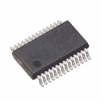
Packaged in 28-Pin Shrink Small Outline
(DB) Package
DB PACKAGE
(TOP VIEW)
VCC
1Y0
1Y1
GND
VCC
1Y2
1Y3
GND
A
VCC
3Y0
GND
VCC
SDATA
1
2
3
4
5
6
7
8
9
10
11
12
13
14
28
27
26
25
24
23
22
21
20
19
18
17
16
15
VCC
2Y3
2Y2
GND
VCC
2Y1
2Y0
GND
OE
VCC
3Y1
GND
GND
SCLOCK
description
The CDC319 is a high-performance clock buffer that distributes one input (A) to 10 outputs (Y) with minimum
skew for clock distribution. The CDC319 operates from a 3.3-V power supply, and is characterized for operation
from 0°C to 70°C.
The device provides a standard mode (100K-bits/s) I2C serial interface for device control. The implementation
is as a slave/receiver. The device address is specified in the I2C device address table. Both of the I2C inputs
(SDATA and SCLOCK) provide integrated pullup resistors (typically 140 kΩ) and are 5-V tolerant.
Three 8-bit I2C registers provide individual enable control for each of the outputs. All outputs default to enabled
at powerup. Each output can be placed in a disabled mode with a low-level output when a low-level control bit
is written to the control register. The registers are write only and must be accessed in sequential order (i.e.,
random access of the registers is not supported).
The CDC319 provides 3-state outputs for testing and debugging purposes. The outputs can be placed in a
high-impedance state via the output-enable (OE) input. When OE is high, all outputs are in the operational state.
When OE is low, the outputs are placed in a high-impedance state. OE provides an integrated pullup resistor.
Please be aware that an important notice concerning availability, standard warranty, and use in critical applications of
Texas Instruments semiconductor products and disclaimers thereto appears at the end of this data sheet.
Copyright 2001, Texas Instruments Incorporated
PRODUCTION DATA information is current as of publication date.
Products conform to specifications per the terms of Texas Instruments
standard warranty. Production processing does not necessarily include
testing of all parameters.
POST OFFICE BOX 655303
• DALLAS, TEXAS 75265
1
�CDC319
1-LINE TO 10-LINE CLOCK DRIVER
WITH I2C CONTROL INTERFACE
SCAS590A – DECEMBER 1997 – REVISED OCTOBER 2001
FUNCTION TABLE
INPUTS
OUTPUTS
OE
A
1Y0–1Y3
2Y0–2Y3
3Y0–3Y1
L
X
Hi-Z
Hi-Z
Hi-Z
H
L
H
H
L
H†
L
H†
H†
L
† The function table assumes that all outputs are enabled via the appropriate I2C
configuration register bit. If the output is disabled via the appropriate configuration bit,
then the output is driven to a low state, regardless of the state of the A input.
logic diagram (positive logic)
20
OE
14
SDATA
I2C
Register
Space
I2C
10
/
2, 3, 6, 7
15
SCLOCK
1Y0–1Y3
22, 23, 26, 27
2Y0–2Y3
9
A
11, 18
3Y0 – 3Y1
Terminal Functions
TERMINAL
NAME
2
NO.
I/O
DESCRIPTION
1Y0–1Y3
2, 3, 6, 7
O
3.3-V SDRAM byte 0 clock outputs
2Y0–2Y3
22, 23, 26, 27
O
3.3-V SDRAM byte 1 clock outputs
3Y0–3Y1
11, 18
O
3.3-V clock outputs provided for feedback control of external PLLs (phase-locked loops)
A
9
I
Clock input
OE
20
I
Output enable. When asserted, OE puts all outputs in a high-impedance state. A nominal
140-kΩ pullup resistor is internally integrated.
SCLOCK
15
I
I2C serial clock input. A nominal 140-kΩ pullup resistor is internally integrated.
SDATA
14
I/O
GND
4, 8, 12, 16,
17, 21, 25
Ground
VCC
1, 5, 10, 13,
19, 24, 28
3.3-V power supply
Bidirectional I2C serial data input/output. A nominal 140-kΩ pullup resistor is internally
integrated.
POST OFFICE BOX 655303
• DALLAS, TEXAS 75265
�CDC319
1-LINE TO 10-LINE CLOCK DRIVER
WITH I2C CONTROL INTERFACE
SCAS590A – DECEMBER 1997 – REVISED OCTOBER 2001
I2C DEVICE ADDRESS
A7
A6
A5
A4
A3
A2
A1
A0 (R/W)
H
H
L
H
L
L
H
—
I2C BYTE 0-BIT DEFINITION†
BIT
DEFINITION
DEFAULT VALUE
7
Reserved
H
6
Reserved
H
5
Reserved
H
4
Reserved
H
3
1Y3 enable (pin 7)
H
2
1Y2 enable (pin 6)
H
1
1Y1 enable (pin 3)
H
0
1Y0 enable (pin 2)
H
† When the value of the bit is high, the output is enabled.
When the value of the bit is low, the output is forced to a
low state. The default value of all bits is high.
I2C BYTE 1-BIT DEFINITION†
BIT
DEFINITION
DEFAULT VALUE
7
2Y3 enable (pin 27)
H
6
2Y2 enable (pin 26)
H
5
2Y1 enable (pin 23)
H
4
2Y0 enable (pin 22)
H
3
Reserved
H
2
Reserved
H
1
Reserved
H
0
Reserved
H
† When the value of the bit is high, the output is enabled.
When the value of the bit is low, the output is forced to a
low state. The default value of all bits is high.
I2C BYTE 2-BIT DEFINITION†
BIT
DEFINITION
DEFAULT VALUE
7
3Y1 enable (pin 18)
H
6
3Y0 enable (pin 11)
H
5
Reserved
H
4
Reserved
H
3
Reserved
H
2
Reserved
H
1
Reserved
H
0
Reserved
H
† When the value of the bit is high, the output is enabled.
When the value of the bit is low, the output is forced to a
low state. The default value of all bits is high.
POST OFFICE BOX 655303
• DALLAS, TEXAS 75265
3
�CDC319
1-LINE TO 10-LINE CLOCK DRIVER
WITH I2C CONTROL INTERFACE
SCAS590A – DECEMBER 1997 – REVISED OCTOBER 2001
absolute maximum ratings over operating free-air temperature range (unless otherwise noted)†
Supply voltage range, VCC . . . . . . . . . . . . . . . . . . . . . . . . . . . . . . . . . . . . . . . . . . . . . . . . . . . . . . . . . –0.5 V to 4.6 V
Input voltage range, VI (see Note 1) . . . . . . . . . . . . . . . . . . . . . . . . . . . . . . . . . . . . . . . . . . . . . . . . . –0.5 V to 4.6 V
Input voltage range, VI (SCLOCK, SDATA) (see Note 1) . . . . . . . . . . . . . . . . . . . . . . . . . . . . . . . –0.5 V to 6.5 V
Output voltage range, VO (SDATA) (see Note 1) . . . . . . . . . . . . . . . . . . . . . . . . . . . . . . . . . . . . . . –0.5 V to 6.5 V
Voltage range applied to any output in the high-impedance or power-off state, VO . . . –0.5 V to VCC + 0.5 V
Current into any output in the low state (except SDATA), IO . . . . . . . . . . . . . . . . . . . . . . . . . . . . . . . . . . . . 48 mA
Current into SDATA in the low state, IO . . . . . . . . . . . . . . . . . . . . . . . . . . . . . . . . . . . . . . . . . . . . . . . . . . . . . 12 mA
Input clamp current, IIK (VI < 0) (SCLOCK) . . . . . . . . . . . . . . . . . . . . . . . . . . . . . . . . . . . . . . . . . . . . . . . . . –50 mA
Output clamp current, IOK (VO < 0) (SDATA) . . . . . . . . . . . . . . . . . . . . . . . . . . . . . . . . . . . . . . . . . . . . . . . –50 mA
Package thermal impedance, θJA (see Note 2) . . . . . . . . . . . . . . . . . . . . . . . . . . . . . . . . . . . . . . . . . . . 120 °C/W
Storage temperature range, Tstg . . . . . . . . . . . . . . . . . . . . . . . . . . . . . . . . . . . . . . . . . . . . . . . . . . . –65°C to 150°C
Lead temperature 1,6 mm (1/16 inch) from case for 10 seconds . . . . . . . . . . . . . . . . . . . . . . . . . . . . . . . . 260_C
† Stresses beyond those listed under “absolute maximum ratings” may cause permanent damage to the device. These are stress ratings only, and
functional operation of the device at these or any other conditions beyond those indicated under “recommended operating conditions” is not
implied. Exposure to absolute-maximum-rated conditions for extended periods may affect device reliability.
NOTES: 1. The input and output negative-voltage ratings may be exceeded if the input and output clamp-current ratings are observed.
2. The package thermal impedance is calculated in accordance with EIA/JEDEC Std JESD51, except for through-hole packages,
which use a trace length of zero.
recommended operating conditions (see Note 3)
MIN
VCC
3.3-V core supply voltage
MAX
UNIT
3.135
3.465
V
2
VCC+0.3
V
2.2
5.5
V
–0.3
0.8
V
0
1.04
V
A, OE
VIH
High-level input voltage
VIL
Low-level input voltage
SDATA, SCLOCK
(see Note 3)
IOH
IOL
High-level output current
Y outputs
– 24
mA
Low-level output current
Y outputs
24
mA
RI
Input resistance to VCC
SDATA, SCLOCK
(see Note 3)
f(SCL)
t(BUS)
SCLOCK frequency
Bus free time
4.7
µs
tsu(START)
th(START)
START setup time
4.7
µs
4
µs
tw(SCLL)
tw(SCLH)
SCLOCK low pulse duration
4.7
µs
tr(SDATA)
tf(SDATA)
SDATA input rise time
tsu(SDATA)
th(SDATA)
SDATA setup time
SDATA hold time
0
ns
tsu(STOP)
TA
STOP setup time
4
µs
Operating free-air temperature
0
SDATA, SCLOCK
(see Note 3)
A, OE
140
kΩ
100
START hold time
SCLOCK high pulse duration
SDATA input fall time
1000
ns
300
ns
250
POST OFFICE BOX 655303
• DALLAS, TEXAS 75265
kHz
µs
4
NOTE 3: The CMOS-level inputs fall within these limits: VIH min = 0.7 × VCC and VIL max = 0.3 × VCC.
4
TYP
ns
70
°C
�CDC319
1-LINE TO 10-LINE CLOCK DRIVER
WITH I2C CONTROL INTERFACE
SCAS590A – DECEMBER 1997 – REVISED OCTOBER 2001
electrical characteristics over recommended operating free-air temperature range (unless
otherwise noted)
PARAMETER
VIK
VOH
VOL
IOH
IOL
TEST CONDITIONS
Input clamp voltage
High-level output voltage
Low-level output voltage
High level output current
High-level
Low-level output current
Y outputs
VCC = 3.135 V,
VCC = 3.135 V,
II = –18 mA
IOH = –1 mA
Y outputs
VCC = 3.135 V,
SDATA
VCC = 3.135
3 135 V
IOL = 1 mA
IOL = 3 mA
SDATA
VCC = 3.135 V,
VCC = 3.135 V,
Y outputs
Y outputs
VCC = 3.3 V,
VCC = 3.465 V,
VCC = 3.135 V,
VCC = 3.3 V,
MIN
TYP
High-level input current
V
0.1
0.4
0.2
0.6
VO = 2 V
VO = 2.6 V
– 54
–126
VO = 3.135 V
VO = 1 V
– 21
IOL = 6 mA
VO = VCC MAX
VCC = 3.465 V,
VO = 0.7 V
VO = 0.4 V
VCC = 3.465 V,
VI = VCC
20
– 46
49
118
23
53
20
ICC
Supply current
∆ICC
Change in supply current
Ci
Input capacitiance
Co
CI/O
µA
–5
VI = GND
SCLOCK, SDATA
Off-state current
mA
58
20
VCC = 3.465 V,
OE
High-impedance-state output current
µA
5
OE
IOZ
Ioff
V
mA
– 60
A
Low-level input current
V
0.4
SCLOCK, SDATA
IIL
UNIT
–1.2
2.4
A
IIH
MAX
SCLOCK, SDATA
VCC = 3.465 V,
VCC = 0 V,
–10
– 50
– 10
– 50
VO = 3.465 V or 0
VI = 0 V to 5.5 V
VCC = 3.465 V,
IO = 0
VCC = 3.135 V to 3.465 V,
One input at VCC – 0.6 V,
All other inputs at VCC or GND
0.2
µA
±10
µA
50
µA
0.5
mA
500
µA
VCC = 3.3 V
VCC = 3.3 V
4
pF
Output capacitance
VI = VCC or GND,
VO = VCC or GND,
6
pF
SDATA I/O capacitance
VI/O = VCC or GND,
VCC = 3.3 V
7
pF
POST OFFICE BOX 655303
• DALLAS, TEXAS 75265
5
�CDC319
1-LINE TO 10-LINE CLOCK DRIVER
WITH I2C CONTROL INTERFACE
SCAS590A – DECEMBER 1997 – REVISED OCTOBER 2001
switching characteristics over recommended operating conditions
PARAMETER
tPLH
Low-to-high level propagation delay time
tPLH
Low-to-high level propagation delay time
tPHL
High-to-low level propagation delay time
tPHL
High-to-low level propagation delay time
tPZH
tPZL
Enable time to the high level
tPHZ
tPLZ
Disable time from the high level
tsk(o)
tsk(p)
tsk(pr)
tr
FROM
TO
A
Y
SCLOCK↓
SDATA
valid
SDATA↑
Y
TEST CONDITIONS
MIN
MAX
1.2
3.6
ns
VCC = 3.3 V ±0.185 V,
See Figure 3
2
µs
VCC = 3.3 V ±0.185 V,
See Figure 3
150
ns
A
Y
3.6
ns
SCLOCK↓
SDATA
valid
VCC = 3.3 V ±0.185 V,
See Figure 3
2
µs
SDATA↑
Y
VCC = 3.3 V ±0.185 V,
See Figure 3
150
ns
OE
Y
47
4.7
ns
Skew time
A
Y
250
ps
Skew time
A
Y
500
ps
Skew time
A
Y
1
ns
1.3
ns
Enable time to the low level
1.2
1
Disable time from the low level
Rise time
tr
Rise time ((see Note 4 and
Figure 3)
tf
Fall time
tf
Fall time ((see Note 4 and
Figure 3)
f
Operating frequency (see Note 5)
Y
0.5
CL = 10 pF
SDATA
CL = 400 pF
Y
SDATA
6
250
0.5
CL = 10 pF
1.3
20
CL = 400 pF
250
CL = 30 pF, TA = 70°C
100
CL = 20 pF, TA = 70°C
125
CL = 15 pF, TA = 70°C
140
NOTES: 4. This parameter has a lower limit than BUS specification. This allows use of series resistors for current spike protection.
5. See Figure 4 (Frequency versus Capacitive Load).
6
UNIT
POST OFFICE BOX 655303
• DALLAS, TEXAS 75265
ns
ns
ns
MHz
�CDC319
1-LINE TO 10-LINE CLOCK DRIVER
WITH I2C CONTROL INTERFACE
SCAS590A – DECEMBER 1997 – REVISED OCTOBER 2001
PARAMETER MEASUREMENT INFORMATION
6V
S1
500 Ω
From Output
Under Test
GND
CL = 30 pF
(see Note A)
S1
Open
6V
GND
TEST
tPLH /tPHL
tPLZ /tPZL
tPHZ /tPZH
Open
500 Ω
tw
LOAD CIRCUIT FOR tpd AND tsk
3V
Input
1.5 V
1.5 V
From Output
Under Test
0V
VOLTAGE WAVEFORMS
CL = 30 pF
(see Note A)
1.5 V
0V
tPHL
2.4 V
0.4 V
tr
1.5 V
0V
tPLZ
1.5 V
tPLH
Output
1.5 V
tPZL
3V
Input
VCC
Output
Enable
(high-level
enabling)
LOAD CIRCUIT FOR tr AND tf
1.5 V
VOH
2.4 V
0.4 V
VOL
tf
≈3V
Output
Waveform 1
S1 at 6 V
(see Note B)
Output
Waveform 2
S1 at GND
(see Note B)
1.5 V
VOL
tPHZ
tPZH
VOLTAGE WAVEFORMS
VOL + 0.3 V
VOH
1.5 V
VOH – 0.3 V
≈0V
VOLTAGE WAVEFORMS
NOTES: A. CL includes probe and jig capacitance.
B. Waveform 1 is for an output with internal conditions such that the output is low except when disabled by the output control.
Waveform 2 is for an output with internal conditions such that the output is high except when disabled by the output control.
C. All input pulses are supplied by generators having the following characteristics: PRR ≤ 10 MHz, ZO = 50 Ω, tr ≤ 2.5 ns, tf ≤ 2.5 ns.
D. The outputs are measured one at a time with one transition per measurement.
Figure 1. Load Circuit and Voltage Waveforms
POST OFFICE BOX 655303
• DALLAS, TEXAS 75265
7
�CDC319
1-LINE TO 10-LINE CLOCK DRIVER
WITH I2C CONTROL INTERFACE
SCAS590A – DECEMBER 1997 – REVISED OCTOBER 2001
PARAMETER MEASUREMENT INFORMATION
A
1Y0
tPHL1
tPLH1
1Y1
tPHL2
tPLH2
1Y2
tPHL3
tPLH3
1Y3
tPHL4
tPLH4
2Y0
tPHL5
tPLH5
2Y1
tPHL6
tPLH6
2Y2
tPHL7
tPLH7
2Y3
tPHL8
tPLH8
3Y0
tPHL9
tPLH9
3Y1
tPHL10
tPLH10
NOTES: A. Output skew, tsk(o), is calculated as the greater of:
– The difference between the fastest and slowest of tPLHn (n = 1:10)
– The difference between the fastest and slowest of tPHLn (n = 1:10)
B. Pulse skew, tsk(p), is calculated as the greater of |tPLHn – tPHLn| (n = 1:10).
C. Process skew, tsk(pr), is calculated as the greater of:
– The difference between the fastest and slowest of tPLHn (n = 1:10) across multiple devices under identical operating conditions
– The difference between the fastest and slowest of tPHLn (n = 1:10) across multiple devices under identical operating conditions
Figure 2. Waveforms for Calculation of tsk(o), tsk(p), tsk(pr)
8
POST OFFICE BOX 655303
• DALLAS, TEXAS 75265
�CDC319
1-LINE TO 10-LINE CLOCK DRIVER
WITH I2C CONTROL INTERFACE
SCAS590A – DECEMBER 1997 – REVISED OCTOBER 2001
PARAMETER MEASUREMENT INFORMATION
VO = 3.3 V
RL = 1 kΩ
DUT
CL = 10 pF or
CL = 400 pF
GND
TEST CIRCUIT
4 to 6 Bytes for Complete Device
Programming
Start
Condition
(S)
Bit 7
MSB
Bit 0
LSB
(R/W)
Bit 6
tw(SCLL)
Acknowledge
(A)
Stop
Condition
(P)
tsu(START)
tw(SCLH)
0.7 VCC
0.3 VCC
SCLOCK
tsu(START)
tr
tPHL
tf
t(BUS)
tPLH
0.7 VCC
0.3 VCC
SDATA
tf(SDATA)
th(START)
tr(SDATA)
th(SDATA)
tsu(SDATA)
tsu(STOP)
Repeat Start
Condition
(see Note A)
Start or
Repeat Start
Condition
Stop Condition
VOLTAGE WAVEFORMS
BYTE
DESCRIPTION
1
I2C address
2
Command (dummy value, ignored)
3
Byte count (dummy value, ignored)
I2C data byte 0
4
5
6
I2C data byte 1
I2C data byte 2
NOTES: A. The repeat start condition is not supported.
B. All input pulses are supplied by generators having the following characteristics: PRR ≤ 100 kHz, ZO = 50 Ω, tr ≥ 10 ns, tf ≥ 10 ns.
Figure 3. Propagation Delay Times, tr and tf
POST OFFICE BOX 655303
• DALLAS, TEXAS 75265
9
�CDC319
1-LINE TO 10-LINE CLOCK DRIVER
WITH I2C CONTROL INTERFACE
SCAS590A – DECEMBER 1997 – REVISED OCTOBER 2001
CAPACITIVE LOAD
vs
SUPPORTED MAXIMUM CLOCK FREQUENCY
60
55
CL – Capaccitive Load – pF
50
TA = 55°C
TJ = 130°C
VDD = 3.465 V
45
40
35
30
TA = 70°C
TJ = 130°C
VDD = 3.6 V
25
20
15
10
30
40
50
60
70
80
90
100
110
120
f – Supported Maximum Clock Frequency – MHz
130
140
150
NOTES: A. With a total capacitive load of 20 pF for each output, the CDC319 is capable of running up to about 125 MHz. A lower capacitive
load will allow higher application frequencies, up to 133 MHz (140 MHz).
B. CPD for the CDC319 is about 25 pF per output (21 pF if CL < 20 pF)
P(total) = VDD2 × CPD × FO × N + (VOH – VOL)2 × CL × FO × N + DC load
where:
N = number of switching outputs
FO = clock frequency
Package thermal impedance (junction-to-ambient) = 92.4°C/W
Maximum junction temperature = 150°C (