CDC421AXXX
www.ti.com ....................................................................................................................................................................................................... SCAS875 – MAY 2009
Fully-Integrated, Fixed-Frequency, Low-Jitter
Crystal Oscillator Clock Generator
FEATURES
APPLICATIONS
• Single 3.3-V Supply
• High-Performance Clock Generator,
Incorporating Crystal Oscillator Circuitry with
Integrated Frequency Synthesizer
• Low Output Jitter: As low as 380 fs (RMS
integrated between 10 kHz to 20 MHz)
• Low Phase Noise at 312.5 MHz:
– Less than –120 dBc/Hz at 10 kHz and
–147 dBc/Hz at 10-MHz offset from carrier
• Supports Crystal or LVCMOS Input
Frequencies at 31.25 MHz, 33.33 MHz, and
35.42 MHz
• Output Frequencies: 100 MHz, 106.25 MHz,
125 MHz, 156.25 MHz, 212.5 MHz, 250 MHz, and
312.5 MHz
• Differential Low-Voltage Positive Emitter
Coupled Logic (LVPECL) Outputs
• Fully-Integrated Voltage-Controlled Oscillator
(VCO): Runs from 1.75 GHz to 2.35 GHz
• Typical Power Consumption: 300 mW
• Chip Enable Control Pin
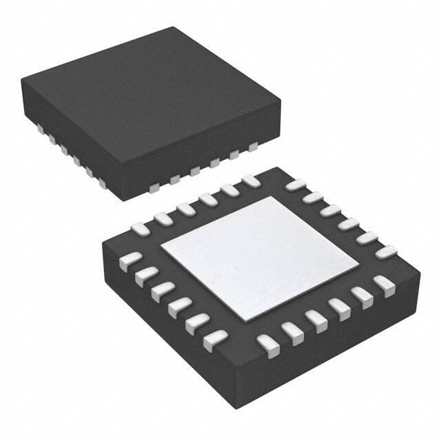
• Available in 4-mm × 4-mm QFN-24 Package
• ESD Protection Exceeds 2 kV (HBM)
• Industrial Temperature Range: –40°C to +85°C
•
1
2
Low-Cost, Low-Jitter Frequency Multiplier
DESCRIPTION
The
CDC421Axxx
is
a
high-performance,
low-phase-noise clock generator. It has an integrated
low-noise, LC-based voltage-controlled oscillator
(VCO) that operates within the 1.75 GHz to 2.35 GHz
frequency range. It has an integrated crystal oscillator
that operates in conjunction with an external AT-cut
crystal to produce a stable frequency reference for a
phase-locked
loop
(PLL)-based
frequency
synthesizer. The output frequency (fOUT) is
proportional to the frequency of the input crystal
(fXTAL).
The device operates in 3.3-V supply environment and
is characterized for operation from –40°C to +85°C.
The CDC421Axxx is available in a QFN-24 4-mm ×
4-mm package.
The CDC421Axxx differs from the CDC421xxx in
the following ways:
• Device Startup
The CDC421Axxx has an improved startup circuit
to enable correct operation for all power-supply
ramp times.
VCO
LVPECL
Feedback
Divider
CLK
Output Divider
External
Crystal
Prescaler
Crystal
Oscillator
Input
PFD/Charge Pump
Loop Filter
NCLK
CDC421Axxx
1
2
Please be aware that an important notice concerning availability, standard warranty, and use in critical applications of Texas
Instruments semiconductor products and disclaimers thereto appears at the end of this data sheet.
All trademarks are the property of their respective owners.
PRODUCTION DATA information is current as of publication date.
Products conform to specifications per the terms of the Texas
Instruments standard warranty. Production processing does not
necessarily include testing of all parameters.
Copyright © 2009, Texas Instruments Incorporated
�CDC421AXXX
SCAS875 – MAY 2009 ....................................................................................................................................................................................................... www.ti.com
This integrated circuit can be damaged by ESD. Texas Instruments recommends that all integrated circuits be handled with
appropriate precautions. Failure to observe proper handling and installation procedures can cause damage.
ESD damage can range from subtle performance degradation to complete device failure. Precision integrated circuits may be more
susceptible to damage because very small parametric changes could cause the device not to meet its published specifications.
AVAILABLE OPTIONS (1)
PRODUCT
INPUT
FREQUENCY OR
CRYSTAL
VALUE (MHz)
OUTPUT
FREQUENCY FOR
SPECIFIED INPUT
FREQUENCY (MHz)
PACKAGELEAD
PACKAGE
MARKING
CDC421A100
33.3333
100.00
QFN-24
421A100
CDC421A106
35.4167
106.25
QFN-24
421A106
CDC421A125
31.2500
125.00
QFN-24
421A125
CDC421A156
31.2500
156.25
QFN-24
421A156
CDC421A212
35.4167
212.50
QFN-24
421A212
CDC421A250
31.2500
250.00
QFN-24
421A250
CDC421A312
31.2500
312.50
QFN-24
421A312
(1)
ORDERING
INFORMATION
TRANSPORT MEDIA,
QUANTITY
CDC421A100RGET
Tape and reel, 250
CDC421A100RGER
Tape and reel, 2500
CDC421A106RGET
Tape and reel, 250
CDC421A106RGER
Tape and reel, 2500
CDC421A125RGET
Tape and reel, 250
CDC421A125RGER
Tape and reel, 2500
CDC421A156RGET
Tape and reel, 250
CDC421A156RGER
Tape and reel, 2500
CDC421A212RGET
Tape and reel, 250
CDC421A212RGER
Tape and reel, 2500
CDC421A250RGET
Tape and reel, 250
CDC421A250RGER
Tape and reel, 2500
CDC421A312RGET
Tape and reel, 250
CDC421A312RGER
Tape and reel, 2500
For the most current specifications and package information, see the Package Option Addendum located at the end of this data sheet or
refer to our web site at www.ti.com.
ABSOLUTE MAXIMUM RATINGS (1)
Over operating free-air temperature range (unless otherwise noted).
PARAMETER
Supply voltage (2)
VCC
(2)
VI
Voltage range for all other input pins
IO
Output current for LVPECL
ESD
Electrostatic discharge (HBM)
TA
Specified free-air temperature range (no airflow)
TJ
Maximum junction temperature
TSTG
Storage temperature range
(1)
(2)
CDC421Axxx
UNIT
–0.5 to 4.6
V
–0.5 to VCC to +0.5
V
–50
mA
2
kV
–40 to +85
°C
+125
°C
–65 to +150
°C
Stresses beyond those listed under absolute maximum ratings may cause permanent damage to the device. These are stress ratings
only, and functional operation of the device at these or any other conditions beyond those indicated under recommended operating
condition is not implied. Exposure to absolute-maximum-rated conditions for extended periods may affect device reliability.
All voltage values are with respect to network ground terminal.
RECOMMENDED OPERATING CONDITIONS
Over operating free-air temperature range (unless otherwise noted).
MIN
NOM
MAX
UNIT
VCC
Supply voltage
3.0
3.30
3.60
V
TA
Ambient temperature (no airflow, no heatsink)
–40
+85
°C
2
Submit Documentation Feedback
Copyright © 2009, Texas Instruments Incorporated
�CDC421AXXX
www.ti.com ....................................................................................................................................................................................................... SCAS875 – MAY 2009
ELECTRICAL CHARACTERISTICS
Over recommended operating conditions (unless otherwise noted).
CDC421Axxx
PARAMETER
VCC
Supply voltage
IVCC
Total current
TEST CONDITIONS
MIN
TYP
MAX
UNIT
3.00
3.30
3.60
V
91
110
mA
100
312.5
MHz
LVPECL OUTPUT
fCLK
Output frequency
VOH
LVPECL high-level output voltage
VCC – 1.20
VCC – 0.81
VOL
LVPECL low-level output voltage
VCC – 2.17
VCC – 1.36
|VOD|
LVPECL differential output voltage
407
1076
tR
Output rise time
20% to 80% of VOUT(PP)
230
tF
Output fall time
20% to 80% of VOUT(PP)
230
Duty cycle of the output waveform
tj
RMS jitter
45
V
mV
ps
ps
55
10 kHz to 20 MHz
V
%
1 ps, RMS
LVCMOS INPUT
VIL, CMOS
Low-level CMOS input voltage
VCC = 3.3 V
VIH, CMOS
High-level CMOS input voltage
VCC = 3.3 V
0.3 × VCC
IL, CMOS
Low-level CMOS input current
VCC = VCC, max, VIL = 0.0 V
–200
µA
IH, CMOS
High-level CMOS input current
VCC = VCC, min, VIH = 3.7 V
200
µA
0.7 × VCC
V
V
FUNCTIONAL BLOCK DIAGRAM
XIN 1
XIN 2
Crystal
Oscillator
Loop Filter
PFD/
Charge Pump
VCO
Prescaler
Output
Divider
Feedback
Divider
Figure 1. CDC421Axxx: High-Level Block Diagram
Copyright © 2009, Texas Instruments Incorporated
Submit Documentation Feedback
3
�CDC421AXXX
SCAS875 – MAY 2009 ....................................................................................................................................................................................................... www.ti.com
DEVICE INFORMATION
NC
NC
XIN2
XIN1
NC
NC
24
23
22
21
20
19
RGE PACKAGE
QFN-24
(TOP VIEW)
CE
1
18
NC
NC
2
17
VCC
NC
3
16
VCC
NC
4
15
NC
NC
5
14
NC
NC
6
13
NC
8
9
10
11
12
GND
GND
OUTP
NC
NC
OUTN
7
Thermal Pad
(Bottom Side)
CDC421AXXX
CDC421Axxx Pin Descriptions
TERMINAL
4
NAME
NO.
TYPE
ESD
PROTECTION
VCC
16, 17
Power
Y
3.3-V power supply
GND
8, 9
Ground
Y
Ground
XIN1
21
I
Y
XIN2
22
I
N
In crystal input mode, connect XIN1 to one end of the crystal and XIN2 to the
other end of the crystal.
In LVCMOS single-ended driven mode, XIN1 (pin 21) acts as input reference
and XIN2 should connect to GND.
CE
1
I
Y
Chip enable (LVCMOS input)
CE = 1 enables the device and the outputs.
CE = 0 disables all current sources (LVPECLP = LVPECLN = Hi-Z).
OUTP
10
O
Y
High-speed positive differential LVPECL output. (Outputs are enabled by CE
pin.)
OUTN
7
O
Y
High-speed negative differential LVPECL output. (Outputs are enabled by CE
pin.)
NC
2–6, 11–15,
18–20, 23, 24
—
Y
Submit Documentation Feedback
DESCRIPTION
TI test pin. Do not connect; leave floating.
Copyright © 2009, Texas Instruments Incorporated
�CDC421AXXX
www.ti.com ....................................................................................................................................................................................................... SCAS875 – MAY 2009
JITTER CHARACTERISTICS IN INPUT CLOCK MODE
Jitter characterization tests are performed using an LVCMOS input signal driving the CDC421Axxx device, as
Figure 2 illustrates.
0.1 pF
Phase Noise
Analyzer
XIN 1
CDC421Axxx
50 W
100 pF
XIN 2
150 W
50 W
150 W
Figure 2. Jitter Test Configuration for an LVTTL Input Driving CDC421Axxx
When the CDC421Axxx is referenced by an external, clean LVCMOS input of 31.25 MHz, 33.33 MHz, and
35.4167 MHz, Table 1 to Table 7 list the measured SSB phase noise of all the outputs supported by the
CDC421Axxx device (100 MHz, 106.25 MHz, 125 MHz, 156.25 MHz, 212.5 MHz, 250 MHz, and 312.5 MHz)
from 100 Hz to 20 MHz from the carrier.
Table 1. Phase Noise Data with LVCMOS Input of 33.3333 MHz and LVPECL Output at 100.00 MHz (1)
PARAMETER
MIN
TYP
MAX
UNIT
phn100
Phase noise at 100 Hz
–111
dBc/Hz
phn1k
Phase noise at 1 kHz
–121
dBc/Hz
phn10k
Phase noise at 10 kHz
–131
dBc/Hz
phn100k
Phase noise at 100 kHz
–133
dBc/Hz
phn1M
Phase noise at 1 MHz
–142
dBc/Hz
phn10M
Phase noise at 10 MHz
–149
dBc/Hz
phn20M
Phase noise at 20 MHz
–149
dBc/Hz
JRMS
RMS jitter integrated from 12 kHz to 20 MHz
507
fs
Tj
Total jitter
35.33
ps
Dj
Deterministic jitter
11.54
ps
(1)
Phase noise specifications under following conditions: input frequency = 33.3333 MHz, output frequency = 100.00 MHz.
Table 2. Phase Noise Data with LVCMOS Input of 35.4167 MHz and LVPECL Output at 106.25 MHz (1)
PARAMETER
MIN
TYP
MAX
UNIT
phn100
Phase noise at 100 Hz
–112
dBc/Hz
phn1k
Phase noise at 1 kHz
–121
dBc/Hz
phn10k
Phase noise at 10 kHz
–125
dBc/Hz
phn100k
Phase noise at 100 kHz
–129
dBc/Hz
phn1M
Phase noise at 1 MHz
–142
dBc/Hz
phn10M
Phase noise at 10 MHz
–151
dBc/Hz
phn20M
Phase noise at 20 MHz
–151
dBc/Hz
JRMS
RMS jitter integrated from 12 kHz to 20 MHz
530
fs
Tj
Total jitter
30.39
ps
Dj
Deterministic jitter
11
ps
(1)
Phase noise specifications under following conditions: input frequency = 35.4167 MHz, output frequency = 106.25 MHz.
Copyright © 2009, Texas Instruments Incorporated
Submit Documentation Feedback
5
�CDC421AXXX
SCAS875 – MAY 2009 ....................................................................................................................................................................................................... www.ti.com
Table 3. Phase Noise Data with LVCMOS Input of 31.2500 MHz and LVPECL Output at 125.00 MHz (1)
PARAMETER
MIN
TYP
MAX
UNIT
phn100
Phase noise at 100 Hz
–108
dBc/Hz
phn1k
Phase noise at 1 kHz
–118
dBc/Hz
phn10k
Phase noise at 10 kHz
–127
dBc/Hz
phn100k
Phase noise at 100 kHz
–130
dBc/Hz
phn1M
Phase noise at 1 MHz
–139
dBc/Hz
phn10M
Phase noise at 10 MHz
–147
dBc/Hz
phn20M
Phase noise at 20 MHz
–147
dBc/Hz
JRMS
RMS jitter integrated from 12 kHz to 20 MHz
529
fs
Tj
Total jitter
47.47
ps
Dj
Deterministic jitter
25.2
ps
(1)
Phase noise specifications under following conditions: input frequency = 31.2500 MHz, output frequency = 125.00 MHz.
Table 4. Phase Noise Data with LVCMOS Input of 31.2500 MHz and LVPECL Output at 156.25 MHz (1)
PARAMETER
MIN
TYP
MAX
UNIT
phn100
Phase noise at 100 Hz
–106
dBc/Hz
phn1k
Phase noise at 1 kHz
–117
dBc/Hz
phn10k
Phase noise at 10 kHz
–126
dBc/Hz
phn100k
Phase noise at 100 kHz
–128
dBc/Hz
phn1M
Phase noise at 1 MHz
–139
dBc/Hz
phn10M
Phase noise at 10 MHz
–147
dBc/Hz
phn20M
Phase noise at 20 MHz
–147
dBc/Hz
JRMS
RMS jitter integrated from 12 kHz to 20 MHz
472
fs
Tj
Total jitter
31.54
ps
Dj
Deterministic jitter
9.12
ps
(1)
Phase noise specifications under following conditions: input frequency = 31.2500 MHz, output frequency = 156.25 MHz.
Table 5. Phase Noise Data with LVCMOS Input of 35.4167 MHz and LVPECL Output at 212.50 MHz (1)
PARAMETER
MIN
TYP
MAX
UNIT
phn100
Phase noise at 100 Hz
–105
dBc/Hz
phn1k
Phase noise at 1 kHz
–115
dBc/Hz
phn10k
Phase noise at 10 kHz
–119
dBc/Hz
phn100k
Phase noise at 100 kHz
–123
dBc/Hz
phn1M
Phase noise at 1 MHz
–135
dBc/Hz
phn10M
Phase noise at 10 MHz
–148
dBc/Hz
phn20M
Phase noise at 20 MHz
–148
dBc/Hz
JRMS
RMS jitter integrated from 12 kHz to 20 MHz
512
fs
Tj
Total jitter
33.96
ps
Dj
Deterministic jitter
13.78
ps
(1)
6
Phase noise specifications under following conditions: input frequency = 35.4167 MHz, output frequency = 212.50 MHz.
Submit Documentation Feedback
Copyright © 2009, Texas Instruments Incorporated
�CDC421AXXX
www.ti.com ....................................................................................................................................................................................................... SCAS875 – MAY 2009
Table 6. Phase Noise Data with LVCMOS Input of 31.2500 MHz and LVPECL Output at 250.00 MHz (1)
PARAMETER
MIN
TYP
MAX
UNIT
phn100
Phase noise at 100 Hz
–105
dBc/Hz
phn1k
Phase noise at 1 kHz
–112
dBc/Hz
phn10k
Phase noise at 10 kHz
–121
dBc/Hz
phn100k
Phase noise at 100 kHz
–124
dBc/Hz
phn1M
Phase noise at 1 MHz
–134
dBc/Hz
phn10M
Phase noise at 10 MHz
–148
dBc/Hz
phn20M
Phase noise at 20 MHz
–149
dBc/Hz
JRMS
RMS jitter integrated from 12 kHz to 20 MHz
420
fs
Tj
Total jitter
36.98
ps
Dj
Deterministic jitter
18.52
ps
(1)
Phase noise specifications under following conditions: input frequency = 31.2500 MHz, output frequency = 250.00 MHz.
Table 7. Phase Noise Data with LVCMOS Input of 31.2500 MHz and LVPECL Output at 312.50 MHz (1)
PARAMETER
MIN
TYP
MAX
UNIT
phn100
Phase noise at 100 Hz
–102
dBc/Hz
phn1k
Phase noise at 1 kHz
–111
dBc/Hz
phn10k
Phase noise at 10 kHz
–120
dBc/Hz
phn100k
Phase noise at 100 kHz
–123
dBc/Hz
phn1M
Phase noise at 1 MHz
–135
dBc/Hz
phn10M
Phase noise at 10 MHz
–147
dBc/Hz
phn20M
Phase noise at 20 MHz
–147
dBc/Hz
JRMS
RMS jitter integrated from 12 kHz to 20 MHz
378
fs
Tj
Total jitter
29.82
ps
Dj
Deterministic jitter
11
ps
(1)
Phase noise specifications under following conditions: input frequency = 31.2500 MHz, output frequency = 312.50 MHz.
Copyright © 2009, Texas Instruments Incorporated
Submit Documentation Feedback
7
�PACKAGE OPTION ADDENDUM
www.ti.com
10-Dec-2020
PACKAGING INFORMATION
Orderable Device
Status
(1)
Package Type Package Pins Package
Drawing
Qty
Eco Plan
(2)
Lead finish/
Ball material
MSL Peak Temp
Op Temp (°C)
Device Marking
(3)
(4/5)
(6)
CDC421A100RGER
ACTIVE
VQFN
RGE
24
3000
RoHS & Green
NIPDAU
Level-2-260C-1 YEAR
-40 to 85
421A
100
CDC421A100RGET
ACTIVE
VQFN
RGE
24
250
RoHS & Green
NIPDAU
Level-2-260C-1 YEAR
-40 to 85
421A
100
CDC421A106RGER
ACTIVE
VQFN
RGE
24
3000
RoHS & Green
NIPDAU
Level-2-260C-1 YEAR
-40 to 85
421A
106
CDC421A106RGET
ACTIVE
VQFN
RGE
24
250
RoHS & Green
NIPDAU
Level-2-260C-1 YEAR
-40 to 85
421A
106
CDC421A125RGER
ACTIVE
VQFN
RGE
24
3000
RoHS & Green
NIPDAU
Level-2-260C-1 YEAR
-40 to 85
421A
125
CDC421A125RGET
ACTIVE
VQFN
RGE
24
250
RoHS & Green
NIPDAU
Level-2-260C-1 YEAR
-40 to 85
421A
125
CDC421A156RGER
ACTIVE
VQFN
RGE
24
3000
RoHS & Green
NIPDAU
Level-2-260C-1 YEAR
-40 to 85
421A
156
CDC421A156RGET
ACTIVE
VQFN
RGE
24
250
RoHS & Green
NIPDAU
Level-2-260C-1 YEAR
-40 to 85
421A
156
CDC421A212RGER
ACTIVE
VQFN
RGE
24
3000
RoHS & Green
NIPDAU
Level-2-260C-1 YEAR
-40 to 85
421A
212
CDC421A212RGET
ACTIVE
VQFN
RGE
24
250
RoHS & Green
NIPDAU
Level-2-260C-1 YEAR
-40 to 85
421A
212
CDC421A250RGER
ACTIVE
VQFN
RGE
24
3000
RoHS & Green
NIPDAU
Level-2-260C-1 YEAR
-40 to 85
421A
250
CDC421A250RGET
ACTIVE
VQFN
RGE
24
250
RoHS & Green
NIPDAU
Level-2-260C-1 YEAR
-40 to 85
421A
250
CDC421A312RGER
ACTIVE
VQFN
RGE
24
3000
RoHS & Green
NIPDAU
Level-2-260C-1 YEAR
-40 to 85
421A
312
CDC421A312RGET
ACTIVE
VQFN
RGE
24
250
RoHS & Green
NIPDAU
Level-2-260C-1 YEAR
-40 to 85
421A
312
(1)
The marketing status values are defined as follows:
ACTIVE: Product device recommended for new designs.
LIFEBUY: TI has announced that the device will be discontinued, and a lifetime-buy period is in effect.
NRND: Not recommended for new designs. Device is in production to support existing customers, but TI does not recommend using this part in a new design.
PREVIEW: Device has been announced but is not in production. Samples may or may not be available.
OBSOLETE: TI has discontinued the production of the device.
Addendum-Page 1
Samples
�PACKAGE OPTION ADDENDUM
www.ti.com
10-Dec-2020
(2)
RoHS: TI defines "RoHS" to mean semiconductor products that are compliant with the current EU RoHS requirements for all 10 RoHS substances, including the requirement that RoHS substance
do not exceed 0.1% by weight in homogeneous materials. Where designed to be soldered at high temperatures, "RoHS" products are suitable for use in specified lead-free processes. TI may
reference these types of products as "Pb-Free".
RoHS Exempt: TI defines "RoHS Exempt" to mean products that contain lead but are compliant with EU RoHS pursuant to a specific EU RoHS exemption.
Green: TI defines "Green" to mean the content of Chlorine (Cl) and Bromine (Br) based flame retardants meet JS709B low halogen requirements of


 工商网监
湘ICP备2023018690号
工商网监
湘ICP备2023018690号
