��������
�
��
�� �� �� ���
������ ��� �������
�
�
�� ��������� ����� ��� ����� ��������
SCAS813A − AUGUST 2005 − REVISED DECEMBER 2005
D Low Jitter Clock Multiplier by x4, x6, x8.
D
D
D
D
D
D
D
D
D
D
D
D
Input Frequency Range (19 MHz to
125 MHz). Supports Output Frequency
From 150 MHz to 500 MHz
Fail-Safe Power Up Initialization
Low Jitter Clock Divider by /2, /3, /4. Input
Frequency Range (50 MHz to 125 MHz).
Supports Ranges of Output Frequency
From 12.5 MHz to 62.5 MHz
2.6 mUI Programmable Bidirectional Delay
Steps
Typical 8-ps Phase Jitter (12 kHz to 20 MHz)
at 500 MHz
Typical 2.1-ps RMS Period Jitter (Entire
Frequency Band) at 500 MHz
One Single-Ended Input and One
Differential Output Pair
Output Can Drive LVPECL, LVDS, and
LVTTL
Three Power Operating Modes to Minimize
Power
Low Power Consumption (Typical 200 mW
at 500 MHz)
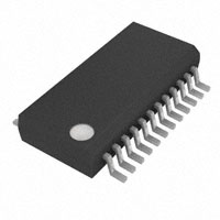
Packaged in a Shrink Small-Outline
Package (DBQ)
No External Components Required for PLL
Spread Spectrum Clock Tracking Ability to
Reduce EMI
D Applications: Video Graphics, Gaming
Products, Datacom, Telecom
D Accepts LVCMOS, LVTTL Inputs for
D
D
REFCLK Terminal
Accepts Other Single-Ended Signal Levels
at REFCLK Terminal by Programming
Proper VDDREF Voltage Level (For
Example, HSTL 1.5 if VDDREF = 1.6 V)
Supports Industrial Temperature Range of
−40°C to 85°C
DBQ PACKAGE
(TOP VIEW)
VDDREF
REFCLK
VDDP
GNDP
GND
LEADLAG
DLYCTRL
GNDPA
VDDPA
VDDPD
STOPB
PWRDNB
1
24
2
23
3
22
4
21
5
20
6
19
7
18
8
17
9
16
10
15
11
14
12
13
P0
P1
VDDO
GNDO
CLKOUT
NC
CLKOUTB
GNDO
VDDO
MULT0/DIV0
MULT1/DIV1
P2
NC − No internal connection
description
The CDC5801A device provides clock multiplication and division from a single-ended reference clock
(REFCLK) to a differential output pair (CLKOUT/CLKOUTB). The multiply and divide terminals (MULT/DIV0:1)
provide selection for frequency multiplication and division ratios, generating CLKOUT/CLOUTKB frequencies
ranging from 12.5 MHz to 500 MHz with a clock input reference (REFCLK) ranging from 19 MHz to 125 MHz.
See Table 1 and Table 2 for detail frequency support.
The implemented phase aligner provides the possibility to phase align (zero delay) between
CLKOUT/CLKOUTB and REFCLK or any other CLK in the system by feeding the clocks that need to be aligned
to the DLYCTRL and the LEADLAG terminals.
The phase aligner also allows the user to delay or advance the CLKOUT/CLKOUTB with steps of 2.6 mUI (unit
interval). For every rising edge on the DLYCTRL terminal, the output clocks are delayed by 2.6-mUI step size
as long as there is low on the LEADLAG terminal. Similarly, for every rising edge on the DLYCTRL terminal, the
output clocks are advanced by 2.6-mUI step size as long as there is high on the LEADLAG terminal. The
CDC5801A has a fail-safe power up initialization state-machine which supports proper operation under all
power up conditions. As the phase between REFCLK and CLKOUT/CLKOUTB is random after power up, the
application may implement a self calibration routine at power up to produce a certain phase start position, before
programming a fixed delay with the clock on the DLYCTRL terminal.
Please be aware that an important notice concerning availability, standard warranty, and use in critical applications of
Texas Instruments semiconductor products and disclaimers thereto appears at the end of this data sheet.
Copyright 2005, Texas Instruments Incorporated
�� ���
� � ��
� �����!"#��� �$ %&��'�# "$ �� (&)*�%"#��� +"#',
���+&%#$ %�����! #� $('%���%"#���$ ('� #-' #'�!$ ��
'."$ ��$#�&!'�#$
$#"�+"�+ /"��"�#0, ���+&%#��� (��%'$$��1 +�'$ ��# �'%'$$"��*0 ��%*&+'
#'$#��1 �� "** ("�"!'#'�$,
POST OFFICE BOX 655303
• DALLAS, TEXAS 75265
1
���������
�
��
�� �� �� ���
������ ��� �������
�
�
�� ��������� ����� ��� ����� ��������
SCAS813A − AUGUST 2005 − REVISED DECEMBER 2005
Depending on the selection of the mode terminals (P0:2), the device behaves as a multiplier (by 4, 6, or 8) with
the phase aligner bypassed or as a multiplier or divider with programmable delay and phase aligner functionality.
Through the select terminals (P0:2) user can also bypass the phase aligner and the PLL (test mode) and output
the REFCLK directly on the CLKOUT/CLKOUTB terminals. Through P0:2 terminals the outputs could be in a
high impedance state. This device has another unique capability to be able to function with a wide band of
voltages on the REFCLK terminal by varying the voltage on the VDDREF terminal.
The CDC5801A has a fail-safe power up initialization state-machine which supports proper operation under all
power up conditions.
The CDC5801A device is characterized for operation over free-air temperatures of −40°C to 85°C.
functional block diagram
PWRDWNB
P0
P1
P2
STOPB
Control Logic
PLLCLK
Phase Aligner
Bypass MUX
PLL
REFCLK
CLKOUT
B
Phase
Aligner
Divider
Ratio
VDDREF/2
φD
A
VDDPD/2
2
2
MULT0/DIV0
MULT1/DIV1
DLYCTRL
POST OFFICE BOX 655303
LEADLAG
• DALLAS, TEXAS 75265
CLKOUTB
���������
�
��
�� �� �� ���
������ ��� �������
�
�
�� ��������� ����� ��� ����� ��������
SCAS813A − AUGUST 2005 − REVISED DECEMBER 2005
FUNCTION TABLE†
MODE
P0
P1
P2
CLKOUT/CLKOUTB
Multiplication with programmable
delay and phase alignment active‡
0
0
0
REFCLK multiplied by ratio per Table 1 selected by MULT/DIV terminals. Outputs
are delayed or advanced based on DLYCTRL and LEADLAG terminal
configuration.
Division with programmable delay
and phase alignment active ‡
0
0
1
REFCLK divided by ratio per Table 2 selected by MULT/DIV terminals. Outputs
are delayed or advanced based on DLYCTRL and LEADLAG terminal
configuration.
Multiplication only mode (phase
aligner bypassed) §
1
0
0
In this mode one can only multiply as per Table 1. Programmable delay capability
and divider capability is deactivated. PLL is running.
Test mode
1
1
0
PLL and phase aligner both bypassed. REFCLK is directly channeled to output.
Hi-Z mode
0
1
X
Hi-Z
† X = don’t care, Hi-Z = high impedance
‡ Please see Table 4 and Table 5 for explanation for the programmability and phase alignment functions.
§ In this mode the DLYCTRL and LEADLAG terminals must be strapped high or low. Lowest possible jitter is achieved in this mode, but a delay
of 200 ps to 2 ns expected typically from REFCLK to CLKOUT depending on the output frequency.
Terminal Functions
TERMINAL
NAME
NO.
I/O
DESCRIPTION
CLKOUT
20
O
Output clock
CLKOUTB
18
O
Output clock (complement)
DLYCTRL
7
I
Every rising edge on this terminal delays/advances the CLKOUT/CLKOUTB signal by 1/384th of the
CLKOUT/CLKOUTB period. (e.g., for a 90 degree delay or advancement one needs to provide 96 rising
edges). See Table 4.
GND
5
GND for VDDREF and VDDPD
GNDO
17, 21
GNDP
4
GNDPA
8
LEADLAG
6
I
Decides if the output clock is delayed or advanced with respect to REFCLK. See Table 4.
MULT0/DIV0
15
I
PLL multiplier and divider select
MULT1/DIV1
14
I
PLL multiplier and divider select
NC
19
PWRDNB
12
I
Active low power down state, CLKOUT/CLKOUTB goes low
P0
24
I
Mode control, see the Function Table
P1
23
I
Mode control, see the Function Table
P2
13
I
Mode control, see the Function Table
REFCLK
2
I
Reference input clock
STOPB
11
I
Active low output disabler, PLL and PA still running, CLKOUT and CLKOUTB goes to a dc value as per Table 3
VDDPA
VDDPD
9
I
Supply voltage for phase aligner
10
I
Reference voltage for the DLYCTRL, LEADLAG terminals and STOPB function
1
I
Reference voltage for REFCLK
16, 22
I
Supply voltage for the output terminals (CLKOUT, CLKOUTB)
3
I
Supply voltage for PLL
VDDREF
VDDO
VDDP
GND for clock output terminals (CLKOUT, CLKOUTB)
GND for PLL
GND for phase aligner
Not used
POST OFFICE BOX 655303
• DALLAS, TEXAS 75265
3
���������
�
��
�� �� �� ���
������ ��� �������
�
�
�� ��������� ����� ��� ����� ��������
SCAS813A − AUGUST 2005 − REVISED DECEMBER 2005
PLL divider/multiplier selection
Table 1 and Table 2 list the supported REFCLK and BUSCLK (CLKOUT/CLKOUTB) frequencies.
Table 1. Multiplication Ratios (P0:2 = 000 or 100)
REFCLK
(MHZ)
MULTIPLICATION
RATIO
BUSCLK
(MHZ)
0
38−125
4
152−500
1
25−83.3
6
150−500
1
19−62.5
8
152−500
MULT0
MULT1
0
0
1
Table 2. Divider Ratio (P0:2 = 001)
MULT0
MULT1
REFCLK
(MHZ)
DIVISION
RATIO
BUSCLK(1)
(MHZ)
0
0
100−125
2
50−62.5
1
0
75−93
3
25−31
1
1
50−62
4
12.5−15.5
† BUSCLK will be undefined until a valid reference clock is available at REFCLK. After applying
REFCLK, the PLL requires stabilization time to achieve phase lock.
Table 3. Clock Output Driver States
STATE
PWRDNB
STOPB
CLKOUT
CLKOUTB
Powerdown
0
X
GND
GND
CLK stop
1
0
Normal
1
1
VO, STOP
As per Function Table
VO, STOP
As per Function Table
Table 4. Programmable Delay and Phase Alignment
DLYCTRL
LEADLAG
Each rising edge†
Each rising edge†
1
CLKOUT AND CLKOUTB
Will be advanced by one step size (see Table 5)
0
Will be delayed by one step size (see Table 5)
† For every 32nd edge, there are one or two edges the phase aligner does not update. Therefore,
CLKOUT phase is not updated on every 32nd edge.
Table 5. Clock Output Driver States
FUNCTIONALITY
STEP SIZE
Multiply by 4, 6, 8
CLKOUT period/384 (for example, 6.5 ps at 400 MHz)
Divide by 2
CLKOUT period/3072 (for example, 6.5 ps at 50 MHz)
Divide by 3
CLKOUT period/6144 (for example, 6.5 ps at 25 MHz)
Divide by 4
CLKOUT period/12288 (for example, 6.5 ps at 12.5 MHz)
NOTE: The frequency of the DLYCTRL terminal must always be equal or less than the
frequency of the LEADLAG terminal.
4
POST OFFICE BOX 655303
• DALLAS, TEXAS 75265
���������
�
��
�� �� �� ���
������ ��� �������
�
�
�� ��������� ����� ��� ����� ��������
SCAS813A − AUGUST 2005 − REVISED DECEMBER 2005
absolute maximum ratings over operating free-air temperature (unless otherwise noted)†
Supply voltage range, VDD (see Note 1) . . . . . . . . . . . . . . . . . . . . . . . . . . . . . . . . . . . . . . . . . . . . . . −0.5 V to 4 V
Output voltage range, VO, at any output terminal . . . . . . . . . . . . . . . . . . . . . . . . . . . . . . . . −0.5 V to VDD + 0.5 V
Input voltage range,VI, at any input terminal . . . . . . . . . . . . . . . . . . . . . . . . . . . . . . . . . . . . −0.5 V to VDD + 0.5 V
Continuous total power dissipation . . . . . . . . . . . . . . . . . . . . . . . . . . . . . . . . . . . . . . see Dissipation Rating Table
Operating free-air temperature range, TA . . . . . . . . . . . . . . . . . . . . . . . . . . . . . . . . . . . . . . . . . . . . −40°C to 85°C
Storage temperature range, Tstg . . . . . . . . . . . . . . . . . . . . . . . . . . . . . . . . . . . . . . . . . . . . . . . . . . . −65°C to 150°C
Lead temperature 1,6 mm (1/16 inch) from case for 10 seconds . . . . . . . . . . . . . . . . . . . . . . . . . . . . . . . 260°C
† Stresses beyond those listed under “absolute maximum ratings” may cause permanent damage to the device. These are stress ratings only, and
functional operation of the device at these or any other conditions beyond those indicated under “recommended operating conditions” is not
implied. Exposure to absolute-maximum-rated conditions for extended periods may affect device reliability.
NOTE 1: All voltage values are with respect to the GND terminals.
DISSIPATION RATING TABLE
PACKAGE
TA ≤ 25°C
POWER RATING
DERATING FACTOR
ABOVE TA = 25°C‡
TA = 85°C
POWER RATING
DBQ
1400 mW
11 mW/°C
740 mW
‡ This is the inverse of the junction-to-ambient thermal resistance when board-mounted and with
no air flow.
recommended operating conditions
Supply voltage, VDD (VDDP, VDDPA, VDDO)
MIN
NOM
MAX
3
3.3
3.6
0.7 × VDD
High-level input voltage, VIH (CMOS)
REFCLK low-level input voltage, VIL
0.7 × VDDREF
REFCLK high-level input voltage, VIH
Input signal high voltage, VIH (STOPB, DLYCTRL, LEADLAG)
0.7 × VDDPD
Input reference voltage for (REFCLK) (VDDREF)
1.235
Input reference voltage for (DLYCTRL and LEADLAG) (VDDPD)
1.235
V
V
V
High-level output current, IOH
Low-level output current, IOL
Operating free-air temperature, TA
V
V
0.3 × VDDPD
Input signal low voltage, VIL (STOPB, DLYCTRL, LEADLAG)
V
V
0.3 × VDD
0.3 × VDDREF
Low-level input voltage, VIL (CMOS)
UNIT
−40
VDD
VDD
V
−16
mA
16
mA
85
°C
V
timing requirements
MIN
Input frequency of modulation, fmod (if driven by SSC CLKIN)
MAX
33
Modulation index (nonlinear maximum 0.5%)
UNIT
kHz
0.6%
Input slew rate, SR
1
4
Input duty cycle on REFCLK
40%
60%
Input frequency on REFCLK
19
125
MHz
200
MHz
400
MHz
Allowable frequency on DLYCTRL
Allowable frequency on LEADLAG
Allowable duty cycle on DLYCTRL and LEADLAG
POST OFFICE BOX 655303
25%
• DALLAS, TEXAS 75265
V/ns
75%
5
���������
�
��
�� �� �� ���
������ ��� �������
�
�
�� ��������� ����� ��� ����� ��������
SCAS813A − AUGUST 2005 − REVISED DECEMBER 2005
electrical characteristics over recommended operating free-air temperature range (unless
otherwise noted)
TEST CONDITIONS†
PARAMETER
VO(STOP)
Output voltage during CLK stop
mode
See Figure 1
VOX
VO
Output crossing-point voltage
See Figure 1 and Figure 4
Output voltage swing (VOH − VOL)
See Figure 1
VIK
Input clamp voltage
VDD = 3 V,
II = −18 mA
See Figure 1, VDD = 3 to 3.6 V
VOH
High-level output voltage
VOL
Low-level output voltage
IOH
IOL
VDD = 3 V,
IOH = −16 mA
See Figure 1, VDD = 3 to 3.6 V
High-level output current
Low-level output current
VDD = 3 V,
VDD = 3.135 V,
IOL = 16 mA
VO = 1 V
VDD = 3.3 V,
VDD = 3.465 V,
VO = 1.65 V
VO = 3.135 V
VDD = 3.135 V,
VDD = 3.3 V,
VDD = 3.465 V,
VO = 1.95 V
VO = 1.65 V
High-impedance-state output
current
P0 = 0,
IOZ(STOP)
High-impedance-state output
current during CLK stop
Stop = 0, VO = GND or VDD
IOZ(PD)
High-impedance-state output
current in power-down state
PWRDNB = 0,
VO = GND or VDD
IIH
IIL
ZO
Low-level input
current
Output impedance
(single ended)
Reference current
TYP‡
MAX
2
V
0.5VDDO−0.2
1.7
0.5VDDO+0.2
2.9
V
−1.2
V
2.0
V
2.2
0.3
0.6
0.5
−32
−14.5
mA
−21
61.5
65
25.5
P1 = 1
−10
mA
36
± 10
µA
± 100
µA
100
µA
VDD = 3.6 V,
VI = VDD
10
PWRDNB,
P0:2, MULT/
DIV0:1
VDD = 3.6 V,
VI = VDD
10
REFCLK,
STOPB
VDD = 3.6 V,
VI = 0
−10
PWRDNB,
P0:2, MULT/
DIV0:1
VDD = 3.6 V,
VI = 0
−10
µA
µA
High state
RI at IO −14.5 mA to −16.5 mA
15
35
50
Low state
RI at IO 14.5 mA to 16.5 mA
11
17
35
VDDREF,
VDDPD
VDD = 3.6 V
Input capacitance
CO
Output capacitance
IDD(PD)
Supply current in power-down state
V
−52
−51
43
V
2.6
REFCLK,
STOPB
CI
UNIT
1.1
VO = 0.4 V
IOZ
High-level input
current
MIN
Ω
PWRDNB = 0
50
µA
PWRDNB = 1
0.5
mA
VI = VDD or GND
VO = VDD or GND
2
pF
3
pF
REFCLK = 0 MHz to 100 MHz,
PWDNB = 0,
STOPB = 1
150
µA
IDD(CLKSTOP) Supply current in CLK stop state
BUSCLK configured for 500 MHz
40
mA
IDD(NORMAL) Supply current in normal state
BUSCLK = 500 MHz
P0:2 = 000; load see Figure 1
70
mA
† VDD refers to any of the following; VDDPA, VDDPD, VDDREF, VDDO, and VDDP
‡ All typical values are at VDD = 3.3 V, TA = 25°C.
6
POST OFFICE BOX 655303
• DALLAS, TEXAS 75265
���������
�
��
�� �� �� ���
������ ��� �������
�
�
�� ��������� ����� ��� ����� ��������
SCAS813A − AUGUST 2005 − REVISED DECEMBER 2005
jitter specification over recommended operating free-air temperature range and VCC (unless
otherwise noted)
PARAMETER
t(jitter)
(Multiplication only mode. Phase alignment
and programmable delay features are not
selected (PA bypass). See Figure 2.)
TEST CONDITIONS
155 MHz
Period RMS (1Σ jitter, full frequency band)
Period p-p
Phase jitter (accumulated, 12 kHz to 20 MHz)
Cycle-to-cycle (+)
Cycle-to-cycle (−)
6
40
50
27
27
ps
200 MHz
Period RMS (1Σ jitter, full frequency band)
Period p-p
Phase jitter (accumulated, 12 kHz to 20 MHz)
Phase jitter (accumulated, 50 kHz to 80 MHz)
Cycle-to-cycle (+)
Cycle-to-cycle (−)
5.5
36
36
36
23
23
ps
312 MHz
Period RMS (1Σ jitter, full frequency band)
Period p-p
Phase jitter (accumulated, 12 kHz to 20 MHz)
Phase jitter (accumulated, 50 kHz to 80 MHz)
Cycle-to-cycle (+)
Cycle-to-cycle (−)
3
20
18
18
17
17
ps
400 MHz
Period RMS (1Σ jitter, full frequency band)
Period p-p
Phase jitter (accumulated, 12 kHz to 20 MHz)
Phase jitter (accumulated, 50 kHz to 80 MHz)
Cycle-to-cycle (+)
Cycle-to-cycle (−)
2.3
17
12
12
15
15
ps
500 MHz
Period RMS (1Σ jitter, full frequency band)
Period p-p
Phase jitter (accumulated, 12 kHz to 20 MHz)
Phase jitter (accumulated, 50 kHz to 80 MHz)
Cycle-to-cycle (+)
Cycle-to-cycle (−)
2.1
16
8
8
14
14
ps
155 MHz
Period RMS (1Σ jitter, full frequency band)
Period p-p
Phase jitter (accumulated, 12 kHz to 20 MHz)
Cycle-to-cycle (+)
Cycle-to-cycle (−)
9
70
50
50
50
ps
200 MHz
Period RMS (1Σ jitter, full frequency band)
Period p-p
Phase jitter (accumulated, 12 kHz to 20 MHz)
Phase jitter (accumulated, 50 kHz to 80 MHz)
Cycle-to-cycle (+)
Cycle-to-cycle (−)
7
55
36
36
40
40
ps
312 MHz
Period RMS (1Σ jitter, full frequency band)
Period p-p
Phase jitter (accumulated, 12 kHz to 20 MHz)
Phase jitter (accumulated, 50 kHz to 80 MHz)
Cycle-to-cycle (+)
Cycle-to-cycle (−)
4
35
18
18
30
30
ps
400 MHz
Period RMS (1Σ jitter, full frequency band)
Period p-p
Phase jitter (accumulated, 12 kHz to 20 MHz)
Phase jitter (accumulated, 50 kHz to 80 MHz)
Cycle-to-cycle (+)
Cycle-to-cycle (−)
3.1
27
13
13
25
25
ps
t(jitter)
(Multiplication with phase alignment and
programmable delay features selected. See
Figure 2.)
MIN
TYP†
CLKOUT
MAX
UNIT
† All typical values are at VDD = 3.3 V, TA = 25°C.
POST OFFICE BOX 655303
• DALLAS, TEXAS 75265
7
���������
�
��
�� �� �� ���
������ ��� �������
�
�
�� ��������� ����� ��� ����� ��������
SCAS813A − AUGUST 2005 − REVISED DECEMBER 2005
jitter specification over recommended operating free-air temperature range and VCC (unless
otherwise noted) (continued)
PARAMETER
t(jitter)
(Multiplication with phase alignment and
programmable delay features selected.
See Figure 2.)
CLKOUT
MAX
UNIT
500 MHz
ps
12.5 MHz
Period RMS (1Σ jitter, full frequency band)
Period p-p
Cycle-to-cycle (+)
Cycle-to-cycle (−)
12
75
55
55
ps
15.5 MHz
Period RMS (1Σ jitter, full frequency band)
Period p-p
Cycle-to-cycle (+)
Cycle-to-cycle (−)
8
50
38
38
ps
25 MHz
Period RMS (1Σ jitter, full frequency band)
Period p-p
Cycle-to-cycle (+)
Cycle-to-cycle (−)
7.5
50
35
35
ps
31 MHz
Period RMS (1Σ jitter, full frequency band)
Period p-p
Cycle-to-cycle (+)
Cycle-to-cycle (−)
5.5
30
23
23
ps
50 MHz
Period RMS (1Σ jitter, full frequency band)
Period p-p
Phase jitter (accumulated, 12 kHz to 20 MHz)
Cycle-to-cycle (+)
Cycle-to-cycle (−)
8
40
12
30
30
ps
62.5 MHz
Period RMS (1Σ jitter, full frequency band)
Period p-p
Phase jitter (accumulated, 12 kHz to 20 MHz)
Cycle-to-cycle (+)
Cycle-to-cycle (−)
5.5
28
9
24
24
ps
12.5 MHz
Period RMS (1Σ jitter, full frequency band)
Period p-p
Cycle-to-cycle (+)
Cycle-to-cycle (−)
12.5
80
55
55
ps
15.5 MHz
Period RMS (1Σ jitter, full frequency band)
Period p-p
Cycle-to-cycle (+)
Cycle-to-cycle (−)
8.5
55
38
38
ps
25 MHz
Period RMS (1Σ jitter, full frequency band)
Period p-p
Cycle-to-cycle (+)
Cycle-to-cycle (−)
10
60
35
35
ps
31 MHz
Period RMS (1Σ jitter, full frequency band)
Period p-p
Cycle-to-cycle (+)
Cycle-to-cycle (−)
7
40
23
23
ps
MULT0:1 = 00
(Divider
ratio = 2)
MULT0:1 = 11
(Divider
ratio = 4)
MULT0:1 = 10
(Divider
ratio = 3)
8
TYP†
2.9
24
9
9
20
20
MULT0:1 = 10
(Divider
ratio = 3)
t(jitter)
(Divider mode with
phase alignment and
programmable delay
features selected. See
Figure 2.)
MIN
Period RMS (1Σ jitter, full frequency band)
Period p-p
Phase jitter (accumulated, 12 kHz to 20 MHz)
Phase jitter (accumulated, 50 kHz to 80 MHz)
Cycle-to-cycle (+)
Cycle-to-cycle (−)
MULT0:1 = 11
(Divider
ratio = 4)
t(jitter)
(Divider mode with
phase aligner not active:
DLYCTRL =LEADLAG =
0 or 1. See Figure 2.)
TEST CONDITIONS
POST OFFICE BOX 655303
• DALLAS, TEXAS 75265
���������
�
��
�� �� �� ���
������ ��� �������
�
�
�� ��������� ����� ��� ����� ��������
SCAS813A − AUGUST 2005 − REVISED DECEMBER 2005
jitter specification over recommended operating free-air temperature range and VCC (unless
otherwise noted) (continued)
PARAMETER
t(jitter)
(Divider mode with
phase alignment and
programmable delay
features selected. See
Figure 2.)
CLKOUT
TEST CONDITIONS
MIN
TYP†
MAX
UNIT
50 MHz
Period RMS (1Σ jitter, full frequency band)
Period p-p
Phase jitter (accumulated, 12 kHz to 20 MHz)
Cycle-to-cycle (+)
Cycle-to-cycle (−)
9
50
13
35
35
ps
62.5 MHz
Period RMS (1Σ jitter, full frequency band)
Period p-p
Phase jitter (accumulated, 12 kHz to 20 MHz)
Cycle-to-cycle (+)
Cycle-to-cycle (−)
6.5
30
10
26
26
ps
MULT0:1 = 00
(Divider
ratio = 2)
† All typical values are at VDD = 3.3 V, TA = 25°C.
switching characteristics over recommended operating free-air temperature range (unless
otherwise noted)
PARAMETER
TEST CONDITIONS
t(DC)
Output duty cycle
See Figure 3
tr, tf
Output rise and fall times (measured at 20%−80% of
output voltage)
See Figure 5 and Figure 1
MIN
TYP†
MAX
45%
55%
150
350
UNIT
ps
† All typical values are at VDD = 3.3 V, TA = 25°C.
POST OFFICE BOX 655303
• DALLAS, TEXAS 75265
9
���������
�
��
�� �� �� ���
������ ��� �������
�
�
�� ��������� ����� ��� ����� ��������
SCAS813A − AUGUST 2005 − REVISED DECEMBER 2005
state transition latency specifications
PARAMETER
t(powerup)
t(VDDpowerup)
t(MULT)
t(CLKON)
Delay time, PWRDNB↑ to CLKOUT/
CLKOUTB output settled (excluding
t(DISTLOCK))
FROM
TO
Powerdown
Normal
TEST
CONDITIONS
MIN
TYP†
MAX
3
See Figure 6
ms
Delay time, PWRDNB↑ to internal PLL and
clock are on and settled
3
Delay time, power up to CLKOUT/CLKOUTB
output settled
3
VDD
Delay time, power up to internal PLL and
clock are on and settled
MULT0 and MULT1 change to CLKOUT/
CLKOUTB output resettled (excluding
t(DISTLOCK))
STOPB↑ to CLKOUT/CLKOUTB glitch-free
clock edges
UNIT
Normal
See Figure 6
ms
3
Normal
Normal
See Figure 7
1
ms
CLK Stop
Normal
See Figure 8
10
ns
CLK Stop
Normal
See Figure 8
20
cycles
t(CLKSETL)
STOPB↑ to CLKOUT/CLKOUTB output
settled to within 50 ps of the phase before
STOPB was disabled
t(CLKOFF)
STOPB↓ to CLKOUT/CLKOUTB output disabled
Normal
CLK
Stop
See Figure 8
5
ns
t(powerdown)
Delay time, PWRDNB↓ to the device in the
power-down mode
Normal
Power−
down
See Figure 6
1
ms
t(STOP)
Maximum time in CLKSTOP (STOPB = 0)
before reentering normal mode (STOPB = 1)
STOPB
Normal
See Figure 8
100
µs
t(ON)
Minimum time in normal mode (STOPB = 1)
before reentering CLKSTOP (STOPB = 0)
Normal
CLK
stop
See Figure 8
100
† All typical values are at VDD = 3.3 V, TA = 25°C.
PARAMETER MEASUREMENT INFORMATION
CLKOUT
50 Ω
VCM
50 Ω
10 pF
CLKOUTB
Figure 1. Test Load and Voltage Definitions (VO(STOP), VOX, VOH, VOL)
10
POST OFFICE BOX 655303
• DALLAS, TEXAS 75265
ms
���������
�
��
�� �� �� ���
������ ��� �������
�
�
�� ��������� ����� ��� ����� ��������
SCAS813A − AUGUST 2005 − REVISED DECEMBER 2005
PARAMETER MEASUREMENT INFORMATION
CLKOUTB
CLKOUT
tcycle,i
tcycle,i+1
Cycle-to-Cycle Jitter = | tcycle,i − tcycle,i+r| Over 1000 Consecutive Cycles
Figure 2. Cycle-to-Cycle Jitter
CLKOUT
CLKOUTB
tpw+
tcycle
Duty Cycle = (tpw+/tcycle)
Figure 3. Output Duty Cycle
CLKOUT
VX+
VX, nom
VX−
CLKOUTB
Figure 4. Crossing-Point Voltage
VOH
80%
20%
VOL
tr
tf
Figure 5. Voltage Waveforms
PWRDNB
CLKOUT/
CLKOUTB
ÎÎÎÎÎÎÎ
ÎÎÎÎÎÎÎ
ÎÎÎÎÎÎÎ
Figure 6. PWRDNB Transition Timings
POST OFFICE BOX 655303
ÎÎ
ÎÎ
ÎÎ
t(power down)
t(power up)
• DALLAS, TEXAS 75265
11
���������
�
��
�� �� �� ���
������ ��� �������
�
�
�� ��������� ����� ��� ����� ��������
SCAS813A − AUGUST 2005 − REVISED DECEMBER 2005
PARAMETER MEASUREMENT INFORMATION
MULT0 and/or MULT1
ÎÎÎÎÎÎÎÎ
ÎÎÎÎÎÎÎÎ
CLKOUT/
CLKOUTB
t(MULT)
Figure 7. MULT Transition Timings
t(ON)
t(STOP)
STOPB
t(CLKSETL)
t(CLKON)
(see Note A)
CLKOUT/
CLKOUTB
ÎÎÎÎ
ÎÎÎÎ
ÎÎÎÎ
Output Clock
Not Specified
Glitches OK
Clock Enabled
and Glitch Free
ÎÎ
ÎÎ
ÎÎ
Clock Output Settled
Within 50 ps of the
Phase Before Disabled
NOTE A: Vref = VO ± 200 mV
Figure 8. STOPB Transition Timings
12
POST OFFICE BOX 655303
• DALLAS, TEXAS 75265
t(CLKOFF)
(see Note A)
���������
�
��
�� �� �� ���
������ ��� �������
�
�
�� ��������� ����� ��� ����� ��������
SCAS813A − AUGUST 2005 − REVISED DECEMBER 2005
Z = 50 Ω ; Length = L1
CDCVF2310
Clock Buffer
3.3 V
CDC5801
VDDREF A
3.3 V
REFCLK
VDDP
GNDP
GND
3.3 V
CLK
Outputs are Phase Aligned
Between the Two Buffers
P0
P1
VDDO
GNDO
3.3 V
CDCVF2310
Clock Buffer
CLKOUT
LEADLAG
NC
DLYCTRL
CLKOUTB
Z = 50 Ω
20 R
GNDPA
GNDO
VDDPA
VDDPD
VDDO
MULT0/DIV0
3.3 V
STOPB
MULT1/DIV1
3.3 V
PWRDNB
CLK
155.52 MHz
Z = 50 Ω
Z = 50 Ω
19.44 MHz
Very Low Jitter
19.44 MHz
P2
Z = 50 Ω ; Length = L1
Figure 9. Using the CDC5801A Device as a Multiplier by 8 and Aligning Two Different Clocks
POST OFFICE BOX 655303
• DALLAS, TEXAS 75265
13
�PACKAGE MATERIALS INFORMATION
www.ti.com
3-Jun-2022
TAPE AND REEL INFORMATION
REEL DIMENSIONS
TAPE DIMENSIONS
K0
P1
B0 W
Reel
Diameter
Cavity
A0
B0
K0
W
P1
A0
Dimension designed to accommodate the component width
Dimension designed to accommodate the component length
Dimension designed to accommodate the component thickness
Overall width of the carrier tape
Pitch between successive cavity centers
Reel Width (W1)
QUADRANT ASSIGNMENTS FOR PIN 1 ORIENTATION IN TAPE
Sprocket Holes
Q1
Q2
Q1
Q2
Q3
Q4
Q3
Q4
User Direction of Feed
Pocket Quadrants
*All dimensions are nominal
Device
CDC5801ADBQR
Package Package Pins
Type Drawing
SSOP
DBQ
24
SPQ
Reel
Reel
A0
Diameter Width (mm)
(mm) W1 (mm)
2500
330.0
16.4
Pack Materials-Page 1
6.5
B0
(mm)
K0
(mm)
P1
(mm)
9.0
2.1
8.0
W
Pin1
(mm) Quadrant
16.0
Q1
�PACKAGE MATERIALS INFORMATION
www.ti.com
3-Jun-2022
TAPE AND REEL BOX DIMENSIONS
Width (mm)
W
L
H
*All dimensions are nominal
Device
Package Type
Package Drawing
Pins
SPQ
Length (mm)
Width (mm)
Height (mm)
CDC5801ADBQR
SSOP
DBQ
24
2500
356.0
356.0
35.0
Pack Materials-Page 2
��IMPORTANT NOTICE AND DISCLAIMER
TI PROVIDES TECHNICAL AND RELIABILITY DATA (INCLUDING DATA SHEETS), DESIGN RESOURCES (INCLUDING REFERENCE
DESIGNS), APPLICATION OR OTHER DESIGN ADVICE, WEB TOOLS, SAFETY INFORMATION, AND OTHER RESOURCES “AS IS”
AND WITH ALL FAULTS, AND DISCLAIMS ALL WARRANTIES, EXPRESS AND IMPLIED, INCLUDING WITHOUT LIMITATION ANY
IMPLIED WARRANTIES OF MERCHANTABILITY, FITNESS FOR A PARTICULAR PURPOSE OR NON-INFRINGEMENT OF THIRD
PARTY INTELLECTUAL PROPERTY RIGHTS.
These resources are intended for skilled developers designing with TI products. You are solely responsible for (1) selecting the appropriate
TI products for your application, (2) designing, validating and testing your application, and (3) ensuring your application meets applicable
standards, and any other safety, security, regulatory or other requirements.
These resources are subject to change without notice. TI grants you permission to use these resources only for development of an
application that uses the TI products described in the resource. Other reproduction and display of these resources is prohibited. No license
is granted to any other TI intellectual property right or to any third party intellectual property right. TI disclaims responsibility for, and you
will fully indemnify TI and its representatives against, any claims, damages, costs, losses, and liabilities arising out of your use of these
resources.
TI’s products are provided subject to TI’s Terms of Sale or other applicable terms available either on ti.com or provided in conjunction with
such TI products. TI’s provision of these resources does not expand or otherwise alter TI’s applicable warranties or warranty disclaimers for
TI products.
TI objects to and rejects any additional or different terms you may have proposed. IMPORTANT NOTICE
Mailing Address: Texas Instruments, Post Office Box 655303, Dallas, Texas 75265
Copyright © 2022, Texas Instruments Incorporated
�


 工商网监
湘ICP备2023018690号
工商网监
湘ICP备2023018690号
