�������
����
��
���������� ����� ����
������ ��� ������ �������
SCAS685L− DECEMBER 2002 − REVISED JUNE 2009
D High Performance 1:5 PLL Clock
D
D
D
CTRL_
CLK
CTRL_
DATA
CP_OUT
OPA_IN
7
8
OPA_IP OPA_OUT
STATUS_
LOCK
GND
GND
GND
GND
C
I_REF
GND
AVCC
AVCC
AVCC
AVCC
AVCC
STATUS_
REF
D VCXO_IN
GND
GND
GND
GND
GND
VCC
STATUS_
VCXO
E
VCXO_IN
B
GND
VCC
VCC
VCC
VCC
VCC
F
Y0
GND
GND
GND
GND
GND
VCC
Y4B
G
Y0B
VCC
VCC
VCC
VCC
VCC
VCC
Y4
H
NPD
Y1
Y1B
Y2
Y2B
Y3
Y3B
NRESET
VCC
STATUS_LOCK
AVCC
GND
OPA_OUT
GND
OPA_IP
GND
AVCC
REF_IN
36
25
37
24
GND
REF_IN
AVCC
STATUS_REF
AVCC
STATUS_VCXO
I_REF
VCC
Top View
VCC
VCC
Thermal Pad
must be
soldered to
GND
VCXO_IN
description
6
B
OPA_IN
D
D
D
5
AVCC
D
D
4
CP_OUT
D
3
CTRL_DATA
D
D
A CTRL_LE
2
CTRL_CLK
D
D
1
NC
D
TERMINAL ASSIGNMENTS
(TOP VIEW)
CTRL_LE
D
Synchronizer
Two Clock Inputs: VCXO_IN Clock Is
Synchronized To REF_IN Clock
Synchronizes Frequencies Up To 800 MHz
(VCXO_IN)
Supports Five Differential LVPECL Outputs
Each Output Frequency Is Selectable By
x1, /2, /4, /8, /16
All Outputs Are Synchronized
Integrated Low-Noise OPA For External
Low-Pass Filter
Efficient Jitter Screening From Low PLL
Loop Bandwidth
Low-Phase Noise Characteristic
Programmable Delay For Phase
Adjustments
Predivider Loop BW Adjustment
SPI Controllable Division Setting
Power-Up Control Forces LVPECL Outputs
to 3-State at VCC < 1.5 V
3.3-V Power Supply
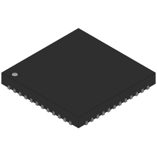
Packaged In 64-Pin BGA (0,8 mm Pitch −
ZVA) or 48-Pin QFN (RGZ)
Industrial Temperature Range –40°C
To 85°C
VCXO_INB
VCC
VCC
Y3B
Y3
VCC
VCC
Y2
Y2B
VCC
Y1B
Y1
VCC
NPD
VCC
Y4B
The CDC7005 is a high-performance, low-phase
VCC
Y4
noise, and low-skew clock synthesizer and jitter
Y0
VCC
cleaner that synchronizes the voltage controlled
Y0B
NRESET
crystal oscillator (VCXO) frequency to the
VCC
VCC
reference clock. The programmable predividers
48
13
1
12
M and N give a high flexibility to the frequency ratio
of the reference clock to VCXO: VCXO_IN/
REF_IN = (NxP)/M. The VCXO_IN clock operates
up to 800 MHz. Through the selection of external
VCXO and loop filter components, the PLL loop bandwidth and damping factor can be adjusted to meet different
system requirements. Each of the five differential LVPECL outputs are programmable by the serial peripheral
interface (SPI). The SPI allows individual control of frequency and enable/disable state of each output. The
device operates in 3.3-V environment. The built-in latches ensure that all outputs are synchronized.
VCC
The CDC7005 is characterized for operation from –40°C to 85°C.
Please be aware that an important notice concerning availability, standard warranty, and use in critical applications of
Texas Instruments semiconductor products and disclaimers thereto appears at the end of this data sheet.
Copyright 2009, Texas Instruments Incorporated
��������� ���� ���!"#$%�!� �& '("")�% $& !� *(+,�'$%�!� -$%)�
"!-('%& '!��!"# %! &*)'���'$%�!�& *)" %.) %)"#& !� �)/$& ��&%"(#)�%&
&%$�-$"- 0$""$�%1�
"!-('%�!� *"!')&&��2 -!)& �!% �)')&&$"�,1 ��',(-)
%)&%��2 !� $,, *$"$#)%)"&�
POST OFFICE BOX 655303
• DALLAS, TEXAS 75265
1
��������
����
��
���������� ����� ����
������ ��� ������ �������
SCAS685L− DECEMBER 2002 − REVISED JUNE 2009
functional block diagram
OPA_IN
−
OPA_OUT
OPA
+
OPA_IP
STATUS_REF
STATUS_VCXO
STATUS_LOCK
HOLD
REF_IN
LVCMOS
Input
Prgm Divider
M
Prgm Delay
M
Prgm Divider
N
Prgm Delay
N
PFD
CP_OUT
Charge
Pump
CTRL_LE
VI
Reference
SPI LOGIC
CTRL_DATA
I_REF
CTRL_CLK
PECL-TOLVTTL
NPD
NRESET
MUX_SEL
VCXO_IN
VCXO_INB
PECL
Input
Y0
/1
PECL
MUX0
PECL
Latch
PECL
Output
PECL
MUX1
PECL
Latch
PECL
Output
PECL
MUX2
PECL
Latch
PECL
Output
PECL
MUX3
PECL
Latch
PECL
Output
PECL
MUX4
PECL
Latch
PECL
Output
Y0B
/2
Y1
/4
Y1B
/8
Y2
/16
Y2B
P Divider
Y3
Y3B
Y4
2
POST OFFICE BOX 655303
• DALLAS, TEXAS 75265
Y4B
��������
����
��
���������� ����� ����
������ ��� ������ �������
SCAS685L− DECEMBER 2002 − REVISED JUNE 2009
Pin Functions
PIN
NAME
TYPE
DESCRIPTION
BGA
QFN
AVCC
CP_OUT
C3, C4, C5, C6, C7
27, 30, 32, 38, 39
Power
A4
31
O
Charge pump output
CTRL_LE
A1
36
I
LVCMOS input, control load enable for serial programmable
interface (SPI) with hysteresis. Unused or floating inputs must be
tied to proper logic level. It is recommend to use a 20kΩ or larger
pull−up resistor to VCC.
CTRL_CLK
A2
35
I
LVCMOS input, serial control clock input for SPI, with hysteresis.
Unused or floating inputs must be tied to proper logic level. It is
recommend to use a 20kΩ or larger pull−up resistor to VCC.
CTRL_DATA
A3
33
I
LVCMOS input, serial control data input for SPI, with hysteresis.
Unused or floating inputs must be tied to proper logic level. It is
recommend to use a 20kΩ or larger pull−up resistor to VCC.
B2, B3, B4, B5, B6,
B7, B8, C2, D2, D3,
D4, D5, D6, E2, F2,
F3, F4, F5, F6
Thermal pad and
pin 24
Ground
C1
40
O
Current path for external reference resistor (12 kΩ ±1%) to support
an accurate charge pump current, optional. Do not use any
capacitor across this resistor to prevent noise coupling via this
node. If internal 12 kΩ is selected (default setting), this pin can be
left open.
GND
I_REF
NC
3.3-V analog power supply
Ground
−
34
−
Not connected
NPD
H1
1
I
LVCMOS input, asynchronous power down (PD) signal active on
low. Switches all current sources off, resets all dividers to default
values, and 3-states all outputs. Has an internal 150-kΩ pullup
resistor.
Note 2: It is recommended to ramp up NPD at the same time with
VCC and AVCC or later. The ramp up rate should not be faster than
the ramp up rate of VCC and AVCC
NRESET
H8
14
I
LVCMOS input, asynchronous reset signal active on low. Resets
the counter of all dividers to zero keeping its divider values the
same. It has an internal 150-kΩ pullup resistor. Yx outputs are
switched low during reset.
OPA_IN
A5
29
I
Inverting input of the op amp, see Note 1
OPA_OUT
A7
26
O
Output of the op amp, see Note 1
OPA_IP
A6
28
I
Noninverting input of the op amp, see Note 1
REF_IN
B1
37
I
LVCMOS reference clock input
STATUS_LOCK
A8
25
O
This pin is high if the PLL lock definition is valid. PLL lock definition
means the rising edge of REF_IN clock and VCXO_IN clock for
PFD are inside the lock detect window for at least five successive
input clock cycles. If the rising edge of REF_IN clock and VCXO_IN
clock are out of the selected lock detect window, this pin will be low,
but it does not refer to the real lock condition of the PLL. This
means, that i.e. due to a strong jitter at REF_IN or VCXO_IN
STATUS_LOCK can be low, even if the PLL is in Lock. The PLL is
in lock for sure, if STATUS_LOCK is high.See Table 8 and Figure 4.
STATUS_REF
C8
23
O
LVCMOS output provides the status of the reference input
(frequencies above 3.5 MHz are interpreted as valid clock, active
high)
STATUS_VCXO
D8
22
O
LVCMOS outputs provides the status of the VCXO input
(frequencies above 10 MHz are interpreted as valid clock, active
high)
POST OFFICE BOX 655303
• DALLAS, TEXAS 75265
3
��������
����
��
���������� ����� ����
������ ��� ������ �������
SCAS685L− DECEMBER 2002 − REVISED JUNE 2009
VCC
D7, E3, E4, E5, E6,
E7, E8, F7, G2, G3,
G4, G5, G6, G7
2, 5, 6, 9, 10, 13,
15, 18, 19, 20,
21, 41, 44, 45, 48
Power
VCXO_IN
D1
42
I
VCXO LVPECL input
VCXO_INB
E1
43
I
Complementary VCXO LVPECL input
F1, H2, H4, H6, G8
46, 3, 7, 11, 16
O
LVPECL output
Y[0:4]
3.3-V supply
VCC and AVCC should have always same supply voltage
Y[0:4]B
G1, H3, H5, H7, F8
47, 4, 8, 12, 17
O
Complementary LVPECL output
NOTE 1: If the internal operational amplifier is not used, these pins can be left open.
SPI control interface
The serial interface of the CDC7005 is a simple SPI-compatible interface for writing to the registers of the device.
It consists of three control lines: CTRL_CLK, CTRL_DATA, and CTRL_LE. There are four 32-bit wide registers,
which can be addressed by the two LSBs of a transferred word (bit 0 and bit 1). Every transmitted word must
have 32 bits, starting with MSB first. Each word can be written separately. It is recommended to program Word
0, Word 1, Word 2 and Word 3 right after power up and NPD becomes HIGH. The transfer is initiated with the
falling edge of CTRL_LE; as long as CTRL_LE is high, no data can be transferred. During CTRL_LE, low data
can be written. The data has to be applied at CTRL_DATA and has to be stable before the rising edge of
CTRL_CLK. The transmission is finished by a rising edge of CTRL_LE. With the rising edge of CTRL_LE, the
new word is asynchronously transferred to the internal register (e.g., N, M, P, ...). Each word has to be separately
transmitted by this procedure. Unused or floating inputs must be tied to proper logic level. It is recommend to
use a 20kΩ or larger pull−up resistor to VCC.
t4
t3
CTRL_CLK
th2
tsu1
CTRL_DATA
Bit31 (MSB)
Bit30
Bit2
Bit1
Bit0
t7
CTRL_LE
tsu5
tsu6
Figure 1. Timing Diagram SPI Control Interface
4
POST OFFICE BOX 655303
• DALLAS, TEXAS 75265
��������
����
��
���������� ����� ����
������ ��� ������ �������
SCAS685L− DECEMBER 2002 − REVISED JUNE 2009
Table 1. Word 0
TYPE
POWER-UP
CONDITION
Register selection
W
0
C1
Register selection
W
0
M0
Reference divider M bit 0
W
1
M1
Reference divider M bit 1
W
1
M2
Reference divider M bit 2
W
1
5
M3
Reference divider M bit 3
W
1
6
M4
Reference divider M bit 4
W
1
7
M5
Reference divider M bit 5
W
1
8
M6
Reference divider M bit 6
W
1
9
M7
Reference divider M bit 7
W
0
10
M8
Reference divider M bit 8
W
0
BIT
BIT NAME
0
C0
1
2
3
4
DESCRIPTION / FUNCTION
Reference Divider M
11
M9
Reference divider M bit 9
W
0
12
MD0
Reference delay M bit 0
W
0
13
MD1
Reference delay M bit 1
W
0
Reference Delay M
PIN
AFFECTED
14
MD2
Reference delay M bit 2
W
0
15
PFD0
PFD pulse width PFD bit 0
W
0
A4
16
PFD1
PFD pulse width PFD bit 1
W
0
A4
17
PFD2
PFD pulse width PFD bit 2
W
0
A4
18
CP0
CP current setting bit 0
W
1
A4
19
CP1
CP current setting bit 1
W
0
A4
CP current setting bit 2
W
0
A4
CP current setting bit 3
W
1
A4
PFD Pulse Width
CP Current
20
CP2
21
CP3
22
Y03St
Y0 3-state (1 = output enabled)
W
1
F1, G1
23
Y13St
Y1 3-state (1 = output enabled)
W
1
H2, H3
24
Y23St
Y2 3-state (1 = output enabled)
W
1
H4, H5
25
Y33St
Y3 3-state (1 = output enabled)
W
1
H6, H7
26
Y43St
Y4 3-state (1 = output enabled)
W
1
G8, F8
27
CP3St
CP 3-state (1 = output enabled)
W
1
A4
28
OP3St
OPA 3-state and disable (1 = OPA enabled)
W
0
A7
29
MUXS0
MUXSEL select bit 0
W
1
30
MUXS1
MUXSEL select bit 1
W
1
31
MUXS2
MUXSEL select bit 2
W
0
Output 3-State
MUXSEL
POST OFFICE BOX 655303
• DALLAS, TEXAS 75265
5
��������
����
��
���������� ����� ����
������ ��� ������ �������
SCAS685L− DECEMBER 2002 − REVISED JUNE 2009
Table 2. Word 1
BIT
BIT
NAME
TYPE
POWER-UP
CONDITION
0
C0
Register selection
W
1
1
2
C1
Register selection
W
0
N0
VCXO divider N bit 0
W
1
3
N1
VCXO divider N bit 1
W
1
4
N2
VCXO divider N bit 2
W
1
5
N3
VCXO divider N bit 3
W
1
6
N4
VCXO divider N bit 4
W
1
7
N5
VCXO divider N bit 5
W
1
8
N6
VCXO divider N bit 6
W
1
9
N7
VCXO divider N bit 7
W
0
10
N8
VCXO divider N bit 8
W
0
DESCRIPTION / FUNCTION
VCXO
Divider N{
11
N9
VCXO divider N bit 9
W
0
12
ND0
VCXO delay N bit 0
W
0
13
ND1
VCXO delay N bit 1
W
0
VCXO
Delay N
PIN
AFFECTED
14
ND2
VCXO delay N bit 2
W
0
15
MUX00
MUX0 select bit 0
W
0
F1, G1
16
MUX01
MUX0 select bit 1
W
0
F1, G1
17
MUX02
MUX0 select bit 2
W
0
F1, G1
18
MUX10
MUX1 select bit 0
W
1
H2, H3
19
MUX11
MUX1 select bit 1
W
0
H2, H3
20
MUX12
MUX1 select bit 2
W
0
H2, H3
21
MUX20
MUX2 select bit 0
W
0
H4, H5
22
MUX21
MUX2 select bit 1
W
1
H4, H5
23
MUX22
MUX2 select bit 2
W
0
H4, H5
24
MUX30
MUX3 select bit 0
W
1
H6, H7
25
MUX31
MUX3 select bit 1
W
1
H6, H7
26
MUX32
MUX3 select bit 2
W
0
H6, H7
27
MUX40
MUX4 select bit 0
W
1
G8, F8
28
MUX41
MUX4 select bit 1
W
1
G8, F8
29
MUX42
MUX4 select bit 2
W
0
G8, F8
30
CP_DIR
Determines in which direction CP should regulate, if
REF_CLK is faster than VCXO_CLK, and vice versa (see
Figure 2)
W
1
A4
MUX0
MUX1
MUX2
MUX3
MUX4
31
REXT
Enable external reference resistor (1 = enabled)
W
0
C1
† The frequency applied to the Divider N must be smaller than 250 MHz. A sufficient P Divider must be selected with the MUX_SEL to maintain
this criteria.
6
POST OFFICE BOX 655303
• DALLAS, TEXAS 75265
��������
����
��
���������� ����� ����
������ ��� ������ �������
SCAS685L− DECEMBER 2002 − REVISED JUNE 2009
Table 3. Word 2
TYPE
POWER-UP
CONDITION
Register selection
W
0
Register selection
W
1
Enables the hold functionality (1 = enabled)
W
0
PD current sources, resets the dividers and 3-states all outputs
(0 = active)
W
1
RESET all dividers (0 = active)
W
1
Enable bandgap (1 = enabled), see Note 2
W
1
C1
LOCKW 0
Lock detect window bit 0
W
0
A8
7
LOCKW 1
Lock detect window bit 1
W
0
A8
8
RES
Reserved
W
X
BIT
BIT NAME
0
C0
1
C1
2
HOLD
3
NPD
4
NRESET
5
ENBG
6
DESCRIPTION / FUNCTION
9
RES
Reserved
W
X
10
RES
Reserved
W
X
11
RES
Reserved
W
X
12
RES
Reserved
W
X
13
RES
Reserved
W
X
14
RES
Reserved
W
X
15
RES
Reserved
W
X
16
RES
Reserved
W
X
17
RES
Reserved
W
X
18
RES
Reserved
W
X
19
RES
Reserved
W
X
20
RES
Reserved
W
X
21
RES
Reserved
W
X
22
RES
Reserved
W
X
23
RES
Reserved
W
X
24
RES
Reserved
W
X
25
RES
Reserved
W
X
26
RES
Reserved
W
X
27
RES
Reserved
W
X
28
RES
Reserved
W
X
29
RES
Reserved
W
X
30
RES
Reserved
W
X
31
RES
Reserved
W
X
PIN
AFFECTED
A4
NOTE 2: The reference voltage for the charge pump and LVPECL output circuitry can be generated in two ways. One way is to enable ENBG
and the other way is to use the voltage divider circuitry (internal or external). It is recommended to enable ENBG because it gives an
accurate value and it is independent on temperature variation.
POST OFFICE BOX 655303
• DALLAS, TEXAS 75265
7
��������
����
��
���������� ����� ����
������ ��� ������ �������
SCAS685L− DECEMBER 2002 − REVISED JUNE 2009
Table 4. Word 3 (See Note 3)
TYPE
POWER-UP
CONDITION
Register selection
W
1
Register selection
W
1
Reserved
W
0
RES
Reserved
W
0
RES
Reserved
W
0
5
RES
Reserved
W
0
6
RES
Reserved
W
0
7
RES
Reserved
W
0
8
RES
Reserved
W
0
9
RES
Reserved
W
0
10
RES
Reserved
W
0
BIT
BIT NAME
0
C0
1
C1
2
RES
3
4
DESCRIPTION / FUNCTION
11
RES
Reserved
W
0
12
RES
Reserved
W
0
13
RES
Reserved
W
0
14
RES
Reserved
W
0
15
RES
Reserved
W
0
16
RES
Reserved
W
0
17
RES
Reserved
W
0
18
RES
Reserved
W
0
19
RES
Reserved
W
0
20
RES
Reserved
W
0
21
RES
Reserved
W
0
22
RES
Reserved
W
0
23
RES
Reserved
W
0
24
RES
Reserved
W
0
25
RES
Reserved
W
0
26
RES
Reserved
W
0
27
RES
Reserved
W
0
28
RES
Reserved
W
0
29
RES
Reserved
W
0
30
RES
Reserved
W
0
31
RES
Reserved
W
0
NOTE 3: It is recommended to program all register bits of Word 3 to 0 along with other Registers.
8
POST OFFICE BOX 655303
• DALLAS, TEXAS 75265
PIN
AFFECTED
��������
����
��
���������� ����� ����
������ ��� ������ �������
SCAS685L− DECEMBER 2002 − REVISED JUNE 2009
functional description of the logic
Table 5. Reference Divider M and VCXO Divider N (See Note 4)
M9
M8
M7
M6
M5
M4
M3
M2
M1
M0
DIV BY{
0
0
0
0
0
0
0
0
0
0
1
0
0
0
0
0
0
0
0
0
1
2
0
0
0
0
0
0
0
0
1
0
3
0
0
0
0
0
0
0
0
1
1
4
1
1
1
1
128
DEFAULT
•
•
•
0
0
0
1
1
1
Yes
•
•
•
1
1
1
1
1
1
1
1
0
1
1022
1
1
1
1
1
1
1
1
1
0
1023
1
1
1
1
1
1
1
1
1
1
1024
NOTE 4: If the divider value is Q, then the code will be the binary value of (Q−1).
† The frequency applied to the Divider N must be smaller than 250 MHz. A sufficient P Divider must be selected with the MUX_SEL to maintain
this criteria.
Table 6. Reference Delay M and VCXO Delay N
MD2/ND2
MD1/ND1
MD0/ND0
DELAY†
DEFAULT
0
0
0
0 ps
Yes
0
0
1
150 ps
0
1
0
300 ps
0
1
1
450 ps
1
0
0
600 ps
1
0
1
750 ps
1
1
0
1.5 ns
1
1
1
† Typical values at VCC = 3.3 V, temperature = 25°C
2.75 ns
Table 7. PFD Pulse Width Delay
ADDITIONAL PULSE WIDTH†
DEFAULT
0
0 ps
Yes
1
300 ps
1
0
600 ps
1
1
900 ps
1
0
0
1.5 ns
1
0
1
2.1 ns
1
1
0
2.7 ns
PFD2
PFD1
PFD0
0
0
0
0
0
0
1
1
1
† Typical values at VCC = 3.3 V, temperature = 25°C
POST OFFICE BOX 655303
3.7 ns
• DALLAS, TEXAS 75265
9
��������
����
��
���������� ����� ����
������ ��� ������ �������
SCAS685L− DECEMBER 2002 − REVISED JUNE 2009
functional description of the logic (continued)
Table 8. Lock Detect Window
LockW 1
LockW 0
REF_IN TO Yn TOLERABLE PHASE OFFSET (See Figure 4 and Note 1)
DEFAULT
0
0
±1.2 ns
Yes
0
1
±1.8 ns
1
0
±2.4 ns
1
1
±3 ns
NOTE 1: Determined at PFD − REF_IN and Yn feed through M/N Divider and M/N Delay.
Table 9. Charge Pump Current
CP3
CP2
CP1
CP0
NOMINAL CHARGE PUMP CURRENT†
0
0
0
0
0.625 mA
0
0
0
1
1.25 mA
0
0
1
0
1.875 mA
0
0
1
1
2.5 mA
0
1
0
0
3.125 mA
0
1
0
1
3.75 mA
0
1
1
0
4.375 mA
0
1
1
1
5 mA
1
0
0
0
1 mA
1
0
0
1
2 mA
1
0
1
0
3 mA
1
0
1
1
4 mA
1
1
0
0
5 mA
1
1
0
1
6 mA
1
1
1
0
7 mA
1
1
1
1
† With an internal or external reference resistor (12 kΩ) in use.
DEFAULT
Yes
8 mA
Table 10. MUXSEL Selection
10
MUXS2
MUXS1
MUXS0
SELECTED VCXO SIGNAL FOR THE PHASE
DISCRIMINATOR
0
0
0
Y0
0
0
1
Y1
0
1
0
Y2
0
1
1
Y3
1
0
0
Y4
1
0
1
Y3
1
1
0
Y3
1
1
1
Y3
POST OFFICE BOX 655303
• DALLAS, TEXAS 75265
DEFAULT
Yes
��������
����
��
���������� ����� ����
������ ��� ������ �������
SCAS685L− DECEMBER 2002 − REVISED JUNE 2009
functional description of the logic (continued)
Table 11. MUX0, MUX1, MUX2, MUX3, and MUX4 Selection
MUX2
MUX1
MUX0
SELECTED DIVIDED VCXO SIGNAL
DEFAULT
0
0
0
Div by 1
For Y0
0
0
1
Div by 2
For Y1
0
1
0
Div by 4
For Y2
0
1
1
Div by 8
For Y3 and Y4
1
0
0
Div by 16
1
0
1
Div by 8
1
1
0
Div by 8
1
1
1
Div by 8
REF_IN Clock Fed Through
the M Divider and Delay
VCXO_IN Clock Fed Through
the N Divider and Delay
V(PFD1) (Internal Signal)
0V
PFD Pulse
Width Delay
PFD Pulse
Width Delay
V(PFD2) (Internal Signal)
VCC
ICP (Bit 30 of Word 1 = 1,
Default State)
ICP (Bit 30 of Word 1 = 0)
NOTE: The purpose of the PFD pulse width delay is to improve spurious suppression. (See Table 7)
Figure 2. Charge Pump Current Direction
POST OFFICE BOX 655303
• DALLAS, TEXAS 75265
11
��������
����
��
���������� ����� ����
������ ��� ������ �������
SCAS685L− DECEMBER 2002 − REVISED JUNE 2009
functional description of the logic (continued)
Power Up or Reset
and REF_IN Active
STATE 1: PRE LOCK
Normal Operation VCXO_ IN
Synchronizes with REF_IN
Valid Ref. Frequency
Detected (f > 3.5 MHz)
Five Coherent Cycles
Lock Detect
STATE 2: HOLD CTRL
REF_IN is Sensed by
VCXO_IN
REF_IN Missing
STATE 3: HOLD OPERATION
CP is in 3-State
NOTES: A. For a proper hold functionality the following conditions must be maintained:
− Counter M and counter N need to have the same divider ratio
− fref_in max = 75 MHz
− Duty cycle of 45% to 55% for 25 MHz