������
����
� ��
�������� ����� ����
�������������
��
�� ��
����������������
SCAS646B − FEBRUARY 2001 − REVISED OCTOBER 2003
D Generates Clocks for Next Generation
D
D
D
D
D
D
D
Microprocessors
Uses a 14.318-MHz Crystal Input to
Generate Multiple Output Frequencies
Includes Spread Spectrum Clocking (SSC),
0.6% Downspread for Reduced EMI With
Theoretical EMI of 7 dB
Power Management Control Terminals
Low Output Skew and Jitter for Clock
Distribution
Operates From a Single 3.3-V Supply
Generates the Following Clocks:
− 8 Host (Diff Pairs, 100/133 MHz)
− 1 CLK33 (3.3 V, 33.3 MHz)
− 1 REFCLK (3.3 V, 14.318 MHz)
− 2 3V48 (3.3 V, 180° Shifted Pairs, 48 MHz)
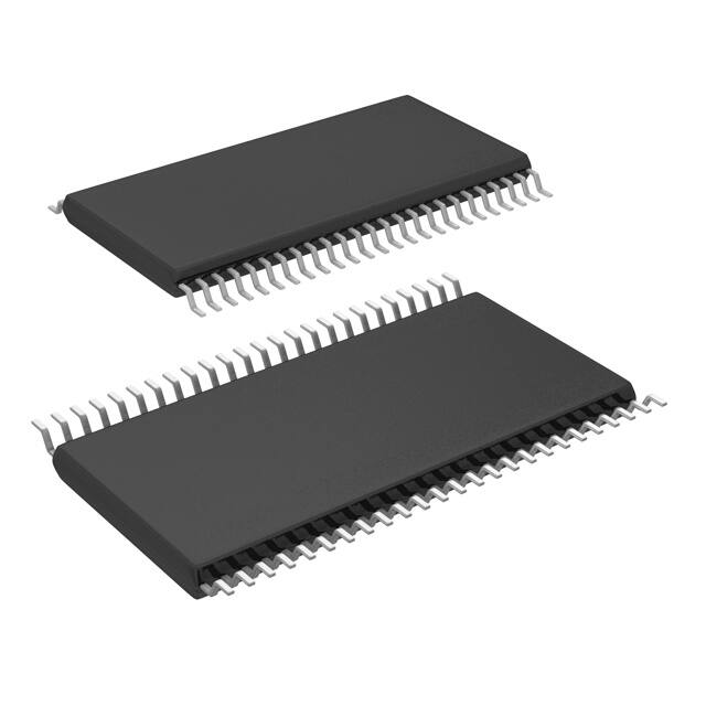
Packaged in a 48-Pin TSSOP Package
description
The CDC950 is a differential clock synthesizer/
driver that generates HCLK/HCLK, CLK33, 3V48,
and REFCLK system clock signals to support a
computer system with next generation processors
and double data rate (DDR) memory subsystems.
DGG PACKAGE
(TOP VIEW)
CLK33
VDD3.3V
3V48/SelA
3V48/SelB
GND
VDD3.3V
HCLK(0)
HCLK(0)
GND
HCLK(1)
HCLK(1)
VDD3.3V
HCLK(2)
HCLK(2)
GND
HCLK(3)
HCLK(3)
VDD3.3V
REFCLK
SPREAD
GND
XIN
XOUT
VDD3.3V
1
48
2
47
3
46
4
45
5
44
6
43
7
42
8
41
9
40
10
39
11
38
12
37
13
36
14
35
15
34
16
33
17
32
18
31
19
30
20
29
21
28
22
27
23
26
24
25
SEL100/133
GND
AVDD3.3V
AGND
PWRDWN
VDD3.3V
HCLK(4)
HCLK(4)
GND
HCLK(5)
HCLK(5)
VDD3.3V
HCLK(6)
HCLK(6)
GND
HCLK(7)
HCLK(7)
VDD3.3V
MultSel0
MultSel1
GND
AGND
I_REF
AVDD3.3V
All output frequencies are generated from a
14.318-MHz crystal input. A reference clock input
can be provided at the XIN input instead of a crystal. Two phase-locked loops (PLLs) are used to generate the
host frequencies and the 48-MHz clock frequencies. On-chip loop filters and internal feedback eliminate the
need for external components.
The HCLK, CLK33 clock, and 48-MHz clock outputs provide low-skew/low-jitter clock signals for reliable clock
operation. All outputs have 3-state capability, which can be selected through control inputs SEL100/133,
3V48/SelA, and 3V48/SelB.
The outputs are either differential host clock or 3.3-V single-ended CMOS buffers. With a logic high-level on the
PWRDWN terminal, the device operates normally. When a logical low-level input is applied, the device powers
down completely with the HOST clock at 2 × IREF, HOSTB is undriven, CLK33, 3V48, and REFCLK outputs are
in a low-level output state and 3V48B is in a high-level output state.
The host bus can operate at 100 MHz or 133 MHz. Output frequency selection is done with the corresponding
setting for SEL100/133 control input. The CLK33 (PCI) frequency is fixed to 33 MHz.
Since the CDC950 is based on PLL circuitry, it requires a stabilization time to achieve phase-lock of the PLL.
This stabilization time is required following power up, as well as following changes to the SEL inputs. With the
use of an external reference clock, this signal must be fixed-frequency and fixed-phase prior to stabilization time
starts. The CDC950 is characterized for operation from 0°C to 85°C.
Please be aware that an important notice concerning availability, standard warranty, and use in critical applications of
Texas Instruments semiconductor products and disclaimers thereto appears at the end of this data sheet.
Copyright 2001 − 2003, Texas Instruments Incorporated
���������� ���� ��!"#$%&�"� �' ()##*�& %' "! +),-�(%&�"� .%&*/
�#".)(&' ("�!"#$ &" '+*(�!�(%&�"�' +*# &0* &*#$' "! �*1%' ��'&#)$*�&'
'&%�.%#. 2%##%�&3/ �#".)(&�"� +#"(*''��4 ."*' �"& �*(*''%#�-3 ��(-).*
&*'&��4 "! %-- +%#%$*&*#'/
POST OFFICE BOX 655303
• DALLAS, TEXAS 75265
1
�������
����
� ��
�������� ����� ����
�������������
��
�� ��
����������������
SCAS646B − FEBRUARY 2001 − REVISED OCTOBER 2003
functional block diagram
3-State/Low
SEL100/133
48
Control
Logic
Test
SEL100/133
2
3V48/SelB
XIN
XOUT
1 REFCLK
14.318 MHz
(19)
4
Latched
22
23
48-MHz
PLL
Xtal
Oscillator
1 3V48
48 MHz
(3)
180°
Phase
Shift
/3
SPREAD
20
Spread
Logic
CPU
PLL
/2
/2
PWRDWN
MultSel0
MultSel1
I_REF
2
/2
44
1 CLK33
33.3 MHz
(1)
8 HCLKs
100/133 MHz
(7,10,13,16,
33,36,39,42)
30
29 Control Logic
1 3V48B
48 MHz
(4)
Sync Logic & Power Down Logic
3V48/SelA
3
2
8 HCLKs
100/133 MHz
(8,11,14,17
32,35,38,41)
26
POST OFFICE BOX 655303
• DALLAS, TEXAS 75265
�������
����
� ��
�������� ����� ����
�������������
��
�� ��
����������������
SCAS646B − FEBRUARY 2001 − REVISED OCTOBER 2003
Terminal Functions
TERMINAL
I/O
DESCRIPTION
NAME
NO.
3V48/SelA,
3V48/SelB
3, 4
I/O
AGND
27, 45
P
Analog ground
AVDD3.3V
CLK33
25, 46
P
Power. Analog power supply
1
O
33-MHz reference clock for PCI use, host clock divided by 3 or by 4
GND
5, 9, 15,
21, 28, 34,
40, 47
P
Ground
HCLK
7, 10, 13,
16, 33, 36,
39, 42
O
CPU and host clock outputs [7:0]. These eight differential CPU clock pairs run at 100/133 MHz. The VOH
swing amplitude is configured by MultSel0, MultSel1 pins. See Table 5 and Intel’s CK00 document for
details.
8, 11, 14,
17, 32, 35,
38, 41
O
CPU and host clock outputs [7:0]. These eight differential CPU clock pairs run at 100/133 MHz. The VOH
swing amplitude is configured by MultSel0, MultSel1 pins. See Table 5 and Intel’s CK00 document for
details.
I_REF
26
I
Current reference. This pin establishes the reference current for host clock parts. See Table 5 and Intel’s
CK00 document for details.
MultSel0
30
I
See Table 5 and Intel’s CK00 document for details.
MultSel1
29
I
See Table 5 and Intel’s CK00 document for details.
PWRDWN
44
I
Power-down input. 3.3-V LVTTL compatible, asynchronous input that requests the device to enter the
power-down mode. See Table 2 for details.
REFCLK
19
O
14.138-MHz reference clock output: 3.3 V copy of the 14.318-MHz reference clock.
SEL100/133
48
I
Active low LVTTL level logic select. SEL100/133 is used for enabling 100/133 MHz. Low = 100 MHz, high
= 133 MHz
SPREAD
20
U
Spread spectrum enable. 3.3-V LVTTL compatible, input that enables the spread spectrum mode when
held low. See Table 4 for details.
VDD3.3V
2, 6, 12,
18, 24, 31,
37, 43
P
Power. Power supply
XIN
22
I
Crystal connection or an external reference frequency input. Connect to either a 14.138-MHz crystal or
an external reference signal.
XOUT
23
O
Crystal connection. An output connection for an external 14.318-MHz crystal. If using an external
reference, this pin must be left unconnected.
HCLK
48-MHz 180° shifted pair clocks for USB use
Logic select pins. Selects the mode of operation, see Table 1 for details.
POST OFFICE BOX 655303
• DALLAS, TEXAS 75265
3
�������
����
� ��
�������� ����� ����
�������������
��
�� ��
����������������
SCAS646B − FEBRUARY 2001 − REVISED OCTOBER 2003
Function Tables
Table 1. Select Functions
INPUTS
OUTPUTS
FUNCTION
SEL100/133
SelA
SelB
HCLK, HCLK
CLK33
3V48, 3V48
REFCLK
0
0
0
100 MHz
33 MHz
48 MHz
14.318 MHz
Active 100 MHz
0
0
1
100 MHz
33 MHz
L, H
14.318 MHz
100 MHz mode; PLL48 powerdown
0
1
0
105 MHz
35 MHz
48 MHz
14.318 MHz
100 MHz mode 5% overclocking
0
1
1
Hi-Z
Hi-Z
Hi-Z
Hi-Z
1
0
0
133 MHz
33 MHz
48 MHz
14.318 MHz
Active 133 MHz
1
0
1
127 MHz
31.7 MHz
48 MHz
14.318 MHz
133 MHz mode −5% underclocking
1
1
0
133 MHz
33 MHz
48 MHz
14.318 MHz
Test mode
1
1
1
TCLK/2
TCLK/8
TCLK/2
TCLK
All 3-state outputs
Test mode (PLL bypass)
Table 2. Enable Functions
INPUT
OUTPUTS
PWRDWN
HCLK
HCLK
CLK33
3V48
3V48
REFCLK
0
2 × IREF
Hi-Z
L
L
H
L
1
On
On
On
On
On
On
Table 3. Output Buffer Specifications
BUFFER NAME
VDD RANGE
(V)
IMPEDANCE
(Ω)
BUFFER TYPE
3V48, REFCLK
3.135 − 3.465
20−60
TYPE 3
CLK33
3.135 − 3.465
12−55
TYPE 5
HCLK/HCLK
3.135 − 3.465
TYPE X1
Table 4. Spread Spectrum Functions
INPUT
OUTPUTS
SPREAD
4
0
Spread spectrum clocking active, −0.6% at HCLK/HCLK, CLK33
1
Spread spectrum clocking inactive
POST OFFICE BOX 655303
• DALLAS, TEXAS 75265
�������
����
� ��
�������� ����� ����
�������������
��
�� ��
����������������
SCAS646B − FEBRUARY 2001 − REVISED OCTOBER 2003
Function Tables (Continued)
Table 5. Host/HOST Output Buffer Specifications
INPUT
MultSel0
MultSel1
BOARD TARGET
TRACE/TERM Z
REFERENCE R,
IREF = VDD/(3 Rr)
OUTPUT CURRENT
IOH
VOH at Z
0
0
60 Ω
Rr = 475 1%,
I_REF = 2.32 mA
5 × IREF
0.71 V at 60 Ω
0
0
50 Ω
0
1
60 Ω
Rr = 475 1%,
I_REF = 2.32 mA
5 × IREF
0.59 V at 50 Ω
Rr = 475 1%,
I_REF = 2.32 mA
6 × IREF
0
1
0.85 V at 60 Ω
50 Ω
Rr = 475 1%,
I_REF = 2.32 mA
6 × IREF
0.71 V at 50 Ω
1
1
0
60 Ω
Rr = 475 1%,
I_REF = 2.32 mA
4 × IREF
0.56 V at 60 Ω
0
50 Ω
Rr = 475 1%,
I_REF = 2.32 mA
4 × IREF
0.47 V at 50 Ω
1
1
60 Ω
Rr = 475 1%,
I_REF = 2.32 mA
7 × IREF
0.99 V at 60 Ω
1
1
50 Ω
Rr = 475 1%,
I_REF = 2.32 mA
7 × IREF
0.82 V at 50 Ω
0
0
30 (dc equivalent)
Rr = 221 1%,
I_REF = 5 mA
5 × IREF
0.75 V at 30 Ω
0
0
25 (dc equivalent)
Rr = 221 1%,
I_REF = 5 mA
5 × IREF
0.62 V at 25 Ω
0
1
30 (dc equivalent)
Rr = 221 1%,
I_REF = 5 mA
6 × IREF
0.90 V at 30 Ω
0
1
25 (dc equivalent)
Rr = 221 1%,
I_REF = 5 mA
6 × IREF
0.75 V at 25 Ω
1
0
30 (dc equivalent)
Rr = 221 1%,
I_REF = 5 mA
4 × IREF
0.60 V at 30 Ω
1
0
25 (dc equivalent)
Rr = 221 1%,
I_REF = 5 mA
4 × IREF
0.5 V at 25 Ω
1
1
30 (dc equivalent)
Rr = 221 1%,
I_REF = 5 mA
7 × IREF
1.05 V at 30 Ω
1
1
25 (dc equivalent)
Rr = 221 1%,
I_REF = 5 mA
7 × IREF
0.84 V at 25 Ω
NOTE: The entries in boldface are the primary system configurations of interest. The outputs should be optimized for these configurations.
absolute maximum ratings over operating free-air temperature (unless otherwise noted)†
Supply voltage range, VDD . . . . . . . . . . . . . . . . . . . . . . . . . . . . . . . . . . . . . . . . . . . . . . . . . . . . . . . . . −0.5 V to 4.3 V
Input voltage range, VI (see Note 1) . . . . . . . . . . . . . . . . . . . . . . . . . . . . . . . . . . . . . . . . . . . –0.5 V to VDD + 0.5 V
Voltage range applied to any output in the high-impedance or power-off state, VO
(see Note 1) . . . . . . . . . . . . . . . . . . . . . . . . . . . . . . . . . . . . . . . . . . . . . . . . . . . . . . . . . . . –0.5 V to VDD + 0.5 V
Current into any output in the low state, IO . . . . . . . . . . . . . . . . . . . . . . . . . . . . . . . . . . . . . . . . . . . . . 2 × rated IOL
Input clamp current, IIK: (VI < 0) . . . . . . . . . . . . . . . . . . . . . . . . . . . . . . . . . . . . . . . . . . . . . . . . . . . . . . . . . . . –50 mA
(VI > VDD) . . . . . . . . . . . . . . . . . . . . . . . . . . . . . . . . . . . . . . . . . . . . . . . . . . . . . . . . . 50 mA
Output clamp current, IOK: (VO < 0) . . . . . . . . . . . . . . . . . . . . . . . . . . . . . . . . . . . . . . . . . . . . . . . . . . . . . . . –50 mA
VO > VDD) . . . . . . . . . . . . . . . . . . . . . . . . . . . . . . . . . . . . . . . . . . . . . . . . . . . . . . 50 mA
Package thermal impedance, θJA (see Note 2) . . . . . . . . . . . . . . . . . . . . . . . . . . . . . . . . . . . . . . . . . . . . . 89°C/W
Maximum power dissipation at TA = 55°C (in still air) (see Note 3) . . . . . . . . . . . . . . . . . . . . . . . . . . . 1070 mW
Operating free-air temperature range, TA . . . . . . . . . . . . . . . . . . . . . . . . . . . . . . . . . . . . . . . . . . . . . –0°C to 85°C
Storage temperature range, Tstg . . . . . . . . . . . . . . . . . . . . . . . . . . . . . . . . . . . . . . . . . . . . . . . . . . . –65°C to 150°C
Lead temperature 1,6 mm (1/16 inch) from case for 10 seconds . . . . . . . . . . . . . . . . . . . . . . . . . . . . . . . 260°C
† Stresses beyond those listed under “absolute maximum ratings” may cause permanent damage to the device. These are stress ratings only, and
functional operation of the device at these or any other conditions beyond those indicated under “recommended operating conditions” is not
implied. Exposure to absolute-maximum-rated conditions for extended periods may affect device reliability.
NOTES: 1. The input and output negative-voltage ratings may be exceeded if the input and output clamp-current ratings are observed.
2. The package thermal impedance is calculated in accordance with EIA/JEDEC Std JESD51, except for the through-hole packages,
which use a trace length of zero.
3. The maximum package power dissipation is calculated using a junction temperature of 150°C and a board trace length of 750 mils.
For more information, refer to the Package Thermal Considerations application note in the ABT Advanced BiCMOS Technology Data
Book, literature number SCBD002.
POST OFFICE BOX 655303
• DALLAS, TEXAS 75265
5
�������
����
� ��
�������� ����� ����
�������������
��
�� ��
����������������
SCAS646B − FEBRUARY 2001 − REVISED OCTOBER 2003
PACKAGE
DISSIPATION RATING TABLE
TA ≤ 25°C
DERATING FACTOR†
TA = 70°C
POWER RATING
POWER RATING
ABOVE TA = 25°C
TA = 85°C
POWER RATING
DGG
1400 mW
11.2 mW/°C
900 mW
730 mW
† This is the inverse of the traditional junction-to-case thermal resistance (RθJA) and uses a
board-mounted device at 89°C/W
recommended operating conditions (see Note 4)
Supply voltages, VDD, AVDD
High-level input voltage, VIH
MIN
NOM‡
MAX
3.135
3.3
3.465
2
Low-level input voltage, VIL
0.8
Input voltage, VI
−0.3
CLK33
−18
3V48/SelA and 3V48/SelB
−14
REFCLK
−14
HCLK/HCLK
0
CLK33
Low-level output current, IOL
Reference frequency, f(XIN)
Crystal, f(XTAL)¶
§
V
VDD + 0.3
−40
HCLK/HCLK
High-level output current, IOH
UNIT
mA
12
3V48/SelA and 3V48/SelB
9
REFCLK
9
Test mode
14
Normal mode
13.8
14.318
14.8
MHz
Operating free-air temperature, TA
0
85
°C
‡ All nominal values are measured at their respective nominal VDD values.
§ Reference frequency is a test clock driven on the XIN input during the device test mode or normal mode. In test mode, XIN can be driven externally
up to f(XIN) = 16 MHz. If XIN is driven externally, XOUT is floating.
¶ This is a series fundamental crystal with fo = 14.31818 MHz
NOTE 4: Unused inputs must be held high or low to prevent them from floating.
6
POST OFFICE BOX 655303
• DALLAS, TEXAS 75265
�������
����
� ��
�������� ����� ����
�������������
��
�� ��
����������������
SCAS646B − FEBRUARY 2001 − REVISED OCTOBER 2003
electrical characteristics over recommended operating free-air temperature range (unless
otherwise noted)
PARAMETER
TEST CONDITIONS
TYP†
MAX
UNIT
−1.2
V
VI = VDD
5
µA
VDD = 3.465 V,
VI = GND
−5
µA
VDD = 3.465 V
3V48/SelA, 3V48/SelB = H,
SEL100/133 = L,
VO = VDD or GND,
PWRDWN = H
±10
µA
High-impedance-state supply current‡
VDD = 3.465 V
3V48/SelA, 3V48/SelB = H,
SEL100/133 = L,
PWRDWN = H
19
25
mA
VDD Supply
43
47
mA
AIDD(PD)
PWRDWN state supply current‡
SelA, SelB = L
R(ref) = 475 Ω
PWRDWN = L
AVDD Supply
3.4
4.2
mA
Dynamic supply current‡
VDD = 3.465 V,
Rref = 475 Ω
Ω,
IO = 6 x Iref
PWRDWN = H
SSC = ON/OFF
CL = MAX
100 MHz
173
190
IDD(D)
133 MHz
183
200
VIK
Input clamp voltage
VDD = 3.135 V,
II = –18 mA
IIH
High-level input
current
All inputs except
SelA, SelB
VDD = 3.465 V,
IIL
Low-level input
current
All inputs except
SelA, SelB
IOZ
High-impedance
-state output
current
All outputs including
SelA, SelB
IDD(Z)
IDD(PD)
AlDD
Analog power supply current
CI
Input capacitance§
VDD = 3.465 V
MIN
mA
100 MHz and SSC off
19
24
133 MHz and SSC off
26
33
100 MHz and SSC on
26
33
133 MHz and SSC on
35
45
VDD = 3.3 V,
VI = VDD or GND
C(XTAL)
Crystal load capacitanceW
Effective capacity between CIN and COUT
† All typical values are measured at their respective nominal VDD values.
‡ CL = MAX = 5 pF, RS = 33.2 Ω, Rp = 49.9 Ω at HCLK/HCLK (Type X1)
CL = MAX = 20 pF, RL = 500 Ω at 48 MHz, REF (Type 3)
CL = MAX = 30 pF, RL = 500 Ω at CLK33 (Type 5)
§ These parameters are assured by design and lab characterization, not 100% production tested.
¶ This is the corresponding capacitive load for the XTAL in this oscillator application (Pierce oscillator)
POST OFFICE BOX 655303
• DALLAS, TEXAS 75265
2
5
13.5
22.5
mA
pF
7
�������
����
� ��
�������� ����� ����
�������������
��
�� ��
����������������
SCAS646B − FEBRUARY 2001 − REVISED OCTOBER 2003
electrical characteristics over recommended operating free-air temperature range (unless
otherwise noted) (continued)
HCLK/HCLK (Type X1)
PARAMETER
ro
Output resistance
VO
Output voltage
TEST CONDITIONS
MIN
Output current
All combinations of Table 5, See Note 5
Output capacitance
VDD = 3.30 V nom
NOTE 5: I(NOM) is output current (IOH) of table 5.
−7%
l(NOM)
7%
l(NOM)
−12%
l(NOM)
12%
l(NOM)
VO = VDD GND
UNIT
Ω
1.2
VDD = 3.30 V, ±5%
CO
MAX
3000
VDD = 3.30 V nom
IO
TYP†
3.5
V
mA
pF
3V48, 3V48REFCLK (Type 3)
PARAMETER
VOH
VOL
IOH
IOL
CO
High-level output voltage
Low-level output voltage
High-level output current
VDD = min to max,
VDD = 3.135 V,
VDD = min to max,
VDD = 3.135 V,
VDD = 3.135 V,
VDD = 3.3 V,
VDD = 3.465 V,
Low-level output current
VDD = 3.135 V,
VDD = 3.3 V,
Output capacitance
VDD = 3.465 V,
VDD = 3.3 V,
High state
Zo
TEST CONDITIONS
Output impedance
Low state
VO = 0.5 VDD,
VO = 0.5 VDD,
IOH = –1 mA
IOH = −14 mA
VO = 1 V
VO = 1.65 V
VO = 3.135 V
VO = 1.95 V
POST OFFICE BOX 655303
TYP†
MAX
0.1
0.18
V
0.4
−29
−37
−11
−23
mA
29
VO = 1.65 V
VO = 0.4 V
39
16
27
VO = VDD or GND
VO/IOH
4.5
20
40
60
VO/IOL
20
40
60
• DALLAS, TEXAS 75265
UNIT
VDD – 0.1
2.4
IOL = 1 mA
IOL = 9 mA
† All typical values are measured at their respective nominal VDD values.
8
MIN
7
pF
Ω
�������
����
� ��
�������� ����� ����
�������������
��
�� ��
����������������
SCAS646B − FEBRUARY 2001 − REVISED OCTOBER 2003
electrical characteristics over recommended operating free-air temperature range (unless
otherwise noted) (continued)
CLK33 (Type 5)
PARAMETER
TEST CONDITIONS
VOH
High-level output voltage
VDD = min to max,
VDD = 3.135 V,
IOH = –1 mA
IOH = −18 mA
VOL
Low-level output voltage
VDD = min to max,
VDD = 3.135 V,
IOL = 1 mA
IOL = 12 mA
VDD = 3.135 V,
VDD = 3.3 V,
VO = 1 V
VO = 1.65 V
VDD = 3.465 V,
VDD = 3.135 V,
VO = 3.135 V
VO = 1.95 V
IOH
High-level output current
MIN
TYP†
MAX
VDD – 0.1
2.4
0.1
0.15
0.4
−53
−16
−33
mA
30
Low-level output current
VDD = 3.3 V,
VDD = 3.465 V,
VO = 1.65 V
VO = 0.4 V
CO
Output capacitance
Output impedance
VO = VDD or GND
VO/IOH
4.5
Zo
VDD = 3.3 V,
VO = 0.5 VDD,
12
35
55
VO/IOL
12
35
55
Low state
VO = 0.5 VDD,
† All typical values are measured at their respective nominal VDD values.
V
−33
IOL
High state
UNIT
51
21
38
7.5
pF
Ω
switching characteristics, VDD = 3.135 V to 3.465 V, TA = 0°C to 85°C
PARAMETER
FROM
(INPUT)
TO
(OUTPUT)
TEST CONDITIONS
MIN
TYP
MAX
UNIT
VOH + 200
VOL − 200
mV
V(over)
V(under)
Overshoot†
Undershoot†
HCLK/HCLK 0.7-V
amplitude
V(over)
V(under)
Overshoot†
Undershoot†
Other clocks,
CL = worst case
tPZL
Output enable time
from low level
SEL100/133
All outputs
SEL100/133 ↑
Rref = 475 Ω
10
tPZH
Output enable time to
high level
SEL100/133
All outputs
SEL100/133 ↑
Rref = 475 Ω
10
tPHZ
Output disable time
from high level
SEL100/133
All outputs
SEL100/133 ↓
Rref = 475 Ω
10
tPLZ
Output disable time
from low level
SEL100/133
All outputs
Stabilization time‡
VDD
All outputs
ts
SEL100/133 ↓
Rref = 475 Ω
After power up
GND − 0.7
VDD + 0.7
V
ns
10
0.1
ms
PWRDWN
All outputs
From PWRDWN ↑
0.25
ms
† These parameters are assured by design and lab characterization, not 100% production tested.
‡ Stabilization time is the time required for the integrated PLL circuit to obtain phase lock of its feedback signal to its reference signal. In order for
phase lock to be obtained, a fixed-frequency, fixed-phase reference signal must be present at XIN. Until phase lock is obtained, the specifications
for propagation delay and skew parameters given in the switching characteristics tables are not applicable. Stabilization time is defined as the
time since VDD achieves its nominal operating level (3.3 V) or PWRDWN transition from a low to a high level (2 V) until the output frequency is
stable and operating within specification.
POST OFFICE BOX 655303
• DALLAS, TEXAS 75265
9
�������
����
� ��
�������� ����� ����
�������������
��
�� ��
����������������
SCAS646B − FEBRUARY 2001 − REVISED OCTOBER 2003
switching characteristics, VDD = 3.135 V to 3.465 V, TA = 0°C to 85°C (continued)
HCLK/HCLK (Type X1), CL = 2 pF, Rref = 475 Ω, 6 x Rref
PARAMETER
TEST CONDITIONS
HCLK clock period‡
f(HCLK) = 100 MHz
f(HCLK) = 133 MHz
Tjit(cc)
Cycle-to-cycle jitter
f(HCLK) = 100 or 133 MHz
tdc
Duty cycle
f(HCLK) = 100 or 133 MHz,
Crossing point
tsk(o)
HCLK bus skew
f(HCLK) = 100 or 133 MHz,
Crossing point
tr
tf
Rise time†
Fall time†
0.7-V amplitude
VO = 0.14 V to 0.56 V
VO = 0.14 V to 0.56 V
v(cross)
Cross point voltages†
0.7-V amplitude
f(HCLK) = 100 or 133-MHz
HCLK and HCLK
MIN
TYP
MAX
10
10.2
7.5
7.65
SSC off
−80
80
SSC on
−110
110
45%
55%
70
UNIT
ns
ps
ps
175
700
175
700
45%
VOH
55%
VOH
V
ps
† These parameters are assured by design and lab characterization, not 100% production tested.
‡ The average over any 1-µs period of time is greater than the minimum specified period.
CLK33 (Type 5), CL = 30 pF, RL = 500 Ω
PARAMETER
Tjit(cc)
t(dc)
PCI clock period†
Cycle-to-cycle jitter
Duty cycle
TEST CONDITIONS
MIN
TYP
MAX
UNIT
f(HCLK) = 100 or 133 MHz
30
30.06
30.6
ns
f(HCLK) = 100 or 133 MHz
f(CLK33) = 33.3 MHz
−150
150
ps
45%
55%
0.5
2
0.5
2
tr
Rise time
VO = 0.4 V to 2.4 V
tf
Fall time
VO = 0.4 V to 2.4 V
† The average over any 1-µs period of time is greater than the minimum specified period.
ns
3V48 (Type 3), CL = 20 pF, RL = 500 Ω
PARAMETER
TEST CONDITIONS
3V48 clock period
f(HCLK) = 100 or 133 MHz
Tjit(cc)
tdc
Cycle-to-cycle jitter
f(HCLK) = 100 or 133 MHz
f(3V48) = 48 MHz
tr
tf
Rise time
Duty cycle
Fall time
MIN
TYP
MAX
20.83
VO = 0.4 V to 2.4 V
VO = 0.4 V to 2.4 V
UNIT
ns
−300
300
45%
55%
1
4
1
4
ps
ns
REF (Type 3), CL = 20 pF, RL = 500 Ω
PARAMETER
REF clock period
TEST CONDITIONS
f(REF) = 14.318 MHz
f(HCLK) = 100 or 133 MHz
Tjit(cc)
t(dc)
Cycle-to-cycle jitter
tr
tf
Rise time
f(REF) = 14.318 MHz
VO = 0.4 V to 2.4 V
Fall time
VO = 0.4 V to 2.4 V
10
Duty cycle
POST OFFICE BOX 655303
MIN
TYP
MAX
69.84
• DALLAS, TEXAS 75265
−0.5
0.5
45%
55%
1
4
1
4
UNIT
ns
ns
�������
����
� ��
�������� ����� ����
�������������
��
�� ��
����������������
SCAS646B − FEBRUARY 2001 − REVISED OCTOBER 2003
PARAMETER MEASUREMENT INFORMATION
RL = 500 Ω
From Output
Under Test
VO(REF)
S1
tPLH/tPHL
tPLZ/tPZL
tPHZ/tPZH
GND
RL = 500 Ω
CL
(see Note A)
S1
TEST
OPEN
Open
VO(REF)
GND
LOAD CIRCUIT For tpd and tsk
tw
From Output
Under Test
3V
Test Point
VIH(REF)
VT(REF)
VIL(REF)
Input
CL
(see Note A)
0V
LOAD CIRCUIT for tr and tf
VOLTAGE WAVEFORMS
3V
Input
VT(REF)
VT(REF)
Output Enable
(High-Level
Enabling)
0V
tPLH
Output
tPHL
VOH
VIH(REF)
VT(REF)
VIL(REF)
VOL
tr
tw(high)
tf
Output
Waveform 1
S1 at 6 V
(see Note B)
Output
Waveform 2
S1 at GND
(see Note B)
tw(low)
VDD
VT(REF)
VT(REF)
0V
tPZL
tPLZ
≈3V
VT(REF)
VOL + 0.3 V
tPHZ
tPZH
VOL
VOH
VOH − 0.3 V
VT(REF)
≈0V
VOLTAGE WAVEFORMS
NOTES: A. CL includes probe and jig capacitance. CL = 2 pF (HCLK, HCLK), CL = 20 pF (48 MHz, REF), CL = 30 pF (CLK33).
B. Waveform 1 is for an output with internal conditions such that the output is low except when disabled by the output control.
Waveform 2 is for an output with internal conditions such that the output is high except when disabled by the output control.
C. All input pulses are supplied by generators having the following characteristics: PRR ≤ 14.318 MHz, ZO = 50 Ω, tr ≤ 2.5 ns, tf ≤ 2.5 ns.
D. The outputs are measured one at a time with one transition per measurement.
PARAMETER
3.3-V INTERFACE
VIH(REF)
High-level reference voltage
2.4
VIL(REF)
Low-level reference voltage
0.4
VT(REF)
Input threshold reference voltage
1.5
VO(REF)
Off-state reference voltage
UNIT
V
6
Figure 1. Load Circuit and Voltage Waveforms
POST OFFICE BOX 655303
• DALLAS, TEXAS 75265
11
�������
����
� ��
�������� ����� ����
�������������
��
�� ��
����������������
SCAS646B − FEBRUARY 2001 − REVISED OCTOBER 2003
APPLICATION INFORMATION
VDD
R(S1) = 33 Ω
HCLK
TLA
HCLK
MultSel0
CDC950
R(T1) = 49.9 Ω
MultSel1
R(S1) = 33 Ω
HCLK
TLB
HCLK
RI(REF) = 475 Ω
R(T1) = 49.9 Ω
CL = 2 pF
CL = 2 pF
CL Represents CBOARD and Cjig
ZTLA = ZTLB = 50 Ω
Figure 2. Load Circuit for HCLK Bus
spread spectrum clock (SSC) implementation for CDC950
Simultaneously switching at a fixed frequency generates a significant power peak at the selected frequency,
which in turn causes EMI disturbance to the environment. The purpose of the internal frequency modulation of
the CPU-PLL allows energy to be distributed to many different frequencies which reduces the power peak.
A typical characteristic for a single frequency spectrum and a frequency modulated spectrum is shown in
Figure 3.
∆
Maximum Peak
Non-SSC
SSC
δ of f(nom)
f(nom)
Figure 3. Frequency Power Spectrum With and Without the Use of SSC
The modulated spectrum has its distribution (left side) associated with the single-frequency spectrum which
indicates a down-spread modulation.
The peak reduction depends on the modulation scheme and modulation profile. System performance and timing
requirements are the limiting factors for actual design implementations. The implementation was driven to keep
the average clock frequency close to its upper specification limit. The modulation amount was set to
approximately –0.6%.
To allow a downstream PLL to follow the frequency modulated signal, the bandwidth of the modulation signal
is limited in order to minimize SSC induced tracking skew jitter. The modulation frequency is approximately
31 kHz.
12
POST OFFICE BOX 655303
• DALLAS, TEXAS 75265
�������
����
� ��
�������� ����� ����
�������������
��
�� ��
����������������
SCAS646B − FEBRUARY 2001 − REVISED OCTOBER 2003
MECHANICAL DATA
DGG (R-PDSO-G**)
PLASTIC SMALL-OUTLINE PACKAGE
48 PINS SHOWN
0,27
0,17
0,50
48
0,08 M
25
6,20
6,00
8,30
7,90
0,15 NOM
Gage Plane
1
0,25
24
0°−ā 8°
A
0,75
0,50
Seating Plane
0,15
0,05
1,20 MAX
PINS **
0,10
48
56
64
A MAX
12,60
14,10
17,10
A MIN
12,40
13,90
16,90
DIM
4040078 / F 12/97
NOTES: A.
B.
C.
D.
All linear dimensions are in millimeters.
This drawing is subject to change without notice.
Body dimensions do not include mold protrusion not to exceed 0,15.
Falls within JEDEC MO-153
POST OFFICE BOX 655303
• DALLAS, TEXAS 75265
13
�IMPORTANT NOTICE
Texas Instruments Incorporated and its subsidiaries (TI) reserve the right to make corrections, modifications,
enhancements, improvements, and other changes to its products and services at any time and to discontinue
any product or service without notice. Customers should obtain the latest relevant information before placing
orders and should verify that such information is current and complete. All products are sold subject to TI’s terms
and conditions of sale supplied at the time of order acknowledgment.
TI warrants performance of its hardware products to the specifications applicable at the time of sale in
accordance with TI’s standard warranty. Testing and other quality control techniques are used to the extent TI
deems necessary to support this warranty. Except where mandated by government requirements, testing of all
parameters of each product is not necessarily performed.
TI assumes no liability for applications assistance or customer product design. Customers are responsible for
their products and applications using TI components. To minimize the risks associated with customer products
and applications, customers should provide adequate design and operating safeguards.
TI does not warrant or represent that any license, either express or implied, is granted under any TI patent right,
copyright, mask work right, or other TI intellectual property right relating to any combination, machine, or process
in which TI products or services are used. Information published by TI regarding third-party products or services
does not constitute a license from TI to use such products or services or a warranty or endorsement thereof.
Use of such information may require a license from a third party under the patents or other intellectual property
of the third party, or a license from TI under the patents or other intellectual property of TI.
Reproduction of information in TI data books or data sheets is permissible only if reproduction is without
alteration and is accompanied by all associated warranties, conditions, limitations, and notices. Reproduction
of this information with alteration is an unfair and deceptive business practice. TI is not responsible or liable for
such altered documentation.
Resale of TI products or services with statements different from or beyond the parameters stated by TI for that
product or service voids all express and any implied warranties for the associated TI product or service and
is an unfair and deceptive business practice. TI is not responsible or liable for any such statements.
Following are URLs where you can obtain information on other Texas Instruments products and application
solutions:
Products
Amplifiers
Applications
amplifier.ti.com
Audio
www.ti.com/audio
Data Converters
dataconverter.ti.com
Automotive
www.ti.com/automotive
DSP
dsp.ti.com
Broadband
www.ti.com/broadband
Interface
interface.ti.com
Digital Control
www.ti.com/digitalcontrol
Logic
logic.ti.com
Military
www.ti.com/military
Power Mgmt
power.ti.com
Optical Networking
www.ti.com/opticalnetwork
Microcontrollers
microcontroller.ti.com
Security
www.ti.com/security
Telephony
www.ti.com/telephony
Video & Imaging
www.ti.com/video
Wireless
www.ti.com/wireless
Mailing Address:
Texas Instruments
Post Office Box 655303 Dallas, Texas 75265
Copyright 2003, Texas Instruments Incorporated
�


 工商网监
湘ICP备2023018690号
工商网监
湘ICP备2023018690号
