������
�����
��
�� ���� �������������
��� ������ �������� ���������� ��� ������ �
���
� ���������
SCAS675 – APRIL 2002
D Generates Clocks for AMD-K8 Clawhammer
D
D
D
D
D
D
D
D
Desktop Systems
Uses a 14.318-MHz Crystal Input to
Generate Multiple Output Frequencies
Includes Spread Spectrum Clocking (SSC),
0.5% Downspread for Reduced EMI
Power Management Control Terminals
SMBus Serial Interface Provides Output
Enable and Control
Low-Output Skew and Low Jitter for Clock
Distribution
Operates From Single 3.3-V Supply
Generates the Following Clocks:
– 2 CPU (3.3 V, 180° shifted pairs,
200/166/133/100 MHz)
– 6 PCI (3.3 V, 33 MHz)
– 1 PCI_F (3.3 V, 33 MHz)
– 3 REF (3.3 V, 14.318 MHz)
– 1 USB (3.3 V, 48 MHz)
– 1 FDC (3.3 V, 24 MHz or 48 MHz)
– 3 PCI/LDT† (3.3 V, 33 MHz or 66 MHz)
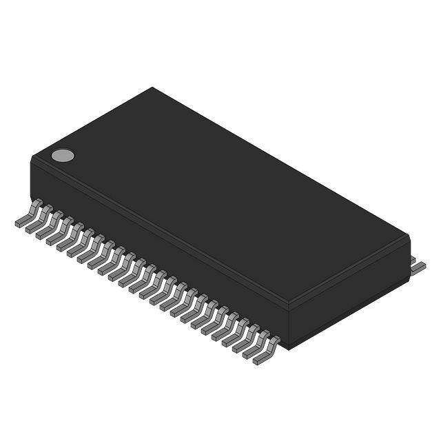
Packaged in 48-Pin SSOP Package
description
The CDC960 is a clock synthesizer/driver and
buffer that generates CPU, PCI, PCI/LDT, USB,
FDC, and REF system clock signals to support
PCs with an AMD-K8 Clawhammer-class system.
DL PACKAGE
(TOP VIEW)
FS0 & REF0
VDD
XIN
XOUT
GND
PCI/LDT_SEL
PCI/LDT0
PCI/LDT1
VDD
GND
PCI/LDT2
LDT_Stop
PCI0
PCI1
GND
VDD
PCI2
PCI3
VDD
GND
PCI4
PCI5
PCI_F
PCI_Stop
1
48
2
47
3
46
4
45
5
44
6
43
7
42
8
41
9
40
10
39
11
38
12
37
13
36
14
35
15
34
16
33
17
32
18
31
19
30
20
29
21
28
22
27
23
26
24
25
FS1 & REF1
GND
VDD
FS2 & REF2
SPREAD
VDDA
GNDA
CPU0
CPU0
GND
VDD
CPU1
CPU1
VDD
GND
GNDF
VDDF
USB
GND
VDD
24/48_SEL & FDC
GND
SDATA
SCLK
All output frequencies are generated from a 14.318-MHz crystal input. A reference clock input can be provided
at the XIN input instead of a crystal. It is recommended to use the bypass mode of the internal oscillator in this
case. Two phase-locked loops (PLLs) are used to generate the host frequencies and 48-MHz clock frequencies.
On-chip loop filters and internal feedback eliminate the need for external components.
The device provides a standard mode (100 kbps) SMBus 1.1 serial interface for device control. The
implementation is as a slave with read and write capability. The device address is specified in the SMBus serial
interface device address table. Both SMBus inputs (SDATA and SCLK) provide integrated pullup resistors
(typically 150 kΩ).
Seven 8-bit SMBus registers provide individual enable control for each of the outputs. The controllable outputs
default to enabled at power up and can be placed in a disabled mode with a low-level output when a low-level
control bit is written to the control register. The registers must be accessed in sequential order (i.e., random
access of the registers not supported).
The CPU, PCI, PCI_F, LDT, FDC (24/48-MHz), and USB (48-MHz) clock outputs provide low-skew/low-jitter
clock signals for reliable clock operation. All outputs have 3-state capability, which can be selected via control
inputs FS0, FS1, and FS2 at power-up preset condition.
Please be aware that an important notice concerning availability, standard warranty, and use in critical applications of
Texas Instruments semiconductor products and disclaimers thereto appears at the end of this data sheet.
†LDT is equivalent to HT66 shown on AMD specification.
Copyright 2002, Texas Instruments Incorporated
��
�����
� ���� � !"#$%&�" �' ()##* & %' "! +),-�(%&�" .%&*/
�#".)(&' (" !"#$ &" '+*(�!�(%&�" ' +*# &0* &*#$' "! �*1%' � '&#)$* &'
'&% .%#. 2%##% &3/ �#".)(&�" +#"(*''� 4 ."*' "& *(*''%#�-3 � (-).*
&*'&� 4 "! %-- +%#%$*&*#'/
POST OFFICE BOX 655303
• DALLAS, TEXAS 75265
1
�������
�����
��
�� ���� �������������
��� ������ �������� ���������� ��� ������ �
���
� ���������
SCAS675 – APRIL 2002
description (continued)
The CPU bus is a 3.3-V differential push-pull output type. All others are single-ended CMOS buffers.
The host frequencies are fixed and are controlled by the FS0, FS1 and FS2 signals at power-up. The CPU bus
frequencies are 200, 166, 133 and 100 MHz.
Because the CDC960 is based on PLL circuitry, it requires a stabilization time to achieve phase-lock of the PLL.
With use of external reference clock, this signal must be fixed-frequency and fixed-phase prior stabilization time
starts.
FUNCTION TABLES
DEVICE FREQUENCY SELECT FUNCTIONS
33 MHz
48 MHz
24 MHz
14.31818 MHz
33 MHz
66 MHz
48 MHz
24 MHz
14.31818 MHz
L
L
L
H
H
H
H
200 MHz
33 MHz
33 MHz
48 MHz
48 MHz
14.31818 MHz
L
L
L
L
H
H
H
200 MHz
33 MHz
66 MHz
48 MHz
48 MHz
14.31818 MHz
L
L
H/L
H/L
H
H
L
166 MHz
33 MHz
33/66 MHz
48 MHz
24/48 MHz
14.31818 MHz
L
L
H/L
H/L
H
L
H
133 MHz
33 MHz
33/66 MHz
48 MHz
24/48 MHz
14.31818 MHz
L
L
H/L
H/L
H
L
L
100 MHz
33 MHz
33/66 MHz
48 MHz
24/48 MHz
14.31818 MHz
L
L
X
H
L
L
H
Xin
Xin/6
Xin/6
L
L
L
L
L
X
L
L
L
H
Xin
Xin/6
Xin/3
L
L
L
L
L
H
H
L
H
H
Xin
Xin/6
Xin/6
Xin/2
Xin/4
Xin
L
L
H
L
L
H
H
Xin
Xin/6
Xin/3
Xin/2
Xin/4
Xin
L
L
L
H
L
H
H
Xin
Xin/6
Xin/6
Xin/2
Xin/2
Xin
L
L
L
L
L
H
H
Xin
Xin/6
Xin/3
Xin/2
Xin/2
Xin
L
L
X
X
L
H
L
L
L
X
X
L
L
L
L
H
H/L
H/L
H
H
L
H
H/L
H/L
H
H
L
H
H/L
H/L
H
L
H
H/L
H/L
H
L
H
H/L
H/L
L
H
H/L
H/L
L
H
H/L
H/L
L
H
H/L
H
X
H/L
FDC
USB †
FUNCTION
33 MHz
200 MHz
FSx and 24/48_SEL# pins
are latched at power up
200 MHz
H
f(xin) = 0 to
200 MHz
f(xin) = 0 to
16 MHz
Modes Test
H
H
PLL by-pass mode
H
H
REF †
CPU
H
L
†
FS0
H
H
PCI/LDT
FS1
H
L
PCI
‡
PCI/LDT_SEL
L
L
PCI_F
24/48_SEL‡
L
FS2
FS3 (Byte 0, Bit 4)
OUTPUTS
FS4 (Byte 0, Bit 5)
INPUTS
Comment
SMBUS
CONTROLLED
Reserved for future use
Hi-Z
Hi-Z
Hi-Z
Hi-Z
Hi-Z
Hi-Z
H
90 MHz
30 MHz
30/60 MHz
48 MHz
24/48 MHz
14.31818 MHz
–10%
L
119 MHz
30 MHz
30/60 MHz
48 MHz
24/48 MHz
14.31818 MHz
–10%
L
H
180 MHz
36.3 MHz
36.3/72.6 MHz
48 MHz
24/48 MHz
14.31818 MHz
–10%
L
L
180 MHz
30 MHz
30/60 MHz
48 MHz
24/48 MHz
14.31818 MHz
–10%
L
H
H
111 MHz
36.9 MHz
36.9/73.9 MHz
48 MHz
24/48 MHz
14.31818 MHz
10%
L
H
L
148 MHz
36.9 MHz
36.9/73.9 MHz
48 MHz
24/48 MHz
14.31818 MHz
10%
L
L
H
222 MHz
44.4 MHz
44.4/88.8 MHz
48 MHz
24/48 MHz
14.31818 MHz
10%
H/L
L
L
L
222 MHz
36.9 MHz
36.9/73.9 MHz
48 MHz
24/48 MHz
14.31818 MHz
10%
H/L
X
X
X
Not-yet-defined settings
† If the REF, USB, and FDC outputs are disabled in by pass mode, the Xin-input can be driven with an external clock signal from 0 MHz to 200 MHz.
Otherwise the maximum input frequency is limited to 16 MHz.
‡ 24/48_SEL and PCI/LDT_SEL inputs operate independently from each other and the frequency of the corresponding bus, as shown in detail
for the 200-MHz configuration.
2
POST OFFICE BOX 655303
• DALLAS, TEXAS 75265
�������
�����
��
�� ���� �������������
��� ������ �������� ���������� ��� ������ �
���
� ���������
SCAS675 – APRIL 2002
FUNCTION TABLES (Continued)
SPREAD SPECTRUM
INPUT
Spread
0
Spread spectrum disabled
1
Spread spectrum enabled, –0.5% at CPU/CPU, PCI/LDT, PCI_F, PCI
DEVICE ENABLE FUNCTIONS
SMBus
CONTROLLED
USB
FDC
REF
Hi-Z
Hi-Z
Hi-Z
Hi-Z
Hi-Z
Hi-Z
Hi-Z
Hi-Z
Off
Off
Xtal
↑↓
↑↓
↑↓
↑↓
↑↓
↑↓
↑↓
↑↓
↑↓
↑↓
L
X
X
H
H
L
H
X
X
X
Xtal
↑↓
↑↓
↑↓
L
L
↑↓
↑↓
↑↓
↑↓
↑↓
L
X
X
H
L
H
H
X
X
X
Xtal
↑↓
↑↓
↑↓
↑↓
↑↓
↑↓
↑↓
↑↓
↑↓
↑↓
L
X
X
H
L
L
H
X
X
X
Xtal
↑↓
↑↓
↑↓
L
L
↑↓
↑↓
↑↓
↑↓
↑↓
L
X
X
L
H
H
H
X
X
X
Xtal
↑↓
↑↓
↑↓
↑↓
↑↓
↑↓
↑↓
↑↓
↑↓
↑↓
L
X
X
L
H
L
H
X
X
X
Xtal
↑↓
↑↓
↑↓
L
↑↓
↑↓
↑↓
↑↓
↑↓
↑↓
L
X
X
L
L
H
H
X
X
X
Xtal
↑↓
↑↓
↑↓
↑↓
L
↑↓
↑↓
↑↓
↑↓
↑↓
L
X
X
L
L
L
H
X
X
X
Xtal
↑↓
↑↓
↑↓
L
L
↑↓
↑↓
↑↓
↑↓
↑↓
L
L
X
X
X
H
L
L
H
X
H
H
L
HL
HL
HL
L
L
L
Off
Off
L
L
X
H
X
H
L
L
H
X
L
L
H
HL
HL
HL
L
L
L
Off
Off
L
L
X
H
H
L
L
L
H
X
L
L
H
HL
L
L
L
L
L
Off
Off
L
L
X
L
L
H
L
L
H
X
H
H
L
HL
HL
L
L
L
L
Off
Off
L
L
X
L
H
L
L
L
H
X
L
L
H
HL
L
HL
L
L
L
Off
Off
L
L
X
H
H
L
L
H
X
X
H
H
L
HL
L
L
HL
HL
HL
Off
Off
L
L
X
H
H
L
L
H
X
X
L
L
H
HL
L
L
HL
HL
HL
Off
Off
L
L
X
H
L
H
L
H
X
X
H
H
L
HL
HL
HL
HL
HL
HL
Off
Off
L
L
X
H
L
H
L
H
X
X
L
L
H
HL
HL
HL
HL
HL
HL
Off
Off
L
L
X
L
H
L
L
H
X
X
L/H
L/H
H/L
HL
L
HL
HL
HL
HL
Off
Off
L
L
X
L
L
H
L
H
X
X
L/H
L/H
H/L
HL
HL
L
HL
HL
HL
Off
Off
L
L
X
L
L
L
L
H
X
X
L/H
L/H
H/L
HL
L
L
HL
HL
HL
Off
Off
PLL BYPASS MODE
‡
VCOs
PCI/LDT
Xtal
X
CRYSTAL
PCI
X
X
Comment
CPU
L
X
PCI_F
CPU
L
H
SPREAD
L
H
FS0
X
H
FS1
X
H
FS2
X
X
PCI_Stop
X
X
LDT_Stop
L
L
PCI/LDT_SEL
L
FS4 (Byte 0, Bit 5)
XIN
INTERNAL
24/48_SEL
OUTPUTS
FS3 (Byte 0, Bit 4)
INPUTS
† SMBus bits set to their reset values
‡ Hi-Z will have LOW state if external load circuit is applied, CPU and CPU are push-pull type outputs.
↑↓ Outputs toggle at the selected frequency according to the Device Frequency Select FunctionS table above.
HL device output state is undefined, either L or H. It is L if Xin is held static at L or H before the bypass mode is selected.
OUTPUT BUFFER SPECIFICATIONS
BUFFER NAME
VDD RANGE
(V)
IMPEDANCE
(Ω)
LUMPED TEST LOAD
CPU
3.135 – 3.465
40
10 pF
PCI, PCI_F, LDT
3.135 – 3.465
25
30 pF
REF, USB, FDC
3.135 – 3.465
35
20 pF
POST OFFICE BOX 655303
• DALLAS, TEXAS 75265
3
�������
�����
��
�� ���� �������������
��� ������ �������� ���������� ��� ������ �
���
� ���������
SCAS675 – APRIL 2002
functional block diagram
SMBus
44
150 kΩ
150 kΩ
Control
Logic
150 kΩ
SPREAD
25
26
150 kΩ
SCLK
SDATA
/2
VDD
VDD
1 x FDC
24/48 MHz
24/48_SEL
(28)
@ Power Up
1 x USB
48 MHz
(31)
XOUT
3
Xtal
Oscillator
4
CPU
PLL
/2
/2
SPREAD
SPECTRUM
LDT_Stop
12
/3
150 kΩ
VDD
/4
0
/5
/6
Sync and Power Up/Power Down Logic
XIN
150 kΩ
48 MHz
PLL
VDD
3 x REF
14.318 MHz
FS0, FS1, FS2
(1, 45, 48)
@ Power Up
2 x CPU
(200/166/133/100 MHz)
(37, 41)
2 x CPU
(200/166/133/100 MHz)
(36, 40)
1
PCI/LDT_SEL
PCI_Stop
6
150 kΩ
150 kΩ
VDD
3 x PCI/LDT
33/66 MHz
(7, 8, 11)
/2
24
6 x PCI
33 MHz
(13, 14, 17, 18, 21, 22)
1 x PCI_F
33 MHz
(23)
4
POST OFFICE BOX 655303
• DALLAS, TEXAS 75265
�������
�����
��
�� ���� �������������
��� ������ �������� ���������� ��� ������ �
���
� ���������
SCAS675 – APRIL 2002
Terminal Functions
TERMINAL
NAME
NO.
I/O
DESCRIPTION
CPU[0:1],CPU[0:1]
41, 37
40, 36
O
3.3-V, differential CPU clock outputs
CPU Clock Outputs 0 and 1: CPU push-pull true clock outputs of the differential pair
CPU Clock Outputs 0 and 1: CPU push-pull complementary clock outputs of the differential pair
FS[0:2] & REF[0:2]
1, 48, 45
I/O
3.3 V, 14.318-MHz clock outputs
Frequency Select inputs: Power–on strapping to set device operating frequency as described in
the Device Frequency Select Functions table. These inputs have 150-kΩ internal pullup resistors.
Low = 0, High = 1. 3.3-V reference clock outputs: Fixed clock output at 14.318 MHz
5, 10, 15,
20, 27, 30,
34, 39, 47
G
Power Connection: Connected to VSS. Used to ground digital portions of the chip
GNDA
42
G
Analog GND: Connected to VSS through filter. Used to ground the main CPU-PLL on the chip
GNDF
33
G
Analog GND for 48-MHz PLL: Connected to VSS through filter. Used to ground the 48-MHz PLL on
the chip
LDT_Stop
12
I
Control for 66-MHz PCI clocks: Active LOW control input to halt all 66-MHz PCI clocks except the
free-running clock. This input has a 150-kΩ internal pullup resistor. Once this input has been
asserted, PCI/LDT outputs if operating at 66-MHz must stop in the low state within 1 µs.
Low = stop, High = running
13, 14, 17,
18, 21, 22
O
3.3-V PCI clock outputs divided down from CPU-PLL
3.3-V PCI clock outputs: PCI clocks operate at 33 MHz.
23
O
3.3-V, 33-MHz clocks divided down from CPU-PLL
3.3-V Free-Running PCI clock output: The free-running PCI clock pin operates at 33 MHz. The
free-running PCI clock is not turned off when PCI_Stop# is activated LOW.
PCI/LDT[0:2]
7, 8, 11
O
3.3-V PCI 33-MHz or LDT 66-MHz outputs: This group of outputs is selectable between 33 MHz
and 66 MHz based upon the state of PCI/LDT_SEL. When running at 66 MHz these outputs are for
use as reference clocks to LDT devices.
PCI/LDT_SEL
6
I
PCI 33-MHz/LDT 66-MHz Select: This input selects the output frequency of PCI/LDT outputs to
either 33 MHz or 66 MHz. This is a dedicated input pin to avoid corruption of the input state due to
PCI add-in cards that may have termination resistors on the input clocks. This input has a 150-kΩ
internal pullup resistor. Low = 66-MHz outputs, High = 33-MHz outputs
PCI_Stop
24
I
3.3-V LVTTL-compatible input for PCI_Stop active low
Control for 33-MHz PCI clocks: Active LOW control input to halt all 33-MHz PCI clocks except the
free-running clock. This input has a 150-kΩ internal pullup resistor. Once this input has been
asserted, the PCI outputs and PCI/LDT outputs operating at 33 MHz must stop in the low state
within 1 µs.
Low = stop, High = running
SCLK
25
I
SMBus compatible SCLK.
Clock pin for SMBus circuitry (SMBus revision 1.1). This input has an internal pull-up resistor of
150 kΩ. SCLK is a 3.6-V tolerant signal input. High impedance at power down is not supported.
SDATA
26
I/O
SMBus compatible SDATA
Data pin for SMBus circuitry (SMBus revision 1.1). This output is open drain and has an internal
pullup resistor of 150 kΩ. SDATA is a 3.6V tolerant signal IO. High impedance at power down is not
supported.
SPREAD
44
I
Spread Spectrum Clocking Enable: Power-on strapping to set spread spectrum clocking as
enabled or disabled. This input allows the default spread spectrum clocking mode to be enabled or
disabled upon power up. This input has a 150-kΩ internal pullup resistor.
Low = disable, High = enable. Note that all Athlon and Hammer systems are recommended to use
SSC; therefore, the default of this pin is enabled and should only be turned off for debug and test
purposes.
USB
31
O
3.3-V, fixed 48-MHz non-SSC clock output
3.3-V USB clock output: Fixed clock output at 48 MHz
VDD
2, 9, 16,
19, 29, 35,
38, 46
P
Power Connection: Connected to 3.3-V power supply. Used to supply digital portions of the chip
GND
PCI[0:5]
PCI_F
POST OFFICE BOX 655303
• DALLAS, TEXAS 75265
5
�������
�����
��
�� ���� �������������
��� ������ �������� ���������� ��� ������ �
���
� ���������
SCAS675 – APRIL 2002
Terminal Functions (Continued)
TERMINAL
NAME
NO.
I/O
DESCRIPTION
VDDA
43
P
Analog VDD: Connected to 3.3-V power supply through filter. Used to supply the main CPU-PLL
on the chip
VDDF
32
P
Analog VDD for 48-MHz PLL: Connected to 3.3-V power supply through filter. Used to supply the
48-MHz PLL on the chip
XIN
3
I
Crystal input – 14.318 MHz
Crystal Connection or External Reference: Reference crystal input or external reference clock
input. This pin includes an internal 36-pF load capacitance to eliminate the need for an external
load capacitor.
XOUT
4
O
Crystal output – 14.318 MHz
Crystal Connection: Reference crystal feedback. This output includes an internal 36-pF load
capacitance to eliminate the need for an external load capacitor.
24/48_SEL & FDC
28
I/O
3.3-V super I/O clock output: The super I/O clock can be strapped for 24 MHz or 48 MHz. This
input has a 150-kΩ internal pullup resistor.
Low = 48-MHz output, High = 24-MHz output
connecting SCLK and SDATA to 5-V SMBus signals
SCLK and SDATA of CDC960 have been designed to work within a 3.3-V supply voltage environment only. In
order to connect SCLK and SDATA to a 5-V SMBus configuration, external circuitry is required. A simple and
inexpensive solution is to use clamping diodes. Two approaches are recommended for this solution:
1. Using Zener diode to clamp to GND in reverse-biased direction
3.3 V
SCLK
OR
SDATA
Driver
150 kΩ
VO
R1
VIO
D1
SCLK
or
SDATA
CDC960
Figure 1. SCLK SDATA Connection to 5-V SMBus Using Zener Diode
Zener diode D1 in Figure 1 is chosen such that the Zener voltage (VZK) cannot exceed 300 mV above VDD of
the CDC960. The minimum value of VZK must be greater than 2.1 V to meet minimum requirement for VIH of
the CDC960. The value of R1 is chosen to satisfy requirements both for IOH of the driver of SCLK and SDATA
and for VOL and IOL of SDATA of CDC960.
I
OH
v
V
O
IO
ǒR1 ) RSǓ
2 mA v
0.8 V
R1 ) Z
ǒR1 ) ZOǓ
6
*V
(For the driver of SCLK and SDATA. R S is the source driver impedance.)
v 6 mA
(1)
(For a SDATA of CDC960, 25 W t Z
O
O
1.75 mA t 0.4 V (For a SDATA of CDC960, 25 W t Z
POST OFFICE BOX 655303
• DALLAS, TEXAS 75265
t 47 W)
(2)
O
t 47 W)
(3)
�������
�����
��
�� ���� �������������
��� ������ �������� ���������� ��� ������ �
���
� ���������
SCAS675 – APRIL 2002
connecting SCLK and SDATA to 5-V SMBus signals (continued)
There are many manufacturers making Zener diodes that can be used for this application. Panasonic MA8033
and Vishay BZX84C3V3 that have 3.1 V < VZ < 3.5 V can be used for this application. In this case R1 is
recommended as 150 Ω.
The worst IOH in equation (1) is 16 mA when VOH = 5.5 V, RS = 0 Ω and VIO = 3.1 V.
The current in equation (2), between 4 mA and 4.6 mA, satisfies the requirement.
Equation (3) is also satisfied with the selected R1 and diode.
2. Clamping Diode to VDD
3.3 V
3.3 V
D1
SCLK
OR
SDATA
Driver
VO
R1
150 kΩ
VIO
SCLK
or
SDATA
CDC960
Figure 2. SCLK SDATA Connection to 5-V SMBus Using Clamping Diode to VDD
Diode D1 in Figure 2 should have a small forward voltage (VF). Ideally, we want VF to be less than 300 mV to
meet the input voltage requirement of the CDC960. International IOR Rectifier has a device (part number
10BQ015) with maximum VF of 350 mV at 1.0 A. Using the 10BQ015 with R1 = 150 Ω, the worst-case IOH is
calculated using equation (4).
I
OH
+
5.5 V * (3.0 * 0.35) V
+ 14 mA
150 W
(4)
The calculation for equations (2) and (3) is the same as in part 1.
When using the configuration in Figure 2, the power supply is required to have a capability of sinking current.
The total amount of sinking current is dependent on the overall load connected to that power supply.
Using the above interface circuitry with a high-impedance source, the available high-level voltage on the SMBus
is limited to about (Vzk) for the configuration in Figure 1 and (VDD(CDC960) + VF(D1)) for the configuration in
Figure 2. One has to choose which option best fits a given SMBus configuration.
Actually, the typical SMBus configuration is an open-drain configuration with pullup resistors to the
corresponding power supply. It does not require a 5-V SMBus driver that has a low impedance to drive the
CDC960 SMBus ports with its additional components as shown in Figure 1 and Figure 2. The external
components are not needed if the pullup resistors of the SMBus are directly connected to a voltage equal to
the supply voltage of the CDC960 (typically 3.3 V). This pullup resistor connection is strongly recommended.
POST OFFICE BOX 655303
• DALLAS, TEXAS 75265
7
�������
�����
��
�� ���� �������������
��� ������ �������� ���������� ��� ������ �
���
� ���������
SCAS675 – APRIL 2002
power-up sequences
Sampled inputs are: FS0, FS1, FS2 and 24/48_SEL.
State S1 is an analog controlled delay derived from internal reference voltages to ensure that a valid input state
is captured. There is no specific delay in this state after power up.
Figure 3 shows the symbolic sequence of the CDC960 during power up. States S0–S4 are required to ensure
proper configuration and operation of the device functions.
Outputs Disabled
S1
S2
Delay
Sample
Input Straps
VDD ≤ 2 V
Outputs
Undefined
S0
VDD = Off
Power Off
Enable
Outputs
S4
S3
Normal
Operation
Power Up
Wait
3 ms
Figure 3. Power-Up State Transitions
SMBus serial interface
The following section describes the SMBus interface programming.
In general the CDC960 SMBus protocol supports only block write and block read operations.
SMBus device address
A6
A5
A4
A3
A2
A1
A0
R/W
1
1
0
1
0
0
1
0
0 = write to CDC960
1 = read from CDC960
writing to the SMBus interface
1. Send the address D2(H) and validate the acknowledge from the slave.
2. Send the dummy byte as a command code and validate the acknowledge from the slave.
3. Send the number of data bytes to write and validate the acknowledge from the slave.
4. Write the desired data bytes to registers and validate the acknowledge from the slave for each data byte.
Clock Generator
Addr (7 bits)
A(6:0) & R/W
ACK
+8 bits dummy
command code
ACK
+8 bits byte
count
ACK
D2(H)
8
POST OFFICE BOX 655303
• DALLAS, TEXAS 75265
Data byte 0
ACK
Data byte N
ACK
�������
�����
��
�� ���� �������������
��� ������ �������� ���������� ��� ������ �
���
� ���������
SCAS675 – APRIL 2002
SMBus serial interface (continued)
reading the SMBus interface, using address pre-phase
1. Send the address D2(H) and validate the acknowledge from the slave.
2. Send dummy byte as command code and validate the acknowledge from the slave.
3. Send repeated start condition followed by address D3(H) and validate the acknowledge from the slave.
4. The slave returns the number of bytes it is going to send (byte count) and validates the acknowledge from
the master.
5. Read back the desired data bytes and validate the acknowledge sent by the master for each data byte.
Clock
Generator
Addr
(7 bits)
ACK
A(6:0)&
R/W
+8 bits
dummy
command
code
ACK
D2(H)
Re
eated
Repeated
Start
Clock
Generator
Addr
(7 bits)
ACK
A(6:0)&
R/W
+8 bit byte
count
ACK by
master
Data
byte 0
ACK by
master
Data
byte N
ACK by
master
D3(H)
reading the SMBus interface, using direct read
1. Send the address D3(H) and validate the acknowledge from the slave.
2. The slave returns the number of bytes it is going to send (byte count) and validates the acknowledge from
the master.
3. Read back the desired data bytes and validate the acknowledge sent by the master for each data byte.
Clock
Generator
Addr (7 bits)
A(6:0)& R/W
ACK
+8 bit byte
count
ACK by master
Data byte 0
ACK by master
Data byte N
ACK by master
D3(H)
POST OFFICE BOX 655303
• DALLAS, TEXAS 75265
9
�������
�����
��
�� ���� �������������
��� ������ �������� ���������� ��� ������ �
���
� ���������
SCAS675 – APRIL 2002
SMBus configuration command bitmap
Byte 0: Frequency and Spread Spectrum Control Register (see Note 1)
(H = Enable, L = Disable)
BIT
TYPE
PUD†
DESCRIPTION
PIN AFFECTED
(WRITE
OPERATION)
SOURCE PIN
(READ
OPERATION)
7
R/W
L
Write disable (write once). A 1 written to this bit after a 1 has been written to
Byte0, Bit0 disables modification of all configuration registers until the device has been powered off.
—
Register value
—
Register value
Spread spectrum enable. This bit provides a software programmable control forspread spectrum clocking. The truth table for SSC is as follows:
Spread (ext. Pin)
6
R/W
5
R/W
4
L
Byte0, Bit6
SSC Function
L
L
Disabled
L
H
Enabled
H
L
Enabled
H
H
Enabled
L
FS4 (corresponds to frequency selection table)
—
Register value
R/W
L
FS3 (corresponds to frequency selection table)
—
Register value
3
R/W
Externally
selected‡
FS2 (corresponds to frequency selection table). If write is enabled, this bit
can be set differently than the power-up condition.
—
45 at power up
2
R/W
Externally
selected‡
FS1 (corresponds to frequency selection table). If write is enabled, this bit
can be set differently than the power-up condition.
—
48 at power up
1
R/W
Externally
selected‡
FS0 (corresponds to frequency selection table). If write is enabled, this bit
can be set differently than the power-up condition.
—
1 at power up
L
Write Enable. A 1 written to this bit after power up enables modification of all
configuration registers and subsequent 0s written to this bit disable modification of all configuration registers except this single bit. Note that when a 1
has been written to Byte0, Bit 7, all modification is permanently disabled until the device power cycles. Note also, that block write transactions to the
interface are completed. However, unless the interface has been previously
unlocked, the writes have no effect.
—
Register value
0
R/W
† PUD = Power-up condition
‡ The value of this bit is according to level applied to corresponding device pin at power up.
NOTE 1: Byte0, Bit0 controls the write enable status for the device SMBus. If a 1 is written to Byte0, Bit0, the SMBus registers are write enabled.
Once write has been enabled, a new block write protocol must be sent to the device to program the desired register values. Once after
power up a 1 is written to Byte0, Bit0, the device functionality is according to the settings of the different registers. E.g., the device function
table is according to setting of Bits[1…6] of Byte0 and other functions are according to corresponding SMBus register settings.
If a 0 is written to Byte0, Bit0, write is disabled and the device function is according to the previous settings of the last write cycle.
Byte 1: PCI Clock Control Register
(H = Enable, L = Disable)
BIT
TYPE
PUD†
DESCRIPTION
PIN AFFECTED
(WRITE OPERATION)
SOURCE PIN
(READ OPERATION)
7
R/W
H
PCI/LDT1 enable
8
Register value
6
R/W
H
PCI/LDT0 enable
7
Register value
5
R/W
H
PCI5 enable
22
Register value
4
R/W
H
PCI4 enable
21
Register value
3
R/W
H
PCI3 enable
18
Register value
2
R/W
H
PCI2 enable
17
Register value
1
R/W
H
PCI1 enable
14
Register value
PCI0 enable
13
Register value
0
R/W
H
† PUD = Power-up condition
10
POST OFFICE BOX 655303
• DALLAS, TEXAS 75265
�������
�����
��
�� ���� �������������
��� ������ �������� ���������� ��� ������ �
���
� ���������
SCAS675 – APRIL 2002
SMBus configuration command bitmap (continued)
Byte 2: PCI Clock USB FDC and REF Control Register
(H = Enable, L = Disable)
BIT
TYPE
PUD†
DESCRIPTION
PIN AFFECTED
(WRITE OPERATION)
SOURCE PIN
(READ OPERATION)
7
R/W
H
CPU1 enable‡
36, 37
Register value
6
R/W
H
CPU0 enable‡
40, 41
Register value
5
R/W
H
REF2 enable
45
Register value
4
R/W
H
REF1 enable
48
Register value
3
R/W
H
REF0 enable
1
Register value
2
R/W
H
FDC (24_48 MHz) enable
28
Register value
1
R/W
H
USB enable
31
Register value
0
R/W
H
PCI/LDT2 enable
11
Register value
† PUD = Power-up condition
‡ If a CPU clock is disabled by setting its control bit (bit 6 or bit 7) low, both the CPU and CPU outputs for the disabled clock are set low.
Byte 3: PCI Clock Free Running Control Register
PIN AFFECTED
(WRITE OPERATION)
SOURCE PIN
(READ OPERATION)
PCI/LDT1 free-running enable§
PCI/LDT0 free-running enable§
8
Register value
7
Register value
PCI5 free-running enable§
PCI4 free-running enable§
22
Register value
21
Register value
PCI3 free-running enable§
PCI2 free-running enable§
18
Register value
17
Register value
PCI1 free-running enable§
PCI0 free-running enable§
14
Register value
BIT
TYPE
PUD†
DESCRIPTION
7
R/W
L
6
R/W
L
5
R/W
L
4
R/W
L
3
R/W
L
2
R/W
L
1
R/W
L
(H = Free running, L = controlled by PCI_Stop/LDT_Stop))
0
R/W
L
13
Register value
† PUD = Power-up condition
§ The above individual free-running enable/disable controls are intended to allow individual clock outputs to be made free running. A clock output
that has its free-running bit enabled (set to H) is not turned off with the assertion of either PCI_Stop or LDT_Stop. If a particular bit is disabled
in Byte1, the Byte1 settings overwrite the Byte3 settings.
POST OFFICE BOX 655303
• DALLAS, TEXAS 75265
11
�������
�����
��
�� ���� �������������
��� ������ �������� ���������� ��� ������ �
���
� ���������
SCAS675 – APRIL 2002
SMBus configuration command bitmap (continued)
Byte 4: Pin Latched/Real Time State Control Register (see Note 2)
(H = Enable, L = Disable)
PUD†
DESCRIPTION
PIN AFFECTED
(WRITE OPERATION)
SOURCE PIN
(READ OPERATION)
R/W
H
PCI_F enable
23
Register value
6
R
Externally
selected‡§
SPREAD actual pin state
44
5
R
Externally
selected‡
24/48_SEL pin power up latched state
28 at power up
4
R
Externally
selected‡§
PCI/LDT_SEL actual pin state
6
3
R
Externally
selected‡
FS2 power-up latched pin state
45 at power up
2
R
Externally
selected‡
FS1 power-up latched pin state
48 at power up
1
R
Externally
selected‡
FS0 power-up latched pin state
1 at power up
BIT
TYPE
7
0
R/W
L
PCI/LDT2 free-running enable¶
11
Register value
† PUD = Power-up condition
‡ The value of this bit is determined by the level applied to the corresponding device pin at power up.
§ If the SMBus is in read mode, and the byte-count byte is being sent, the device input pin is sampled again at the falling edge of SCLK at the same
state as the acknowledge state for the byte count that is initiated by SCLK↓.
¶ The above individual free running enable/disable controls are intended to allow individual clock outputs to be made free running. A clock output
that has its free-running bit enabled (set to H) is not turned off with the assertion of either PCI_Stop or LDT_Stop. If a particular bit is disabled
in Byte2, the Byte2 settings overwrite the Byte4 settings.
NOTE 2: Byte4 holds the power-up information for pins latched at power up. In the case that an unintentional write has been made to these bits
of Byte4, the SMBus write is ignored; the bits always return the power-up latched value during an SMBus read operation.
This does not relate to the bits which hold the actual (current) pin state. Those bits can not be overwritten by software in order to get
the hardware setting states back via software.
Byte 5: Vendor Identification Register
(H = Enable, L = Disable)
BIT
TYPE
PUD†
DESCRIPTION
PIN AFFECTED
(WRITE OPERATION)
7
R
H
Manufacturer ID (MSB)
–
Returns H
6
R
H
Manufacturer ID
–
Returns H
5
R
H
Manufacturer ID, TI is shown for vendor ID = 111
–
Returns H
4
R
L
Device revision ID (MSB)
–
Returns L
3
R
L
Device revision ID
–
Returns L
2
R
L
Device revision ID
–
Returns L
1
R
L
Device revision ID
–
Returns L
0
R
H
Device revision ID, device revision: 00001
–
Returns H
† PUD = Power-up condition
12
POST OFFICE BOX 655303
• DALLAS, TEXAS 75265
SOURCE PIN
(READ OPERATION)
�������
�����
��
�� ���� �������������
��� ������ �������� ���������� ��� ������ �
���
� ���������
SCAS675 – APRIL 2002
SMBus configuration command bitmap (continued)
Byte 6: Byte Count Control Register
(H = Enable, L = Disable)
BIT
TYPE
PUD†
DESCRIPTION
PIN AFFECTED
(WRITE OPERATION)
SOURCE PIN
(READ OPERATION)
7
R/W
L
Byte count bit, MSB
–
Register value
6
R/W
L
Byte count bit
–
Register value
5
R/W
L
Byte count bit
–
Register value
4
R/W
L
Byte count bit
–
Register value
3
R/W
L
Byte count bit
–
Register value
2
R/W
H
Byte count bit
–
Register value
1
R/W
H
Byte count bit
–
Register value
0
R/W
H
Byte count bit, LSB
–
Register value
† PUD = Power-up condition
Byte 7: Vendor Specific Register (reserved)
(H = Enable, L = Disable)
BIT
TYPE
PUD†
DESCRIPTION
PIN AFFECTED
(WRITE OPERATION)
SOURCE PIN
(READ OPERATION)
7
R/W
L
Must be set to L during the byte write
–
Register value
6
R/W
L
Must be set to L during the byte write
–
Register value
5
R/W
L
Must be set to L during the byte write
–
Register value
4
R/W
L
Must be set to L during the byte write
–
Register value
3
R/W
L
Must be set to L during the byte write
–
Register value
2
R/W
L
Must be set to L during the byte write
–
Register value
1
R
L
Must be set to L during the byte write
–
Register value
0
R
L
Must be set to L during the byte write
–
Register value
† PUD = Power-up condition
POST OFFICE BOX 655303
• DALLAS, TEXAS 75265
13
�������
�����
��
�� ���� �������������
��� ������ �������� ���������� ��� ������ �
���
� ���������
SCAS675 – APRIL 2002
SMBus configuration command bitmap (continued)
Byte 8: Vendor Specific Register (reserved)
BIT
TYPE
(H = Enable, L = Disable)
PUD†
DESCRIPTION
PIN AFFECTED
(WRITE OPERATION)
SOURCE PIN
(READ OPERATION)
CPU, CPU
Register value
7
R/W
L
Trigger single pulse at the L-to-H transition of this bit
after an SMBus write cycle completes. This bit must be
written back to L in order to trigger a following pulse with
a new L-to-H transition at the completion of a write
protocol.
6
R/W
L
Single-pulse ARM bit
H = enable, L = disable single-pulse feature
–
Register value
5
R/W
L
Must set to L during the byte write
–
Register value
4
R/W
L
Must set to L during the byte write
–
Register value
3
R/W
L
Must set to L during the byte write
–
Register value
2
R/W
L
Must set to L during the byte write
–
Register value
1
R/W
L
Must set to L during the byte write
–
Register value
0
R/W
L
Must set to L during the byte write
–
Register value
† PUD = Power-up condition
Single-pulse initialization
1. Device is in normal operating mode (frequencies selected by FS[4:0] as usual).
2. Put device into SMBus mode (set write enable bit according to specification).
3. Put device into required operating mode via the SMBus.
4. Set Byte8/Bit6 to H. Byte8 is a TI control byte, Bit6 is the ARM bit.
a. The device continues running as in the normal operating mode, but the CPUx/CPUx outputs are pulled
to low/high, respectively; i.e., the clock is low.
b. All other clocks (PCI, LDT66, USB, 48-MHz, REFCLOCK) continue running as long as they are not
disabled by the SMBus or other means.
5. Set Byte8/Bit7 to H. Byte8/Bit 7 is the SHOOT bit.
a. The device recognizes a rising edge on this bit and sends a single high pulse on CPUx. The CPUx
output is complementary (low). The pulse duration depends on frequency settings for the CPU-BUS
(half of the period).
b. CPU1 or CPU0 can still be enabled/disabled via the SMBus as usual.
6. Set Byte8/Bit7 back to L for the next shot.
a. Because the device only detects L!H transitions, this bit must be reset to L.
7. Now the device is ready for the next pulse (write H to Byte8/Bit7).
8. When setting the ARM bit to L, the single-shot feature is disabled and the device runs as usual.
14
POST OFFICE BOX 655303
• DALLAS, TEXAS 75265
�������
�����
��
�� ���� �������������
��� ������ �������� ���������� ��� ������ �
���
� ���������
SCAS675 – APRIL 2002
spread spectrum clock (SSC) implementation for CDC960
Simultaneously switching at a fixed frequency generates a significant power peak at the selected frequency,
which in turn causes an EMI disturbance to the environment. The purpose of the internal frequency modulation
of the CPU-PLL is to distribute the energy to many different frequencies, thus reducing the power peak.
A typical characteristic for a single-frequency spectrum and a modulated-frequency spectrum is shown in
Figure 4.
∆
Maximum Peak
Non-SSC
SSC
δ of fnom
fnom
Figure 4. Frequency Power Spectrum With and Without the Use of SSC
The modulated spectrum has its distribution to the left side of the single-frequency spectrum, which indicates
a down-spread modulation.
The peak reduction depends on the modulation scheme and modulation profile. System performance and timing
requirements are the limiting factors for actual design implementations. The implementation is driven to keep
the average clock frequency close to its upper specification limit. The modulation amount is set to –0.5%.
In order to allow a downstream PLL to follow the frequency modulated signal, the bandwidth of the modulation
signal is limited in order to minimize SSC-induced tracking skew jitter.
POST OFFICE BOX 655303
• DALLAS, TEXAS 75265
15
�������
�����
��
�� ���� �������������
��� ������ �������� ���������� ��� ������ �
���
� ���������
SCAS675 – APRIL 2002
absolute maximum ratings over operating free-air temperature (unless otherwise noted)†
Supply voltage range, VDD . . . . . . . . . . . . . . . . . . . . . . . . . . . . . . . . . . . . . . . . . . . . . . . . . . . . . . . . . –0.5 V to 4.6 V
Input voltage range, VI (see Note 3) . . . . . . . . . . . . . . . . . . . . . . . . . . . . . . . . . . . . . . . . . . . –0.5 V to VDD + 0.5 V
Voltage range applied to any output in the high-impedance state or power-off state,
VO (see Note 3) . . . . . . . . . . . . . . . . . . . . . . . . . . . . . . . . . . . . . . . . . . . . . . . . . . . . . . . . . –0.5 V to VDD + 0.5 V
Current into any output in the low state, IO . . . . . . . . . . . . . . . . . . . . . . . . . . . . . . . . . . . . . . . . . . . . . 2 × rated IOL
Input clamp current:
IIK (VI < 0) . . . . . . . . . . . . . . . . . . . . . . . . . . . . . . . . . . . . . . . . . . . . . . . . . . . . –18 mA
IIK (VI > VDD) . . . . . . . . . . . . . . . . . . . . . . . . . . . . . . . . . . . . . . . . . . . . . . . . . . . . 18 mA
Output clamp current:
IOK (VO < 0) . . . . . . . . . . . . . . . . . . . . . . . . . . . . . . . . . . . . . . . . . . . . . . . . . . . . –50 mA
IOK (VO > VDD) . . . . . . . . . . . . . . . . . . . . . . . . . . . . . . . . . . . . . . . . . . . . . . . . . 50 mA
Package thermal impedance, θJA (see Note 4) . . . . . . . . . . . . . . . . . . . . . . . . . . . . . . . . . . . . . . . . . . . . . 95°C/W
Maximum power dissipation at TA = 55°C (in still air) (see Note 5) . . . . . . . . . . . . . . . . . . . . . . . . . . . . . . 1.0 W
Operating free-air temperature range, TA . . . . . . . . . . . . . . . . . . . . . . . . . . . . . . . . . . . . . . . . . . . . . –0°C to 70°C
Storage temperature range, Tstg . . . . . . . . . . . . . . . . . . . . . . . . . . . . . . . . . . . . . . . . . . . . . . . . . . . –65°C to 150°C
Lead temperature 1,6 mm (1/16 inch) from case for 10 seconds . . . . . . . . . . . . . . . . . . . . . . . . . . . . . . . 260°C
† Stresses beyond those listed under “absolute maximum ratings” may cause permanent damage to the device. These are stress ratings only, and
functional operation of the device at these or any other conditions beyond those indicated under “recommended operating conditions” is not
implied. Exposure to absolute-maximum-rated conditions for extended periods may affect device reliability.
NOTES: 3. The input and output negative-voltage ratings may be exceeded if the input and output clamp-current ratings are observed.
4. The package thermal impedance is calculated in accordance with EIA/JEDEC Std JESD51, except for the through-hole packages,
which use a trace length of zero. The absolute maximum power dissipation allowed at TA = 55°C (in still air) is 1.0 W.
5. The maximum package power dissipation is calculated using a junction temperature of 150_C and a board trace length of 750 mils.
For more information, refer to the Package Thermal Considerations application note in the ABT Advanced BiCMOS Technology Data
Book, literature number SCBD002.
DISSIPATION RATING TABLE
PACKAGE
TA ≤ 25°C
POWER RATING
OPERATING FACTOR‡
ABOVE TA = 25°C
TA = 70°C
POWER RATING
DL
1.3 W
10.7 mW/°C
0.85 W
‡ This is the inverse of the traditional junction-to-case thermal resistance (RθJA) and uses a
board-mounted device at 95°C/W.
16
POST OFFICE BOX 655303
• DALLAS, TEXAS 75265
�������
�����
��
�� ���� �������������
��� ������ �������� ���������� ��� ������ �
���
� ���������
SCAS675 – APRIL 2002
recommended operating conditions (see Notes 4 and 5)
MIN
Supply voltages, VDD
MAX
UNIT
3.135
3.465
V
2
VDD +0.3
SDATA, SCLK (see Note 6)
2.0
XIN
2.0
VDD +0.3
VDD +0.3
PCI_Stop, LDT_Stop, PCI/LDT_SEL, 24/48_SEL, FS0, FS1,
FS2, SPREAD
−0.3
0.8
SDATA, SCLK (see Note 6)
−0.3
1.08
XIN
−0.3
0.5
PCI_Stop, LDT_Stop, PCI/LDT_SEL, 24/48_SEL, FS0, FS1,
FS2, SPREAD
−0.3
VDD +0.3
SDATA, SCLK (see Note 6)
−0.3
VDD +0.3
−18
3.3 V
PCI_Stop, LDT_Stop, PCI/LDT_SEL, 24/48_SEL, FS0, FS1,
FS2, SPREAD
Hi h l
l input
i
t voltage,
lt
High-level
VIH
L
l
l input
i
t voltage,
lt
Low-level
VIL
Input
In
ut Voltage, VI
NOM†
CPU
High-level
output
High
level out
ut current, IOH
USB, FDC, REF
−12
PCI, LDT
−12
CPU
Lo le el o
Low-level
output
tp t ccurrent,
rrent IOL
In
ut resistance to VDD, RI
Input
Reference frequency, f(XIN)‡
Crystal frequency, f(XTAL)§
V
V
V
mA
18
USB, FDC, REF
9
PCI, LDT
9
SDATA
4
PCI_Stop, LDT_Stop, PCI/LDT_SEL, 24/48_SEL, FS0, FS1,
FS2, SPREAD
100
220
SDATA, SCLK
100
220
PLL BY–PASS MODE
0
NORMAL MODE
10
SCLK frequency, f(SCLK)¶
Bus free time, t(BUS)¶
14.31818
mA
kΩ
200
MHz
16
MHz
100
kHz
4.7
µs
START setup time, tsu(START)¶
START hold time, th(START)¶
4.7
µs
4.0
µs
SCLK low pulse duration, tw(SCLL)¶
4.7
µs
SCLK high pulse duration, tw(SCLH)¶
SDATA input rise time, tr(SDATA)¶
4.0
µs
SDATA input fall time, tf(SDATA)¶
SDATA setup time, tsu(SDATA)¶
250
1000
ns
300
ns
ns
SDATA hold time, th(SDATA)
5
ns
STOP setup time, tsu(STOP)¶
4
µs
Operating free–air temperature, TA
0
70
°C
† All typical values are measured at their respective nominal VDD.
‡ Reference frequency is a test clock driven on the XIN input during the device test mode and normal mode. In test mode, XIN can be driven
externally up to f(XIN) = 0 MHz to 200 MHz. If XIN is driven externally, XOUT is floating.
§ This is a fundamental crystal with fO = 14.31818 MHz and 18 pF load in a parallel resonance application (Pierce-type oscillator)
¶ This conforms to SMBus Specification, Version 1.1.
NOTES: 4. The package thermal impedance is calculated in accordance with EIA/JEDEC Std JESD51, except for the through-hole packages,
which use a trace length of zero. The absolute maximum power dissipation allowed at TA = 55°C (in still air) is 1.0 W.
5. The maximum package power dissipation is calculated using a junction temperature of 150°C and a board trace length of 750 mils.
For more information, refer to the Package Thermal Considerations application note in the ABT Advanced BiCMOS Technology Data
Book, literature number SCBD002.
6. The CMOS-level inputs fall within these limits: VIHmin = 0.7 × VDD and VILmax = 0.3 × VDD.
POST OFFICE BOX 655303
• DALLAS, TEXAS 75265
17
�������
�����
��
�� ���� �������������
��� ������ �������� ���������� ��� ������ �
���
� ���������
SCAS675 – APRIL 2002
electrical characteristics over recommended operating free-air temperature range (unless
otherwise noted)
PARAMETER
VIK
IIH
IIL‡
TEST CONDITIONS
Input clamp voltage
IDD
IDD
IDD(Z)
MAX
UNIT
–0.7
−1.2
V
XIN
II = –18 mA
VI = 2.0
PCI/LDT_SEL, PCI_Stop,
LDT_Stop, SPREAD
VDD = 3.465 V,
VI = VDD
5
VI = VDD
VI = VDD
5
SDATA, SCLK
VDD = 3.465 V,
VDD = 3.465 V,
XIN
VDD = 3.465 V,
VI = GND
PCI/LDT_SEL, PCI_Stop,
LDT_Stop, SPREAD
VDD = 3.465 V,
VI = GND
−50
VDD = 3.465 V,
VDD = 3.465 V,
VI = GND
VI = GND
–50
High-impedance-state output current, SDATA
VDD = 3.465 V,
VDD = 3.465 V,
VO = VDD or GND
VO = VDD
Static supply
current
High-level input
current
Low-level input
current
FS0, FS1, FS2, 24/48_SEL
FS0, FS1, FS2, 24/48_SEL
High-impedance-state output current
Dynamic supply
current
High-impedancestate supply
current
All outputs open,
SSC = ON/OFF,
CL = MAX,
LDT = 66 MHz,
CPU outputs: TEST LOAD
All others loaded with
corresponding load
capacitance only.
2.5
µA
5
−1.5
mA
A
µA
−50
±5
µA
5
µA
All outputs = low or high,
TEST MODE,
VDD = 3.465 V
4.5
mA
CPU = 166 MHz,
VDD = 3.465 V
180
CPU = 200 MHz,
VDD = 3.465 V
185
mA
All outputs disabled (LOW)
CPU =166 MHz/ 200 MHz,
VDD = 3.465 V
45
55
All outputs open, and outputs are in 3-state
CPU = 200 MHz,
VDD = 3.465 V
38
50
mA
VI = VDD or GND
2.3
2.7
pF
29
31
pF
CI
XIN,
XOUT
TYP†
VDD = 3.135 V,
VDD = 3.465 V,
SDATA, SCLK
IOZ
IOZ
MIN
Input capacitance to GND
VDD = 3.3 V
VI = 1.5 V
27
CXTAL Cryatal terminal capacitance (see Note 7)
VDD = 3.3 V,
VI = 1.5 V
15
pF
† All typical values are measured at their respective nominal VDD.
‡ IIL is caused by internal pullup resistors.
NOTE 7: This is the corresponding electrical capacitive load for the crystal in this oscillator application (Pierce-type oscillator). Parasitic pin-to-pin
capacitance = 2 pF.
18
POST OFFICE BOX 655303
• DALLAS, TEXAS 75265
�������
�����
��
�� ���� �������������
��� ������ �������� ���������� ��� ������ �
���
� ���������
SCAS675 – APRIL 2002
electrical characteristics over recommended operating free-air temperature range (unless
otherwise noted) (continued)
CPU (200/166/133/100 MHz)
PARAMETER
VOH
High le el output
High-level
o tp t voltage
oltage
VOL
Lo le el o
tp t voltage
oltage
Low-level
output
IOH
IOL
CO
TEST CONDITIONS
VDD = MIN to MAX, IOH = –1 mA
VDD = 3.135 V,
IOH = –18 mA
VDD = MIN to MAX, IOL = 1 mA
High-level
High
level out
output
ut current
Output capacitance
O tp t impedance
Output
IOL = 18 mA
VO = 2.0 V
VDD = 3.3 V,
VDD = 3.135 V,
VDD = 3.465 V,
VO = 1.65 V
VO = 2.735 V
VDD = 3.3 V,
VDD = 3.135 V,
Low-level
Low
level out
output
ut current
VDD = 3.3 V,
VO = 0.5 VDD,
High state
ZO
VDD = 3.135 V,
VDD = 3.465 V,
Low state
VO = 0.5 VDD,
† All typical values are measured at their nominal VDD values.
TYP†
MIN
MAX
VDD – 0.1
2.3
Unit
V
0.05
0.6
V
–43
–27
–43
–56
mA
52
mA
pF
–14
VO = 0.8 V
VO = 1.55 V
32
29
VO = 0.4 V
VO = VDD or GND
41
17
ZO = VO/IOH
ZO = VO/IOL
2.7
3.0
25
40
55
25
40
55
TYP†
MAX
Ω
REF (14.318 MHz)
PARAMETER
VOH
High le el output
High-level
o tp t voltage
oltage
VOL
Lo le el o
Low-level
output
tp t voltage
oltage
IOH
IOL
TEST CONDITIONS
VDD = MIN to MAX, IOH = –1 mA
VDD = 3.135 V,
IOH = –12 mA
VDD = MIN to MAX, IOL = 1 mA
High-level
High
level out
output
ut current
Output capacitance
ZO
O tp t impedance
Output
IOL = 9 mA
VO = 2.0 V
VDD = 3.3 V,
VDD = 3.135 V,
VDD = 3.465 V,
VO = 1.65 V
VO = 2.735 V
VDD = 3.3 V,
VDD = 3.135 V,
VDD = 3.3 V,
Low-level
Low
level out
output
ut current
CO
VDD = 3.135 V,
VDD = 3.465 V,
High state
VO = 0.5 VDD,
VO = 0.5 VDD,
Low state
VO = 0.8 V
VO = 1.65 V
MIN
VDD – 0.1
2.5
V
0.1
0.4
V
–46
–29
–47
–61
mA
52
mA
3.2
3.7
pF
22
35
52
22
35
52
–15
33
30
VO = 0.4 V
VO = VDD or GND
ZO = VO/IOH
ZO = VO/IOL
Unit
42
17
Ω
† All typical values are measured at their nominal VDD.
POST OFFICE BOX 655303
• DALLAS, TEXAS 75265
19
�������
�����
��
�� ���� �������������
��� ������ �������� ���������� ��� ������ �
���
� ���������
SCAS675 – APRIL 2002
electrical characteristics over recommended operating free-air temperature range (unless
otherwise noted) (continued)
USB (48 MHz), FDC (24 MHz or 48 MHz)
PARAMETER
VOH
High le el output
High-level
o tp t voltage
oltage
VOL
Lo le el o
Low-level
output
tp t voltage
oltage
IOH
IOL
TEST CONDITIONS
VDD = MIN to MAX, IOH = –1 mA
VDD = 3.135 V,
IOH = –16 mA
VDD = MIN to MAX, IOL = 1 mA
High-level
High
level out
output
ut current
Output capacitance
ZO
O tp t impedance
Output
IOL = 9 mA
VO = 2.0 V
VDD = 3.3 V,
VDD = 3.135 V,
VDD = 3.465 V,
VO = 1.65 V
VO = 2.735 V
High state
Unit
V
0.1
0.4
V
–46
–29
–47
–61
mA
52
mA
3.2
3.7
pF
22
35
52
22
35
52
TYP†
MAX
–15
33
30
VO = 0.4 V
VO = VDD or GND
VO = 0.5 VDD,
VO = 0.5 VDD,
Low state
MAX
VDD – 0.1
2.4
VO = 0.8 V
VO = 1.65 V
VDD = 3.3 V,
VDD = 3.135 V,
VDD = 3.3 V,
Low-level
output
Low
level out
ut current
CO
VDD = 3.135 V,
VDD = 3.465 V,
TYP†
MIN
42
17
ZO = VO/IOH
ZO = VO/IOL
Ω
† All typical values are measured at their nominal VDD.
PCI, PCI_F (33 MHz) and LDT (33 MHz or 66 MHz)
PARAMETER
VOH
High le el output
High-level
o tp t voltage
oltage
VOL
Low level output voltage
Low-level
TEST CONDITIONS
VDD = MIN to MAX, IOH = –1 mA
VDD = 3.135 V,
IOH = –12 mA
VDD = MIN to MAX, IOL = 1 mA
VDD = 3.135 V,
VDD = 3.465 V,
IOL = 9 mA
VO = 2.V
VDD = 3.3 V,
VDD = 3.135 V,
VO = 1.65 V
VO = 2.735 V
Low-level
Low
level out
output
ut current
VDD = 3.465 V,
VDD = 3.3 V,
VO = 0.8 V
VO = 1.65 V
CO
Output capacitance
VDD = 3.135 V,
VDD = 3.3 V,
VO = 0.4 V
VO = VDD or GND
ZO
O tp t impedance
Output
VO = 0.5 VDD,
VO = 0.5 VDD,
ZO = VO/IOH
ZO = VO/IOL
IOH
IOL
High-level
High
level out
output
ut current
High state
Low state
MIN
VDD – 0.1
2.4
Unit
V
0.1
0.4
V
–71
–40
–71
–97
mA
100
mA
3.2
3.7
pF
12
25
37
22
25
37
TYP†
MAX
–23
38
37
71
19
Ω
† All typical values are measured at their nominal VDD.
SDATA
PARAMETER
VOL
IOL
TEST CONDITIONS
Lo le el output
Low-level
o tp t voltage,
oltage SDATA
Low-level
Low
level output
out ut current, SDATA
ZO
Output impedance, low state
CI/O
Input/output capacitance, SDATA
† All typical values are measured at their nominal VDD.
20
MIN
VDD = MIN to MAX, IOL = 4 mA
VDD = 3.135 V,
IOL = 6 mA
VDD = 3.465 V,
VO = 0.8 V
0.4
VO = 1.65 V
VO = 0.4 V
33
0.5 VDD,
ZO = VO/IOL
VO = VDD or GND
25
POST OFFICE BOX 655303
• DALLAS, TEXAS 75265
V
35
VDD = 3.3 V,
VDD = 3.135 V,
VDD = 3.3 V,
Unit
0.2
46
57
mA
36
47
Ω
4.5
5.1
pF
19
�������
�����
��
�� ���� �������������
��� ������ �������� ���������� ��� ������ �
���
� ���������
SCAS675 – APRIL 2002
switching characteristics, VDD = MIN to MAX, TA = 0°C to 70°C
PARAMETER
v(over)/v(under)
TEST CONDITIONS
MIN
TYP†
MAX
UNIT
±0.7
Overshoot/undershoot
All clocks
tsu(disable)
PCI_Stop↓ or LDT_Stop↓ to PCI_F↑
f(PCI/LDT) = 33/66 MHz to disable
PCI/LDT in next cycle (PCI/LDT = low)
10
ns
th(disable)
PCI_Stop↓ or LDT_Stop↓ to PCI_F↑
f(PCI/LDT) = 33/66 MHz to disable
PCI/LDT in next cycle (PCI/LDT = low)
0
ns
tsu(enable)
PCI_Stop↑ or LDT_Stop↑ to PCI_F↑
f(PCI/LDT) = 33/66 MHz to enable PCI/LDT
in next cycle (PCI/LDT = high)
10
ns
th(enable)
PCI_Stop↑ or LDT_Stop↑ to PCI_F↑
f(PCI/LDT) = 33/66 MHz to enable PCI/LDT
in next cycle (PCI/LDT = high)
0
ns
SSC(midx)
SSC spread amount
f(mod)
SSC modulation frequency
tstab
Stabili ation time†
Stabilization
f(CPU) = 100 MHz to 200 MHz
f(CPU) = 100 MHz to 200 MHz
–0.5
%
31.4
kHz
FS0, FS1, FS2 or SMBus update
0.03
3
After power up
0.13
3
ms
† Stabilization time is the time required for the integrated PLL circuit to obtain phase lock of its feedback signal to its reference signal. In order for
phase lock to be obtained, a fixed-frequency, fixed-phase reference signal must be present at XIN. Until phase lock is obtained, the specifications
for propagation delay and skew parameters given in the switching characteristics tables are not applicable. Stabilization time is defined as the
time from when VDD achieves its nominal operating level until the output frequency is stable and operating within specification.
POST OFFICE BOX 655303
• DALLAS, TEXAS 75265
21
�������
�����
��
�� ���� �������������
��� ������ �������� ���������� ��� ������ �
���
� ���������
SCAS675 – APRIL 2002
switching characteristics, VDD = 3.135 V to 3.465 V, TA = 0°C to 70°C
CPU, CL = 10 pF, RL = Test Load
FROM
(INPUT)
TO
(OUTPUT)
Propagation delay time
XIN
CPUx
Propagation delay time
SCLK ↑
CPUx
PARAMETER
tpd1
tpd2
tc
CPU clock period†
tjit(cc)
odc
Cycle to cycle jitter
tjit(acc)
tsk(b)
Accumulated jitter, SSC = ON, see Note 8
tsk(ow)
TEST CONDITIONS
f(XIN) ≥ 1 MHz, TEST MODE
Test mode
Synthesizer mode
Duty cycle
MIN
TYP†
3.5
MAX
15
18
10.0
10.1
7.5
7.60
f(CPU) = 166 MHz
f(CPU) = 200 MHz
6.0
6.08
f(CPU) = 100 to 200 MHz
5.0
5.1
ps
47
53
%
–150
150
ps
70
ps
CPUx
CPU x-point to ↑ edges
Output skew window
time independent (3.3 V)
↑ CPU
200 MHz
CPUx
PCIx
f(PCI) = 33.3 MHz
500
CPUx
LDTx
f(LDT) = 66.7 MHz
500
CPU x-point to ↑ edges
Output skew window
time variant skew
↑ CPU
200 MHz
CPUx
PCIx
f(PCI) = 33.3 MHz
200
CPUx
LDTx
f(LDT) = 66.7 MHz
200
tr
Rise time
tf
Fall time
vr
vf
ns
160
CPU bank skew ↑ edges
CPUx
ns
ns
f(CPU) = 100 MHz
f(CPU) = 133 MHz
f(CPU) = 100 to 200 MHz
f(CPU) = 100 to 200 MHz
Unit
f(CPU) = 100 to 200 MHz
ps
Test load at the ac cou
coupling
ling
node including CPU load.
Vref = 0V "400 mV
differential measured
Edge rate rising edge
(maintained during total
transition)
Test load at the ac coupling
node including CPU load.
Vref = 0V "400 mV
differential measured
Edge rate falling edge
(maintained during total
transition)
Test load at ac coupling
node
100
2.5
300
8.0
ps
V/ns
100
2.5
300
8.0
ps
V/ns
2.0
8.0
V/ns
2.0
8.0
V/ns
† All typical values are measured at their nominal VDD values.
NOTE 8: Accumulated jitter is the sum of individual consecutive cycle-to-cycle jitter reads added for a at least 32 µs (one SSC modulation period).
The limit corresponds to the w/c cumulative shortest and longest jitter number found during evaluation time.
22
POST OFFICE BOX 655303
• DALLAS, TEXAS 75265
�������
�����
��
�� ���� �������������
��� ������ �������� ���������� ��� ������ �
���
� ���������
SCAS675 – APRIL 2002
CPU CL = 10 pF, RL = Test Load (see Note 9) (continued)
PARAMETER
VOD
Differential output voltage
∆VOD_DC
TEST CONDITIONS
Test load at ac
coupling node
including CPU load.
MIN
TYP†
MAX
Unit
CPU to CPU
1.3
1.7
V
Change in dc differential output
voltage
CPU to CPU
–15
15
mV
VOCM
Common mode voltage
CPU to CPU
1.3
1.4
V
∆VOCM
Change in common mode
voltage
CPU to CPU
–10
10
mV
VCM_AC
Common mode voltages (MIN/
MAX)
CPU to CPU
1.0
1.4
V
vcross
Absolute cross point voltages
crosspoint (low and high)
CPU and CPU
1.0
1.2
V
∆vcross
Variation of Vcross, rising edge
90
mV
T∆vcross
Total variation Vcross, all edges
At ↑ or ↓ CPU(x…n),(max-min)
140
† The average over any 1-µs period of time is greater than the minimum specified period
NOTES: 9. This specification does not include variations caused by K8 input resistor network or K8 VDD voltage variations.
The common mode voltage is calculated as: (VOH+VOL)/2. See the measurement information section for details.
10. This applies also to CPU outputs.
mV
Test load at ac
coupling node
including CPU load.
At ↑ CPU(x…n), (max-min)
POST OFFICE BOX 655303
• DALLAS, TEXAS 75265
23
�������
�����
��
�� ���� �������������
��� ������ �������� ���������� ��� ������ �
���
� ���������
SCAS675 – APRIL 2002
switching characteristics, VDD = 3.135 V to 3.465 V, TA = 0°C to 70°C (continued)
USB, FDC (48 MHz) and FDC (24 MHz), CL = 20 pF, (USB) RL = 500 Ω
FROM
(INPUT)
TO
(OUTPUT)
Propagation delay time
XIN
USB/FDC
Propagation delay time
SCLK↑
USB/FDC
PARAMETER
tpd1
tpd2
tc
f(USB/FDC) = 48 MHz
f(FDC) = 24 MHz
Cycle to cycle jitter FDC (48 MHz) or FDC (24 MHz)
f(CPU) = 100 to 200 MHz
f(CPU) = 100 to 200 MHz
Cycle to cycle jitter USB (48 MHz), FDC=24 or 48 MHz
tjit(acc)
Accumulated jitter USB (48 MHz), FDC=24 or 48 MHz
tsk(ow)
f(XIN) ≥ 1 MHz, TEST MODE
TEST MODE
USB/FDC (48 MHz) clock period‡
FDC (24 MHz) clock period‡
tjit(cc)
odc
TEST CONDITIONS
Duty cycle USB/FDC
f(CPU) = 100 to 200 MHz
f(USB/FDC) = 48 MHz
Duty cycle FDC
f(FDC) = 24 MHz
USB to FDC skew ↑ edges
time independent and
time-independent
time-variant skew combined
USB/FDC pulse skew
USB
MIN
TYP†
2
MAX
15
18
20.84
41.6
41.68
180
–160
160
45
55
45
55
f(USB/FDC) = 48 MHz
500
f(USB/FDC) = 48 / 24 MHz
500
FDC
USB/FDC
USB/FDC
FDC
FDC
6.5
6.5
f(USB/FDC) = 48 MHz
f(FDC) = 24 MHz
7.5
P lse duration,
Pulse
d ration high
P lse duration,
Pulse
d ration low
lo
f(USB/FDC) = 48 MHz
f(FDC) = 24 MHz
11.5
t w(L)
tr
Rise time
tf
Fall time
Edge rate, rising edge (maintained during total
transition)
USB
vr
Edge rate falling edge (maintained during total
transition)
USB
vf
USB
FDC
FDC
FDC
POST OFFICE BOX 655303
%
ns
ns
18
ns
22
1.1
2
2.5
0.7
ns
V/ns
Vref = 20% to 80% of VO
1.1
2
2.5
0.7
ns
V/ns
Vref = 20% to 60% of VDD
0 25
0.25
11
1.1
V/ns
Vref = 20% to 60% of VDD
0 25
0.25
11
1.1
V/ns
† All typical values are measured at their nominal VDD values.
‡ The average over any 1-µs period of time is greater than the minimum specified period
24
ps
Vref = 20% to 80% of VO
USB
FDC
ps
ps
2
t w(H)
ns
200
2
FDC pulse skew
ns
ns
20.8
f(USB/FDC) = 48 MHz
f(FDC) = 24 MHz
tsk(p)
UNIT
• DALLAS, TEXAS 75265
�������
�����
��
�� ���� �������������
��� ������ �������� ���������� ��� ������ �
���
� ���������
SCAS675 – APRIL 2002
switching characteristics, VDD = 3.135 V to 3.465 V, TA = 0°C to 70°C (continued)
PCI, LDT (33 MHz), PCI_F and LDT (66 MHz), CL = 30 pF, RL = 500 Ω
PARAMETER
tpd1
tpd2
tc
FROM
(INPUT)
TO
(OUTPUT)
Propagation delay time
XIN
PCIx,LDT
Propagation delay time
SCLK↑
PCIx, LDT
TEST CONDITIONS
f(XIN) ≥ 1 MHz, Test mode
Test mode
f(PCI) = 33.3 MHz
f(LDT) = 66.7MHz
PCI clock period†
MIN
2.0
Accumulated jitter PCI/LDT (33 MHz), LDT (66 MHz)
Duty cycle PCI (33 MHz)
f(CPU) = 100 to 200 MHz
f(PCI) = 33.3 MHz
tdc
Duty cycle LDT (66MHz)
f(LDT) = 66.7 MHz
PCI bank skew ↑ edges
time-independent (3.3 V)
PCI bank skew ↑ edges
time-variant skew
↑ edges to CPU x-point
time-variant skew
LDT bank skew ↑ edges
time-independent (3.3 V)
tsk(b)
tsk(ow)
ns
ns
30.3
14.95
15.15
ns
290
ps
–300
300
ps
45
55
%
45
55
%
500
PCIx
PCIx
3 MHz
f(PCI) = 33
33.3
ps
200
↑ edges to CPU x-point
time-independent (3.3 V)
tsk(ow)
UNIT
170
tjit(acc)
odc
tsk(b)
15
29.95
f(CPU) = 100 to 200 MHz
MH
Cycle-to-cycle jitter LDT (66 MHz), PCI (33 MHz)
MAX
18
Cycle-to-cycle jitter PCI/LDT (33 MHz), LDT (33 MHz)
tjit(cc)
TYP†
500
PCIn
CPUx
3 MHz
f(PCI) = 33
33.3
ps
200
LDTx
LDTx
500
7 MHz
f(LDT) = 66
66.7
LDT bank skew ↑ edges
time-variant skew
ps
200
↑ edges to CPU x-point
time-independent (3.3 V)
LDTx
CPUx
↑ edges to CPU x-point timvariant skew
LDTx
CPUx
500
f(LDT) = 66
66.7
7 MH
MHz
ps
200
† All typical values are measured at their nominal VDD values.
‡ The average over any 1-µs period of time is greater than the minimum specified period
POST OFFICE BOX 655303
• DALLAS, TEXAS 75265
25
�������
�����
��
�� ���� �������������
��� ������ �������� ���������� ��� ������ �
���
� ���������
SCAS675 – APRIL 2002
PCI, LDT (33 MHz), PCI_F and LDT (66 MHz), CL = 30 pF, RL = 500 Ω (continued)
tsk(ow)
tsk(p)
PARAMETER
FROM
(INPUT)
TO
(OUTPUT)
↑ edges to LDT time
independent (3.3 V)
PCIx
LDTx
MIN
TYP†
MAX
Unit
500
3 MHz
f(PCI/LDT) = 33
33.3
↑ edges to LDT time variant
skew
PCIx
LDTx
200
↑ edges to LDT time
independent (3.3)
PCIx
LDTx
500
↑ edges to LDT time variant
skew
PCIx
LDTx
PCI pulse skew
PCIn
PCIn
LDT pulse skew
LDTn
LDTn
ps
33 3 MHz/66.7
MHz/66 7 MHz
f(PCI/LDT)= 33.3
Pulse duration, high PCI (33 MHz)
tw(H)
TEST CONDITIONS
Pulse duration, high LDT (66 MHz)
Pulse duration, low PCI (33 MHz)
200
f(PCI) = 33.3 MHz
f(LDT) = 66.7 MHz
1.5
3.7
1.4
3.6
f(PCI) = 33.3 MHz
f(LDT) = 66.7 MHz
13.6
16.0
ns
ns
6.2
tw(L)
Pulse duration, low LDT (66 MHz)
f(PCI) = 33.3 MHz
f(LDT) = 66.7 MHz
tr
Rise time PCI/LDT (33 MHz), LDT (66 MHz)
Vref = 20% to 80% of VO
0.7
2.9
1.6
1.2
ns
V/ns
tf
Fall time PCI/LDT (33 MHz), LDT (66 MHz)
Vref = 20% to 80% of VO
0.6
3.5
1.6
1.2
ns
V/ns
0.3
1.7
0.4
1.7
vr
Edge rate rising edge (maintained during
d ring total transition)
vf
† All typical values are measured at their nominal VDD values.
26
POST OFFICE BOX 655303
Vref = 20% to 60% of VDD
• DALLAS, TEXAS 75265
ns
8.4
V/ns
�������
�����
��
�� ���� �������������
��� ������ �������� ���������� ��� ������ �
���
� ���������
SCAS675 – APRIL 2002
switching characteristics, VDD = 3.135 V to 3.465 V, TA = 0°C to 70°C (continued)
REF, CL = 20 pF, RL = 500 Ω
FROM
(INPUT)
TO
(OUTPUT)
Propagation delay time
XIN
REF
Propagation delay time
REF clock period†
SCLK↑
REF
PARAMETER
tpd1
tpd2
tc
tjit(cc)
TEST CONDITIONS
f(XIN) ≥ 1 MHz, TEST MODE
TEST MODE
Cycle to cycle jitter
MIN
TYP†
2
MAX
UNIT
10.0
ns
18
f(REF) = 14.318 MHz
f(CPU) = 100 to 200 MHz
69.8
f(CPU) = 100 to 200 MHz
f(CPU) = 100 to 200 MHz
–200
ns
69.84
ns
250
ps
200
ps
300
ps
tjit(acc)
tjit(∅)
Accumulated jitter
odc
Duty cycle
tsk(b)
tsk(p)
REF bank skew ↑ edges
REFx
REFx
REF pulse skew
REF
REF
tw(H)
tw(L)
Pulse duration width, high
f(REF) = 14.318 MHz
f(REF) = 14.318 MHz
Pulse duration width, low
f(REF) = 14.318 MHz
32
2.7
0.7
ns
V/ns
Phase jitter
f(REF) = 14.318 MHz
f(REF) = 14.318 MHz
45
2
55
%
500
ps
5.8
ps
27
ns
ns
tr
Rise time
Vref = 20% to 80% of Vo
1.1
2
tf
Fall time
Vref = 20% to 80% of Vo
1.1
2
2.7
0.7
ns
V/ns
0.25
1.1
V/ns
0.25
1.1
V/ns
vr
Edge rate rising edge (maintained during total transition)
Vref = 20% to 60% of VDD
vf
Edge rate falling edge (maintained during total transition)
† All typical values are measured at their nominal VDD values.
‡ The average over any 1-µs period of time is greater than the minimum specified period
SDATA, CL = 10 pF to 400 pF, RL = 1 kΩ
PARAMETER
FROM
(INPUT)
TO
(OUTPUT)
TEST CONDITIONS
MIN
TYP†
MAX UNIT
tPHL
tPLH
Propagation delay time‡
Propagation delay time‡
SCLK↓
Data acknnowledge
See Figure 6
0.375
2
µs
SCLK↓
Data valid
See Figure 6
0.375
2
µs
tPHL
Propagation delay time‡
SCLK↓
Data valid
See Figure 6
0.375
2
µs
tf
Fall time
CL = 10 pF
86
250
CL = 400 pF
115
250
ns
† All typical values are measured at their nominal VDD values.
‡ This is a digital controlled delay. It equals to 6 REF clock cycles plus the internal gate delay (20 ns).
POST OFFICE BOX 655303
• DALLAS, TEXAS 75265
27
�������
�����
��
�� ���� �������������
��� ������ �������� ���������� ��� ������ �
���
� ���������
SCAS675 – APRIL 2002
PARAMETER MEASUREMENT INFORMATION
RL = 500 Ω
From Output
Under Test
VO_REF(OFF)
OPEN
GND
S1
RL = 500 Ω
CL
(see Note A)
TEST
S1
tPLH/tPHL
tPLZ/tPZL
tPHZ/tPZH
Open
VO_REF(OFF)
GND
LOAD CIRCUIT for tpd and tsk
ÎÎ
tw
From Output
Under Test
Test
Point
3V
VIH_REF
VT_REF
0V
VIL_REF
Input
CL
(see Note A)
VOLTAGE WAVEFORMS
LOAD CIRCUIT FOR tr and tf
3V
Input
VT_REF
VT_REF
0V
tPLH
Output
Enable
(high-level
enabling)
VDD
VT_REF
0V
tPZL
tPHL
tPLZ
VOH
VIH_REF
Output VT_REF
VIL_REF
VOL
tr
VT_REF
≈3 V
Output
Waveform 1
S1 at 6 V
(see Note B)
VT_REF
tPZH
tf
tw_low
VOL
tPHZ
Output
Waveform 2
S1 at GND
(see Note B)
tw_high
VOL + 0.3 V
VOH – 0.3 V
VOH
VT_REF
≈0 V
VOLTAGE WAVEFORMS
VOLTAGE WAVEFORMS
NOTES: A. CL includes probe and jig capacitance. CL = 10 pF (CPU), CL = 20 pF (USB, FDC, REF), CL = 30 pF (PCI, LDC)
B. Waveform 1 is for an output with internal conditions such that the output is low except when disabled by the output control.
Waveform 2 is for an output with internal conditions such that the output is high except when disabled by the output control.
C. All input pulses are supplied by generators having the following characteristics: PRR v 14.318 MHz, ZO = 50 Ω, tr ≤ 2.5 ns,
tf ≤ 2.5 ns.
D. The outputs are measured one at a time with one transition per measurement.
PARAMETER
3.3-V INTERFACE
UNIT
VIH_REF
VIL_REF
High-level reference voltage
2.4
V
Low-level reference voltage
0.4
V
VT_REF
VO_REF
Input threshold reference voltage
1.5
V
6
V
Off-state reference voltage
Figure 5. Load Circuit and Voltage Waveforms
28
POST OFFICE BOX 655303
• DALLAS, TEXAS 75265
�������
�����
��
�� ���� �������������
��� ������ �������� ���������� ��� ������ �
���
� ���������
SCAS675 – APRIL 2002
PARAMETER MEASUREMENT INFORMATION
VO = 3.3 V
RL = 1 kΩ
DUT
CL = 10 pF or
CL = 400 pF
GND
TEST CIRCUIT
4 to N Bytes for Complete Device Programming
Start
Condition
(S)
Bit 7
MSB
Bit 0
LSB
(R/W)
Bit 6
tw(SCLL)
Acknowledge
(A)
tw(SCLH)
Stop
Condition
(P)
tsu(START)
0.7 VCC
SCLOCK
0.3 VCC
tPHL
tr
tsu(START)
t(BUS)
tPLH
tf
0.7 VCC
SDATA
tf(DATA)
0.3 VCC
tr(SDATA)
th(SDATA)
tsu(SDATA)
Start or
Repeat Start Condition
th(START)
tsu(STOP)
Stop Condition
Repeat Start Condition
(see Note A)
VOLTAGE WAVEFORMS
NOTE A: The repeat start condition is supported, but not clock stretching.
DESCRIPTION
BYTE
1
SMBus address
2
Command (dummy value, ignored)
3
Byte count
4
SMBus data byte 0
5–N
SMBus data byte 1 – N
Figure 6. Propagation Delay Times, tr and tf
POST OFFICE BOX 655303
• DALLAS, TEXAS 75265
29
�������
�����
��
�� ���� �������������
��� ������ �������� ���������� ��� ������ �
���
� ���������
SCAS675 – APRIL 2002
PARAMETER MEASUREMENT INFORMATION
PCI_F
ÏÏÏ
ÏÏÏ
LDT or PCI_Stop
PCI or LDT
PCI/LDT_SEL
ÌÌÌ
ÌÌÌ
tsu
tsu
(High)
PCI_F
th
LDT or PCI_Stop
ÏÏÏ
th
PCI or LDT
PCI/LDT_SEL
(High)
NOTE: Assertion and deassertion of PCI_STOP or LDT_STOP maintain signals duty cycle.
tsu(disable) is the time at which no pulse exists in following period.
tsu(enable) is the time at which a pulse exists in following period.
Figure 7. PCI_Stop or LDT_Stop ↓↑ to PCI (LDT)
30
POST OFFICE BOX 655303
• DALLAS, TEXAS 75265
ÏÏÏ
�������
�����
��
�� ���� �������������
��� ������ �������� ���������� ��� ������ �
���
� ���������
SCAS675 – APRIL 2002
PARAMETER MEASUREMENT INFORMATION
VT_REF
Bus Clock(n)
tc
VIH_REF
VT_REF
Bus Clock(n+1)
VIL_REF
t(sk_0)
tw(l)
tw(h)
t(low)
t(high)
t(sk_0)
t
(sk_p)
Ť w(l) * tw(h)Ť
t
+ t
Duty Cycle +
(low or high)
tc
100
Refer to Figure 4
Bus(A) Clock(x)
VT_REF
Bus(B) Clock(x)
VT_REF
t(sk_0)
t(sk_0) = Bus(B) Clock(x) – Bus(A) Clock(x)
a) Single-Ended Outputs
V(cross_H)
V(cross_L)
CPU Clock(n)
t(sk_b)
tc
CPU Clock(n+1)
t(sk_b)
tw(l)
Duty Cycle =
tw(Low or High)
tc
tw(h)
x 100
V(cross_H)
V(cross_L)
CPU Clock(x)
VT_REF
Bus(B) Clock(x)
t(sk_0)
t(sk_0) = Bus(B) Clock(x) – CPU Clock(x)
b) Differential Ouput
Figure 8. Waveforms for Calculation of Skew and Offset
POST OFFICE BOX 655303
• DALLAS, TEXAS 75265
31
�������
�����
��
�� ���� �������������
��� ������ �������� ���������� ��� ������ �
���
� ���������
SCAS675 – APRIL 2002
PARAMETER MEASUREMENT INFORMATION
Bus Clock(n)
VT_REF
tc(n)
Cycle-to-Cycle Jitter
tc(n+1)
tjit(cc) = | tc(n) – tc(n+1) |
n > 2 x 10³
n
Mean Cycle Time
t0 =
Σ
tc(n)
n > 2 x 10³
n=1
n
a) Single-Ended Output
tc(n)
tc(n+1)
V(cross_H)
V(cross_L)
CPU Clock(n)
tw(n)
Cycle-to-Cycle Jitter
tw(n+1)
tw(n+2)
tjit(cc) = | tc(n) – tc(n+1) |
n > 2 x 10³
n
Mean Cycle Time
t0 =
Σ
tc(n)
n=1
n > 2 x 10³
n
b) Differential Output
Figure 9. Waveforms for Calculation of Jitter
32
POST OFFICE BOX 655303
• DALLAS, TEXAS 75265
�������
�����
��
�� ���� �������������
��� ������ �������� ���������� ��� ������ �
���
� ���������
SCAS675 – APRIL 2002
PARAMETER MEASUREMENT INFORMATION
VDD = 2.5 V
Differential Impedance = 100 Ω
250 Ω
1%
3900 pF
RS1 = 15 Ω
CPU
TLA
1%
VDD = 2.5 V
TLC
TLD
CL = 5 pF
NPO 10%
169 Ω
1%
CDC960
200 Ω
1%
3900 pF
RS1 = 15 Ω
CPU
250 Ω
1%
TLB
1%
TLC
TLD
CL = 5 pF
NPO 10%
Test Node
Clock
RT1 = 50 Ω
TLA = TLB: ZO = 60 Ω, L = 12.7 cm (750 ps)
TLC: ZO = 60 Ω, L = 1.27 cm (75 ps)
TLD: ZO = 60 Ω, L = ~3.43 cm (~180 ps)
200 Ω
1%
Test Node
Clock
RT2 = 50 Ω
Figure 10. Load Circuit and Voltage Waveforms for CPU Bus
correction for measurements at 50 Ω nodes
Voltage levels and readings are scaled for the voltage divider 200 Ω to 50 Ω versus all reads and reference levels
must be multiplied/divided by the fixed scale of five.
tsk(ow2)
tsk(ow1)
tsk(ow5)
Bank1
tsk(ow3)
1
Bank2
Bank2
2
Bank2
3
Bank2
4
tsk(ow4)
5
Bank2
6
Bank2
tsk(ow6)
MIN to MAX Output Skew
Figure 11. Bank and Output Skew; tsk(owx): Output Skew Window and MIN-to-MAX Phase
POST OFFICE BOX 655303
• DALLAS, TEXAS 75265
33
�������
�����
��
�� ���� �������������
��� ������ �������� ���������� ��� ������ �
���
� ���������
SCAS675 – APRIL 2002
PARAMETER MEASUREMENT INFORMATION
The common mode voltage is measured single-ended and is the result of the following calculation:
Vocm(t) = [Vo(CPUT)(t) + Vo(CPUC)(t)]/2
tw(h)
tw(l)
Avg.
CPUx
Avg.
Vcm(Max)
Vcm(Min)
CPUx
0 V (GND)
Vcm0
Vcm1
45%
of
tw(l)
45%
of
tw(h)
75%
of
tw(l)
75%
of
tw(h)
Vcm0 is calculated from the average of Vocm within 45%–75% (region without switching noise) of the pulse while CPUx is in the
LOW state.
Vcm1 is calculated from the average of Vocm within 45%–75% (region without switching noise) of the pulse while CPUx is in the
HIGH state.
Vocm = (Vcm0 + Vcm1)/2
∆Vocm = Vcm0 – Vcm1
a) Static
tw(h)
tw(l)
CPUx
Vcm(Max)
Vcm(Min)
CPUx
0 V (GND)
Vcm0
Vcm1
t = 0 to tw(l)
t = 0 to tw(h)
∆Vocm(t) = MAX (Vcm0(t)) – MIN (Vcm1(t)) and
∆Vocm(t) = MIN (Vcm0(t)) – MAX (Vcm1(t))
b) Dynamic
Figure 12. Common Mode Voltage
34
POST OFFICE BOX 655303
• DALLAS, TEXAS 75265
�������
�����
��
�� ���� �������������
��� ������ �������� ���������� ��� ������ �
���
� ���������
SCAS675 – APRIL 2002
PARAMETER MEASUREMENT INFORMATION
The differential voltage is measured single-ended and is the result of the following calculation:
Vod(t) = Vo(CPUx)(t) – Vo(CPUx)(t)
tw(h)
tw(l)
CPUx
Vo(Max)
Vdif
CPUx
Vo(Min)
0 V (GND)
Avg.
Avg.
|Vdif(Max)|
|Vdif|
|Vdif(Min)|
0 V (GND)
Vod_0
Vod_1
45%
of
tw(l)
45%
of
tw(h)
75%
of
tw(l)
75%
of
tw(h)
Vod_0 is calculated from the average of Vod within 45%–75% (region without switching noise) of the pulse while CPUx is in the
LOW state.
Vod_1 is calculated from the average of Vod within 45%–75% (region without switching noise) of the pulse while CPUx is in the
HIGH state.
Vod = (Vod_0 + Vod_1/2
∆Vod_DC = Vod_0 – Vod_1
∆Vod_AC = |Vdif(max0| – |Vdif(min)|
Figure 13. Differential Output Voltage
POST OFFICE BOX 655303
• DALLAS, TEXAS 75265
35
�������
�����
��
�� ���� �������������
��� ������ �������� ���������� ��� ������ �
���
� ���������
SCAS675 – APRIL 2002
MECHANICAL DATA
DL (R-PDSO-G**)
PLASTIC SMALL-OUTLINE PACKAGE
48 PINS SHOWN
0.025 (0,635)
0.0135 (0,343)
0.008 (0,203)
48
0.005 (0,13) M
25
0.010 (0,25)
0.005 (0,13)
0.299 (7,59)
0.291 (7,39)
0.420 (10,67)
0.395 (10,03)
Gage Plane
0.010 (0,25)
1
0°–ā8°
24
0.040 (1,02)
A
0.020 (0,51)
Seating Plane
0.110 (2,79) MAX
0.004 (0,10)
0.008 (0,20) MIN
PINS **
28
48
56
A MAX
0.380
(9,65)
0.630
(16,00)
0.730
(18,54)
A MIN
0.370
(9,40)
0.620
(15,75)
0.720
(18,29)
DIM
4040048/E 12/01
NOTES: A.
B.
C.
D.
36
All linear dimensions are in inches (millimeters).
This drawing is subject to change without notice.
Body dimensions do not include mold flash or protrusion not to exceed 0.006 (0,15).
Falls within JEDEC MO-118
POST OFFICE BOX 655303
• DALLAS, TEXAS 75265
�IMPORTANT NOTICE
Texas Instruments Incorporated and its subsidiaries (TI) reserve the right to make corrections, modifications,
enhancements, improvements, and other changes to its products and services at any time and to discontinue
any product or service without notice. Customers should obtain the latest relevant information before placing
orders and should verify that such information is current and complete. All products are sold subject to TI’s terms
and conditions of sale supplied at the time of order acknowledgment.
TI warrants performance of its hardware products to the specifications applicable at the time of sale in
accordance with TI’s standard warranty. Testing and other quality control techniques are used to the extent TI
deems necessary to support this warranty. Except where mandated by government requirements, testing of all
parameters of each product is not necessarily performed.
TI assumes no liability for applications assistance or customer product design. Customers are responsible for
their products and applications using TI components. To minimize the risks associated with customer products
and applications, customers should provide adequate design and operating safeguards.
TI does not warrant or represent that any license, either express or implied, is granted under any TI patent right,
copyright, mask work right, or other TI intellectual property right relating to any combination, machine, or process
in which TI products or services are used. Information published by TI regarding third–party products or services
does not constitute a license from TI to use such products or services or a warranty or endorsement thereof.
Use of such information may require a license from a third party under the patents or other intellectual property
of the third party, or a license from TI under the patents or other intellectual property of TI.
Reproduction of information in TI data books or data sheets is permissible only if reproduction is without
alteration and is accompanied by all associated warranties, conditions, limitations, and notices. Reproduction
of this information with alteration is an unfair and deceptive business practice. TI is not responsible or liable for
such altered documentation.
Resale of TI products or services with statements different from or beyond the parameters stated by TI for that
product or service voids all express and any implied warranties for the associated TI product or service and
is an unfair and deceptive business practice. TI is not responsible or liable for any such statements.
Mailing Address:
Texas Instruments
Post Office Box 655303
Dallas, Texas 75265
Copyright 2002, Texas Instruments Incorporated
�