User's Guide
SCAU031 – June 2009
10.9-MHz to 1.175-GHz, Low Phase Noise Clock Evaluation
Board
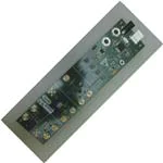
Figure 1. CDCE421A Evaluation Board
Features:
• Easy-to-use evaluation board to generate low phase noise clocks between 10.9 MHz and 1.175 GHz
• Easy device programming via host-powered USB port
• Fast configuration through GUI software interface
• Total board power provided either through USB port or separate 3.3-V and ground connections
• LVCMOS input interface or crystal input
• Standard 6-pin XO package connection available
space
Contents
Windows is a registered trademark of Microsoft Corporation.
All other trademarks are the property of their respective owners.
SCAU031 – June 2009
Submit Documentation Feedback
10.9-MHz to 1.175-GHz, Low Phase Noise Clock Evaluation Board
1
�www.ti.com
1
2
3
4
5
6
7
8
General Description ......................................................................................................... 3
Signal Path and Control Circuitry .......................................................................................... 3
Block Description ............................................................................................................ 4
Software-Selectable Options ............................................................................................... 4
Installing the GUI Software and USB Driver ............................................................................. 5
Chronos GUI Software ...................................................................................................... 7
Configuring the Board ..................................................................................................... 10
Schematics and Layout .................................................................................................... 11
List of Figures
1
2
3
4
5
6
7
8
9
10
11
12
13
2
CDCE421A Evaluation Board .............................................................................................. 1
Enabled (Block A) and Disabled (Blocks B, C, D) Switch Positions .................................................. 3
Software Installation Screen 1 ............................................................................................. 5
Software Installation Screen 2 ............................................................................................. 6
TI Chronos GUI Window .................................................................................................... 7
Loop Filter Configuration Pop-Up Dialog ................................................................................. 8
CDCE421A Advanced Controls Pop-Up Dialog ......................................................................... 9
JP1 Settings................................................................................................................. 11
CDCE421AEVM—Schematic ............................................................................................. 12
CDCE421AEVM—Schematic ............................................................................................. 13
CDCE421AEVM—Schematic ............................................................................................. 14
CDCE421AEVM—Schematic ............................................................................................. 15
CDCE421AEVM—Schematic ............................................................................................. 16
10.9-MHz to 1.175-GHz, Low Phase Noise Clock Evaluation Board
SCAU031 – June 2009
Submit Documentation Feedback
�General Description
www.ti.com
1
General Description
The CDCE421A is a high-performance, low phase noise clock generator. It has two fully integrated,
low-noise, LC-based voltage-controlled oscillators (VCOs) that operate in the range of 1.75 GHz to 2.35
GHz.
The CDCE421A has an integrated crystal oscillator circuitry that operates in conjunction with an external
AT-cut crystal to produce a stable frequency reference for the PLL-based frequency synthesizer. A 3.3-V
LVCMOS level input can also be used instead of a crystal to provide a frequency reference to the PLL.
This evaluation module (EVM) is designed to demonstrate the electrical performance of the CDCE421A.
This fully assembled and factory-tested evaluation board allows complete validation of the CDCE421A
device functionalities. Throughout this document, the acronym EVM and the phrases evaluation module
and evaluation board are synonymous with the CDCE421AEVM. Figure 1 illustrates the CDCE421AEVM.
For optimum performance, the board is equipped with 50-Ω SMA connectors and well-controlled, 50-Ω
impedance microstrip transmission lines.
2
Signal Path and Control Circuitry
The CDCE421A can accept a 29-MHz to 44-MHz frequency input from either an LVCMOS source (up to
3.3 V) or a crystal in the same frequency range.
The CDCE421AEVM is divided into four blocks. The programming section and device power for each
block can be enabled or disabled through individual switches provided for each block. For example, in
order to enable power and programming for Block A, the switch must be in the position shown in Figure 2.
The other blocks are disabled with the respective switches as the figure illustrates.
For more information about the CDCE421A, see the CDCE421A product data sheet available for
download from the TI web site (www.ti.com).
Figure 2. Enabled (Block A) and Disabled (Blocks B, C, D) Switch Positions
SCAU031 – June 2009
Submit Documentation Feedback
10.9-MHz to 1.175-GHz, Low Phase Noise Clock Evaluation Board
3
�Block Description
3
www.ti.com
Block Description
This section summarizes the function of each block.
3.1
Block A
Block A includes a CDCE421A QFN device that accepts an LVCMOS reference input through the vertical
SMA input connector (Ref Input), which is already ac-coupled onboard the EVM.
3.2
Block B
This block includes a CDCE421A QFN device that uses an AT crystal. This block can be used as either a
crystal oscillator (XO) or a voltage-controlled crystal oscillator (VCXO). For use as an XO or VCXO, the
crystal should be mounted on either of the two crystal footprints on the board, and a vertical SMA input
connector must be installed on the provided footprint to be used as the control voltage input.
3.3
Block C
Block C can accommodate a 5 × 7 crystal oscillator. The oscillator package must also include a
fixed-frequency crystal with a specified load and range.
3.4
Block D
Block D includes a socket that fits the oscillator part used in block C.
The output frequency of the CDCE421A is always an integer multiple or integer divide of the input
frequency. The output frequency is determined through the selection of VCO1 or VCO2 and the
appropriate prescalar and output divider based on the values discussed in the CDCE421A product data
sheet.
The loop filter selection will affect the output frequency phase noise, and should be considered in
conjunction with the type of input used.
In LVDS mode, the device can achieve up to 400 MHz. In LVPECL mode, the device can achieve up to
1.175 GHz. The output signaling level and LVPECL termination are selectable through the software
interface.
4
Software-Selectable Options
The provided graphical user interface (GUI) software allows users to easily send commands to the
CDCE421A through the host-powered USB interface. The EVM includes a slave USB controller that
transmits the commands to the single-pin programming interface located on the CDCE421A. DC power for
the USB controller can either be derived from the 5-V power pin in the USB cable or by using an external
5-V ac adapter in the slot available on the EVM.
In addition to writing commands to the CDCE421A SRAM while the board is powered up, commands can
also be stored in either the nonvolatile USB microcontroller memory or the EEPROM included within the
CDCE421A. This option allows users to start the EVM in the desired state without requiring additional
programming at power-up.
Note:
4
The CDCE421A does have a permanent EEPROM lock mode. After this mode, is selected
the EEPROM within the CDCE421A cannot be changed. This option is useful when setting
final configurations.
10.9-MHz to 1.175-GHz, Low Phase Noise Clock Evaluation Board
SCAU031 – June 2009
Submit Documentation Feedback
�Installing the GUI Software and USB Driver
www.ti.com
5
Installing the GUI Software and USB Driver
To start the software installation, run the CDCE421A Control GUI v 1.0.msi, software, available in the
CDCE421A product folder on TI.com. The screen shown in Figure 3 appears.
Figure 3. Software Installation Screen 1
SCAU031 – June 2009
Submit Documentation Feedback
10.9-MHz to 1.175-GHz, Low Phase Noise Clock Evaluation Board
5
�Installing the GUI Software and USB Driver
www.ti.com
Note the location of the installation folder because the USB driver must be installed to the same folder
after setup completes and the USB cable is connected, as indicated in Figure 4.
Figure 4. Software Installation Screen 2
After the setup wizard completes, start the GUI interface from the Windows® Start menu (Start→Texas
Instruments→Chronos Eval↑TIChronosGUI.exe).
Connect the USB cable to the EVM. If Windows prompts you for an appropriate driver, do not use the
automatic search option. Instead, select the manual search, and when prompted for the driver location,
browse to the Chronos GUI file folder that was used during instillation. (No action is needed if Windows
does not prompt you for a different driver.)
Once the USB driver installation completes, the GUI software should load properly and be ready for use. A
green light in the USB communication box indicates a good USB connection; a red light indicates a faulty
USB connection. If you get a red light in the communication box, make sure that the correct USB driver is
properly installed and the USB cable is properly connected to the EVM.
6
10.9-MHz to 1.175-GHz, Low Phase Noise Clock Evaluation Board
SCAU031 – June 2009
Submit Documentation Feedback
�Chronos GUI Software
www.ti.com
6
Chronos GUI Software
Figure 5 illustrates the TI Chronos GUI software display.
Figure 5. TI Chronos GUI Window
6.1
Using Software-Enabled Automatic PLL Selection
The screenshot displayed in Figure 5 shows the on-chip PLL structure of the CDCE421A. In this display,
the user can change the Input Frequency, PFD Charge Pump, Loop Filter, and Output settings. The
balance of the settings are selected by the software with user-selectable options as described in the steps
below.
Step 1. IC Config and Input Calculator
Before programming the PLL, the EVM block that is being programmed must be selected in the IC
Block Config section of the GUI. For any block in the EVM that is being used, the first row of
calculations is useful when trying to investigate the input frequency to the CDCE421A required in order
to obtain a desired output frequency. The input is found by pressing the Calculate button.
Step 2. Store Crystal Frequency
If a crystal input is used in Block B of the EVM, the crystal frequency must be entered into the space
provided by clicking on the Device_EEPROM field found at the top of the software GUI. This action
opens a drop-down menu, where the user can click the menu item labeled Save Block B – XTAL Freq
to EEPROM. In this field, enter the crystal frequency in the format xx.xxx,specified in MHz.
Step 3. Output Calculator and Apply PLL Settings
The second row of calculations is used to get the PLL settings required to obtain a particular output
frequency provided by a given input frequency to CDCE421A. The input must be entered in the second
row as well as the place provided at the input of the PLL block diagram. After the Calculate button is
pressed, the adjacent drop-down menu is populated with several choices for the given input; the
desired output can then be chosen from this list. Choosing an output then sets the divider settings
within the PLL. Click on the Apply button (next to the drop-down menu) to write the PLL settings to the
SCAU031 – June 2009
Submit Documentation Feedback
10.9-MHz to 1.175-GHz, Low Phase Noise Clock Evaluation Board
7
�Chronos GUI Software
www.ti.com
device SRAM. If LVPECL output is desired, scroll through the Output type box until LVPECL is
displayed. This option automatically enables onboard LVPECL termination. If LVDS output is desired,
scroll through the Output type box until LVDS is displayed.
Step 4. PLL Bandwidth Select
If the user wants to adjust the PLL bandwidth, the Loop Filter block must be clicked. Clicking this block
brings up a pop-up screen, as shown in Figure 6.
Figure 6. Loop Filter Configuration Pop-Up Dialog
For a clean reference input to CDCE421A (such as from an oscillator or crystal), the maximum
bandwidth and phase margin settings must be used, or 400 kHz and 80 degrees, respectively. The
PDF charge pump current must be set to its maximum (224 µA). The PFD charge pump current can be
set by clicking on the PDF Charge Pump block. This selection then presents a drop-down menu with
the various charge pump current settings.
For a dirty reference input to CDCE421A, use the minimum bandwidth setting (50 kHz). Additionally, to
reduce the output jitter for a dirty input, the phase margin can be reduced to near-minimum (30
degrees), depending on the integration limits of the jitter that is deemed important for a given
application. To reduce the output jitter even further, reduce the charge pump current to near-minimum
(56 µA), depending on the integration limits of the jitter.
Step 5. Write to CDCE421A EEPROM
To write any particular setting to the EEPROM (in locking or no-locking mode), the menu item at the
top of the GUI titled Device_EEPROM must be clicked. This action highlights the items Write settings
to EEPROM (No locking) and Write settings to EEPROM (Locking) as part of a drop-down menu.
Choose the appropriate option after setting the desired PLL configurations in order to write to the
EEPROM in the appropriate mode.
8
10.9-MHz to 1.175-GHz, Low Phase Noise Clock Evaluation Board
SCAU031 – June 2009
Submit Documentation Feedback
�Chronos GUI Software
www.ti.com
6.2
Manual PLL Block Selection (Advanced Control)
This GUI helps users to set the PLL without having to manually alter all the blocks individually within the
PLL. If a user is familiar with the general operation of PLLs, one may activate individual control of the PLL
blocks by clicking on the Advanced Control button. A new window appears, as shown in Figure 7.
Figure 7. CDCE421A Advanced Controls Pop-Up Dialog
Table 1 summarizes the various menu options available in this dialog window.
Table 1. Advanced Control: Software Setting Options
Section
VCO Select
Prescalar
Output Divider.
Function
Selects between VCO1 and VCO2. Only one VCO can be
used during operation. See the CDCE421A product data
sheet for VCO tuning ranges.
The prescalar selection will be determined in conjunction with
the VCO and output divider selection. See the CDCE421A
product data sheet to determine the proper setting.
The output divider will be determined in conjunction with the
VCO and prescalar settings. See the CDCE421A product
data sheet to determine the proper setting.
Driver Select
Selects between LVPECL or LVDS.
PECL config
This option should be activated with using LVPECL output.
When selected, the USB controller will enable onboard
LVPECL termination.
Charge Pump Current.
Selects appropriate charge pump current. See screen
shotsxx for recommended configurations.
Loop Filter Bias Select
Bias 0 should be used at all times. Bias 1 is a reserved test
mode for TI.
SCAU031 – June 2009
Submit Documentation Feedback
10.9-MHz to 1.175-GHz, Low Phase Noise Clock Evaluation Board
9
�Configuring the Board
www.ti.com
Table 1. Advanced Control: Software Setting Options (continued)
Section
Function
Loop Filter
Selects the loop filter C and R values. See screen shotsxx for
recommended configurations.
VCO Calibration
TI Test Use
This setting should be kept at 0000 ibias_100ua. Other
settings are for TI internal use only.
Chronos IC Config
• Select Use U13 programming socket for rapid
programming of Chronos-enabled devices.
• Select Use U8 DIE/U9 QFN socket if the EVM is using a
direct-mounted die OR a QFN-mounted device. Note:
This setting is the typical configuration.
• Select Use U12XTAL EVAL if using the optional 6 pin
XO mounting pads (for Chronos-enabled oscillators).
Chronos Control
• Select Enable Power to run the entire board from the
host USB voltage. In this mode, the EVM will not need
an external 3.3-V power supply. If this option is not
selected, then a 3.3-V supply and ground connection
must be attached.
• Select Output Enable to provide a clock output. When
not selected, the output will go to a high-Z state.
• Push Write Chronos settings to RAM to download
settings to the CDCE421A onboard volatile SRAM.
These settings will be lost upon power down.
• Push Write Chronos settings to EEPROM NO LOCKING
when ready to store the configuration in the CDCE421A
nonvolatile EEPROM. The settings will be available after
power down. The settings can be changed at a later
time.
• Push Write Chronos settings to EEPROM LOCKING
only if the settings are permanent and final. After this
selection, the EEPROM will be locked and cannot be
altered at a later time.
USB communication
7
When Enable VCO Calibration is selected, the CDCE421A
will use its internal calibration circuit to lock the PLL loop.
VCO Calibration Override should not be checked. (TI uses
manual calibration for test modes.)
A bright red light indicates that USB is not connected or not
communicating properly. A green light indicates a proper
USB connection.
Configuring the Board
The CDCE421AEVM can be powered from either the USB power supply or from an external source. The
CDCE421AEVM only requires a USB cable to be attached for programming purposes; however, for test
measurements, it is recommended to also use an external 3.3-V power supply. Test measurements can
also be taken with only the USB-supplied power. However, as a result of USB power variances, results
may degrade. It is also possible to program the CDCE421A and then disconnect the USB cable with minor
board configuration changes. To enable power and programming of any of the four blocks on the
CDCE421AEVM, the respective switch must be turned on, as explained earlier (see Section 2).
7.1
Configuration for Programming and Testing (with USB Cable Attached)—Default
Configuration
The CDCE421AEVM is configured by default to operate with the USB cable attached and a 3.3-V power
supply added to AUX VDD and GND. In this configuration, the USB microcontroller is powered by the USB
port 5-V supply while the CDCE421A is powered by the 3.3-V external supply. This setup is optimal for
programming the CDCE421A while also taking measurements. This configuration removes the power
variation found in USB power supplies by isolating the CDCE421A from the USB supply.
10
10.9-MHz to 1.175-GHz, Low Phase Noise Clock Evaluation Board
SCAU031 – June 2009
Submit Documentation Feedback
�Schematics and Layout
www.ti.com
7.2
Configuration for Programming (with USB Cable Attached)
The CDCE421AEVM can also use power supplied through the USB cable as its sole power source.
However, as mentioned earlier, because of power-supply variances in the USB supply, this configuration
is not recommended for measurements. This setup is helpful for saving configuration settings to the
CDCE421A and then later powering the device from its internal memory (a useful option if there is no USB
port available on a PC in a lab or test chamber). In this configuration, JP1 must be moved from its default
position to the new position shown in Figure 8. Additionally, the Enable (onboard) Power box must be
checked on the GUI software, followed by pushing the Apply software button.
Figure 8. JP1 Settings
7.3
Configuration for Testing from a Saved Configuration (with USB Cable Removed after
Programming)
When operating the CDCE421A without the USB programming cable, the CDCE421AEVM must be
pre-programmed in one of the configurations discussed in this section and then reconfigured for external
power-supply usage.
Before making these board modifications, the CDCE421A settings must be saved with one of the above
USB cable attached configurations. Use the Write Chronos Settings to EEPROM NO LOCKING software
button to save the CDCE421A settings to the device-internal EEPROM. After the settings are saved to the
EEPROM, the USB cable can be removed. Once the cable has been disconnected, jumper JP1 should be
in the Using External 3.3-V Supply position (as shown in Figure 8). The EVM is now ready for use without
the USB cable connected. The CDCE421A will always start from its saved configuration state in this
mode.
If the CDCE421A must be isolated from the microcontroller, the switch that corresponds to the block in
use should be set to Off for CE_x, SDATA_x, and LVPECL_TERM_x (where x represents the block
name). The power line switch for that block, however, should be kept on. This sequence also allows for
the USB cable to be removed without affecting performance while the CDCE421A is powered up.
8
Schematics and Layout
Figure 9 through Figure 11 show the printed circuit board (PCB) schematics for the CDCE421AEVM.
Note:
Board layouts are not to scale. These figures are intended to show how the board is laid out;
they are not intended to be used for manufacturing CDCE421AEVM PCBs.
SCAU031 – June 2009
Submit Documentation Feedback
10.9-MHz to 1.175-GHz, Low Phase Noise Clock Evaluation Board
11
�J3
D8 D9
+5V
5
RESET1
1
2
3
4
1
2
R30 1.5k
2
24LC512
A0
Vcc
A1
WP
A3 SCL
Vss SDA
2
0.1uF
U4
C28
1uF
C43
R21
15K
8
7
6
5
+5V
C40
+3V3
U1
1
R4
2
2
33pF
33pF
EEPROM_WP
SCL
SDA
2 R50
1M
C29
RESET#
SENSE
OUT2
OUT1
21
12
11
14
13
15
16
20
19
18
17
+3V3
R49
1.5k
+3V3
MMBT4401
NPN
2N2222A
Q1
PUR
3
TPS77333DGK
GND
EN#
IN2
IN1
U2
R51
1.5k
+3V3
2
C32
1
1
SCL
SDA
1.5k
1
15k R5
4
1uF
6
5
TPS76701QPWP
3
2
OUT2
OUT1
FB
_RESET
GND/HS8
GND/HS7
NC1
NC2
NC3 GND/PWRPAD
GND/HS3 GND/HS6
GND/HS4 GND/HS5
IN1
IN2
EN_
C38
8
9
10
6
7
5
12MHZ1
ECS-120-S-5P-TR
0.1uF 0.1uF
C41
+3V3
R6 2
R7 2
+3V3
0.1uF
C42
+3V3
1 33
4
DP 3
GND
1 33
MBRS2040LT3
1uF
C33
PWR_EN
DM 2
+5V 1
+3V3
1
J1
R31 1.5k
1
5
6
Type B USB-Shield
3 1
2
2
1
8
7
5
24
42
59
10
39
62
61
60
14
15
20
13
12
11
21
38
37
16
17
18
19
POR
450
+
TUSB3210
GND1
GND2
GND3
GND4
VCC1
VCC2
VCC3
X1
X2
TEST0
TEST1
TEST2
RST
SCL
SDA
SELF/BUS
VREN
VDDOUT
SUSP
PUR
DP0
DM0
1
R79
+
+3V3
2
250
2
JP1
C35
22uF/20V Low ESR
C31
22uF/20V Low ESR
1
R85
P4
3
2
P2.0
P2.1
P2.2
P2.3
P2.4
P2.5
P2.6
P2.7
P1.0
P1.1
P1.2
P1.3
P1.4
P1.5
P1.6
P1.7
P00
P01
P02
P03
P04
P05
P06
P07
S2
S3
P30/RxD/S0
P31/TxD/S1
P32
P33/INT1
P34/T0
P35
P36
P37
1
VDD_EX
R97
301
S2 2
10k R93
1
+3V3
Costumer EVM Revission Control S2=1 S3=0
Lab EVM Revission Control S2=0 S3=0
8
9
VDD_A_ON
VDD_B_ON
VDD_C_ON
VDD_D_ON
OPAMP_RD_A
OPAMP_RD_B
OPAMP_RD_C
OPAMP_RD_D
22
23
25
26
27
28
29
30
58
57
56
55
54
53
52
51
SDATA_A
CE_A
SDATA_B
CE_B
SDATA_C
CE_C
SDATA_D
CE_D
R59
10k
+3V3
D25 Communication
LED GREEN
R65
301
+3V3
Power
Power
D26 Device
LED GREEN
R66
301
VDD
D24 Control
LED GREEN
31
32
33
34
35
36
40
41
43
44
45
46
47
48
49
50
VDD
10uF/6.3V
C37
+3V3
1
2
U3
1
2
1
GND/HS1
GND/HS2
GND
NC
2
1
2
1
Adaptor 5VDC
2
3
1
4
POR
SW_PUSHBUTTON_5PIN
1
2
2
1
2
1
+5V
1
2
Good
2
R80
1
Default
Default
Default
Default
R82
10k
=
=
=
=
LVPECLTermination
LVPECLTermination
LVPECLTermination
LVPECLTermination
OPAMP_EN_A
OPAMP_EN_B
OPAMP_EN_C
OPAMP_EN_D
R81
10k
+3V3
VDD_ON
Q4
2N2222A
Enable only one OP-AMP at a time
R72
10k
+3V3
R78
2
2
10k
+3V3
R71
10k
+3V3
LVPECL_TERM_A
LVPECL_TERM_B
LVPECL_TERM_C
LVPECL_TERM_D
VDD_ON
PWR_EN
1
1
100k
R77
1
100k -NP
VDD
+3V3
2
1
1
2
3
4
1
2
2
1
3
2
GND
1
2
3
4
6
7
63
64
1
2
3
4
6
7
63
64
2
1
10.9-MHz to 1.175-GHz, Low Phase Noise Clock Evaluation Board
2
12
1
P5
Schematics and Layout
www.ti.com
Figure 9. CDCE421AEVM—Schematic
SCAU031 – June 2009
Submit Documentation Feedback
(EXT Supply 5V)
�CE_A
6
3
VDD
R61
10K- NP
TDA04H0SK1
5
7
2
4
8
C70
0.1uF
R70
49.9
REF. A INPUT
1
J100
SMA-VERT
LVPECL_TERM_A
SDATA_A
2
3
4
5
1
1
2
VDD
1
2
SW1
1
2
R68
10K- NP
R113
422
2
1
VDD
R112
422
2
1
1
301
2
2
4
5
6
19
15
24
14
23
22
21
1
3
1
NC1
NC2
NC3
NC4
C112
GND1
GND2
OUTP
OUTN
VCC1
VCC2
25
11
12
13
VDD_A_ON
R58
150
FDV303N
Q10
Q5
2N2222A
R99
10k
CDCE421_24QFN VDD
PWRPAD
NC5
NC6
NC7
18
20
8
9
10
7
16
17
0.1uF 0.1uF
C111
R107
2
1
TESTEN TESTOUTA
SCANEN
SCANIN SCANOUT
VCTL
XIN2_VCXO
XIN2_XO
XIN1
1uF
C64
100k
R109 10k
1
2
CE
SDATA
U11
D27
LED GREEN
R103
+3V3
3
2
VDD
2
2
1
1
2
R94
10k
2
1
1
2
FDV303N
Q18
R55
150
R95
10k
4
3
2
1
5
6
7
8
SMA-VERT
J24
C60 1
0.1uF
C59 1
0.1uF
J14
SMA-VERT
+3V3
NC2
OUT
V+
SHDN
TLV3501
C65 0.1uF
V-
+IN
-IN
NC1
U17
5
4
3
2
5
4
3
2
SCAU031 – June 2009
Submit Documentation Feedback
1
OPAMP_RD_A
+3V3
OPAMP_EN_A
www.ti.com
Schematics and Layout
Figure 10. CDCE421AEVM—Schematic
10.9-MHz to 1.175-GHz, Low Phase Noise Clock Evaluation Board
13
�5
4
6
5
1
0.1uF
C106
3
4
Crystal
6
3
2
XXMhz1
7
2
TDA04H0SK1
8
SW2
1
1
J212
SMA-VERT
LVPECL_TERM_B
SDATA_B
CE_B
VDD
2
3
4
5
R118
422
2
1
R119
422
2
1
301
2
R100
10k
2
4
5
6
19
15
24
14
23
22
21
1
3
D28
LED GREEN
R104
VDD
1
C63
1uF
GND1
GND2
OUTP
OUTN
VCC1
VCC2
NC1
NC2
NC3
NC4
CDCE421_24QFN
PWRPAD
NC5
NC6
NC7
25
11
12
13
18
20
8
9
10
7
16
17
0.1uF 0.1uF
C109 C110
R108
2
1
TESTEN TESTOUTA
SCANEN
SCANIN SCANOUT
VCTL
XIN2_VCXO
XIN2_XO
XIN1
CE
SDATA
U9
1
100k
R110 10k
1
2
3
2
+3V3
R56
150
FDV303N
Q9
Q6
2N2222A
VDD_B_ON
2
1
R91
10k
1
2
VDD
2
1
2
1
1
10.9-MHz to 1.175-GHz, Low Phase Noise Clock Evaluation Board
2
FDV303N
Q16
R54
150
R92
10k
4
3
2
1
C62
V-
+IN
-IN
5
6
7
8
OPAMP_EN_B
OPAMP_RD_B
+3V3
J11
SMA-VERT
OUTPUT
SMA-VERT
J21
C49 1
0.1uF
C48 1
0.1uF
+3V3
NC2
OUT
V+
SHDN
TLV3501
0.1uF
NC1
U16
5
4
3
2
14
5
4
3
2
VDD
Schematics and Layout
www.ti.com
Figure 11. CDCE421AEVM—Schematic
SCAU031 – June 2009
Submit Documentation Feedback
�VDD
J217
LVPECL_TERM_C
SDATA_C
CE_C
SMA-VERT
2
3
4
5
1
2
0.1uF
C108 R86 100k -NP
1
5
4
TDA04H0SK1
6
7
2
3
8
1
SW3
2
2
R121 R120
422
422
2
1
R84 0
1
R96 0 -NP
1
1
301
2
3
2
7
1
1
1uF
C47
C117
OUTP
OUTN
VCC
VDD_C_ON
R63
150
FDV303N
Q11
Q7
2N2222A
R101
10k
VDD
4
5
6
0.1uF 0.1uF
C116
R111
2
1
CDCE421_OSC
GND
SDATA
SPARE
CE
U12
D29
LED GREEN
R105
100k
R114 10k
1
2
3
2
2
1
+3V3
2
1
R89
10k
1
2
VDD
2
1
2
1
1
2
FDV303N
Q17
R57
150
R90
10k
4
3
2
1
C61
V-
+IN
-IN
+3V3
NC2
OUT
V+
SHDN
TLV3501
0.1uF
NC1
U15
OPAMP_RD_C
+3V3
OPAMP_EN_C
J12
SMA-VERT
OUTPUT
SMA-VERT
J22
C52 1
0.1uF
C51 1
0.1uF
5
6
7
8
5
4
3
2
SCAU031 – June 2009
Submit Documentation Feedback
5
4
3
2
VDD
www.ti.com
Schematics and Layout
Figure 12. CDCE421AEVM—Schematic
10.9-MHz to 1.175-GHz, Low Phase Noise Clock Evaluation Board
15
�LVPECL_TERM_D
SDATA_D
CE_D
VDD
5
4
TDA04H0SK1
6
7
2
3
8
1
SW4
R123
422
2
1
2
2
R122
422
R87 0
R98 0
1
1
3
2
7
1
1
301
2
C46
OUTP
OUTN
VCC
1uF
CDCE421_SOCKET
GND
SDATA
SPARE
CE
U13
D30
LED GREEN
R106
1
100k
4
5
6
VDD_D_ON
R64
150
FDV303N
Q13
Q8
2N2222A
R102
10k
VDD
0.1uF 0.1uF
C105 C107
R115
2
1
R116 10k
1
2
3
2
2
1
+3V3
2
1
R83
10k
1
2
VDD
2
1
2
1
1
10.9-MHz to 1.175-GHz, Low Phase Noise Clock Evaluation Board
2
FDV303N
Q15
R62
150
R88
10k
4
3
2
1
C55
V-
+IN
-IN
+3V3
NC2
OUT
V+
SHDN
TLV3501
0.1uF
NC1
U14
5
6
7
8
SMA-VERT
J23
C54 1
0.1uF
C53 1
0.1uF
J13
SMA-VERT
OPAMP_RD_D
+3V3
OPAMP_EN_D
5
4
3
2
16
5
4
3
2
VDD
Schematics and Layout
www.ti.com
Figure 13. CDCE421AEVM—Schematic
SCAU031 – June 2009
Submit Documentation Feedback
�EVALUATION BOARD/KIT IMPORTANT NOTICE
Texas Instruments (TI) provides the enclosed product(s) under the following conditions:
This evaluation board/kit is intended for use for ENGINEERING DEVELOPMENT, DEMONSTRATION, OR EVALUATION PURPOSES
ONLY and is not considered by TI to be a finished end-product fit for general consumer use. Persons handling the product(s) must have
electronics training and observe good engineering practice standards. As such, the goods being provided are not intended to be complete
in terms of required design-, marketing-, and/or manufacturing-related protective considerations, including product safety and environmental
measures typically found in end products that incorporate such semiconductor components or circuit boards. This evaluation board/kit does
not fall within the scope of the European Union directives regarding electromagnetic compatibility, restricted substances (RoHS), recycling
(WEEE), FCC, CE or UL, and therefore may not meet the technical requirements of these directives or other related directives.
Should this evaluation board/kit not meet the specifications indicated in the User’s Guide, the board/kit may be returned within 30 days from
the date of delivery for a full refund. THE FOREGOING WARRANTY IS THE EXCLUSIVE WARRANTY MADE BY SELLER TO BUYER
AND IS IN LIEU OF ALL OTHER WARRANTIES, EXPRESSED, IMPLIED, OR STATUTORY, INCLUDING ANY WARRANTY OF
MERCHANTABILITY OR FITNESS FOR ANY PARTICULAR PURPOSE.
The user assumes all responsibility and liability for proper and safe handling of the goods. Further, the user indemnifies TI from all claims
arising from the handling or use of the goods. Due to the open construction of the product, it is the user’s responsibility to take any and all
appropriate precautions with regard to electrostatic discharge.
EXCEPT TO THE EXTENT OF THE INDEMNITY SET FORTH ABOVE, NEITHER PARTY SHALL BE LIABLE TO THE OTHER FOR ANY
INDIRECT, SPECIAL, INCIDENTAL, OR CONSEQUENTIAL DAMAGES.
TI currently deals with a variety of customers for products, and therefore our arrangement with the user is not exclusive.
TI assumes no liability for applications assistance, customer product design, software performance, or infringement of patents or
services described herein.
Please read the User’s Guide and, specifically, the Warnings and Restrictions notice in the User’s Guide prior to handling the product. This
notice contains important safety information about temperatures and voltages. For additional information on TI’s environmental and/or
safety programs, please contact the TI application engineer or visit www.ti.com/esh.
No license is granted under any patent right or other intellectual property right of TI covering or relating to any machine, process, or
combination in which such TI products or services might be or are used.
FCC Warning
This evaluation board/kit is intended for use for ENGINEERING DEVELOPMENT, DEMONSTRATION, OR EVALUATION PURPOSES
ONLY and is not considered by TI to be a finished end-product fit for general consumer use. It generates, uses, and can radiate radio
frequency energy and has not been tested for compliance with the limits of computing devices pursuant to part 15 of FCC rules, which are
designed to provide reasonable protection against radio frequency interference. Operation of this equipment in other environments may
cause interference with radio communications, in which case the user at his own expense will be required to take whatever measures may
be required to correct this interference.
EVM WARNINGS AND RESTRICTIONS
It is important to operate this EVM within the input voltage range of –0.5 V to +4.0 V and the output voltage range of 0 to +3.6 V.
Exceeding the specified input range may cause unexpected operation and/or irreversible damage to the EVM. If there are questions
concerning the input range, please contact a TI field representative prior to connecting the input power.
Applying loads outside of the specified output range may result in unintended operation and/or possible permanent damage to the EVM.
Please consult the EVM User's Guide prior to connecting any load to the EVM output. If there is uncertainty as to the load specification,
please contact a TI field representative.
During normal operation, some circuit components may have case temperatures greater than +120°C. The EVM is designed to operate
properly with certain components above +85°C as long as the input and output ranges are maintained. These components include but are
not limited to linear regulators, switching transistors, pass transistors, and current sense resistors. These types of devices can be identified
using the EVM schematic located in the EVM User's Guide. When placing measurement probes near these devices during operation,
please be aware that these devices may be very warm to the touch.
Mailing Address: Texas Instruments, Post Office Box 655303, Dallas, Texas 75265
Copyright © 2009, Texas Instruments Incorporated
�IMPORTANT NOTICE
Texas Instruments Incorporated and its subsidiaries (TI) reserve the right to make corrections, modifications, enhancements, improvements,
and other changes to its products and services at any time and to discontinue any product or service without notice. Customers should
obtain the latest relevant information before placing orders and should verify that such information is current and complete. All products are
sold subject to TI’s terms and conditions of sale supplied at the time of order acknowledgment.
TI warrants performance of its hardware products to the specifications applicable at the time of sale in accordance with TI’s standard
warranty. Testing and other quality control techniques are used to the extent TI deems necessary to support this warranty. Except where
mandated by government requirements, testing of all parameters of each product is not necessarily performed.
TI assumes no liability for applications assistance or customer product design. Customers are responsible for their products and
applications using TI components. To minimize the risks associated with customer products and applications, customers should provide
adequate design and operating safeguards.
TI does not warrant or represent that any license, either express or implied, is granted under any TI patent right, copyright, mask work right,
or other TI intellectual property right relating to any combination, machine, or process in which TI products or services are used. Information
published by TI regarding third-party products or services does not constitute a license from TI to use such products or services or a
warranty or endorsement thereof. Use of such information may require a license from a third party under the patents or other intellectual
property of the third party, or a license from TI under the patents or other intellectual property of TI.
Reproduction of TI information in TI data books or data sheets is permissible only if reproduction is without alteration and is accompanied
by all associated warranties, conditions, limitations, and notices. Reproduction of this information with alteration is an unfair and deceptive
business practice. TI is not responsible or liable for such altered documentation. Information of third parties may be subject to additional
restrictions.
Resale of TI products or services with statements different from or beyond the parameters stated by TI for that product or service voids all
express and any implied warranties for the associated TI product or service and is an unfair and deceptive business practice. TI is not
responsible or liable for any such statements.
TI products are not authorized for use in safety-critical applications (such as life support) where a failure of the TI product would reasonably
be expected to cause severe personal injury or death, unless officers of the parties have executed an agreement specifically governing
such use. Buyers represent that they have all necessary expertise in the safety and regulatory ramifications of their applications, and
acknowledge and agree that they are solely responsible for all legal, regulatory and safety-related requirements concerning their products
and any use of TI products in such safety-critical applications, notwithstanding any applications-related information or support that may be
provided by TI. Further, Buyers must fully indemnify TI and its representatives against any damages arising out of the use of TI products in
such safety-critical applications.
TI products are neither designed nor intended for use in military/aerospace applications or environments unless the TI products are
specifically designated by TI as military-grade or "enhanced plastic." Only products designated by TI as military-grade meet military
specifications. Buyers acknowledge and agree that any such use of TI products which TI has not designated as military-grade is solely at
the Buyer's risk, and that they are solely responsible for compliance with all legal and regulatory requirements in connection with such use.
TI products are neither designed nor intended for use in automotive applications or environments unless the specific TI products are
designated by TI as compliant with ISO/TS 16949 requirements. Buyers acknowledge and agree that, if they use any non-designated
products in automotive applications, TI will not be responsible for any failure to meet such requirements.
Following are URLs where you can obtain information on other Texas Instruments products and application solutions:
Products
Amplifiers
Data Converters
DLP® Products
DSP
Clocks and Timers
Interface
Logic
Power Mgmt
Microcontrollers
RFID
RF/IF and ZigBee® Solutions
amplifier.ti.com
dataconverter.ti.com
www.dlp.com
dsp.ti.com
www.ti.com/clocks
interface.ti.com
logic.ti.com
power.ti.com
microcontroller.ti.com
www.ti-rfid.com
www.ti.com/lprf
Applications
Audio
Automotive
Broadband
Digital Control
Medical
Military
Optical Networking
Security
Telephony
Video & Imaging
Wireless
www.ti.com/audio
www.ti.com/automotive
www.ti.com/broadband
www.ti.com/digitalcontrol
www.ti.com/medical
www.ti.com/military
www.ti.com/opticalnetwork
www.ti.com/security
www.ti.com/telephony
www.ti.com/video
www.ti.com/wireless
Mailing Address: Texas Instruments, Post Office Box 655303, Dallas, Texas 75265
Copyright © 2009, Texas Instruments Incorporated
�