User's Guide
SCAU034 – June 2009
Two/Four Output Low Phase Noise Clock Evaluation
Board
1
2
3
4
5
6
7
8
Contents
Features .......................................................................................................................
General Description .........................................................................................................
Signal Path and Control Circuit ............................................................................................
Software Selectable Options ...............................................................................................
Installing the GUI Interface and USB Driver .............................................................................
TI CDCE62002 Control GUI Interface ....................................................................................
6.1
Using the EVM GUI.................................................................................................
Configuring the Board .......................................................................................................
CDCE62002EVM Board Schematic Diagram ............................................................................
2
2
3
3
4
4
5
7
9
List of Figures
1
2
3
4
5
6
7
8
9
CDCE62002EVM Evaluation Board .......................................................................................
Input Buffer Properties ......................................................................................................
Smart MUX ...................................................................................................................
Smart MUX ...................................................................................................................
Loop Filter, Internal Only....................................................................................................
Output Buffer Configuration (each output)................................................................................
Tools – Write to EEPROM ..................................................................................................
External Loop Filter selection switches ...................................................................................
Control Bus ON/OFF Dip Switches ........................................................................................
SCAU034 – June 2009
Submit Documentation Feedback
Two/Four Output Low Phase Noise Clock Evaluation Board
2
5
5
5
6
6
7
8
8
1
�Features
1
www.ti.com
Features
•
•
•
•
•
•
Easy to use Evaluation boards to generate low phase noise clocks between 4.25MHz and 1.175GHz
Easy device programming via host-powered USB port
Fast configuration through provided GUI software interface
Total board power provided either through USB port or separate 3.3V and ground connections
Single ended or differential input interface or crystal input
Crystal filter on output readily available for clocking high speed A/D converters
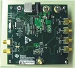
Figure 1. CDCE62002EVM Evaluation Board
2
General Description
The CDCE62002 is a high performance low phase noise frequency synthesizer and jitter cleaner. It has
two fully integrated low noise LC based Voltage Control Oscillators (VCOs) which operate in the
1.735GHz – 2.35GHz range. It provides support for two redundant inputs and using its on-chip PLL
architecture can provide up to two differential or four single ended low jitter outputs.
The CDCE62002 supports single ended and differential input signals as well as support for an integrated
crystal oscillator circuitry that operates in conjunction with an external AT-cut crystal to produce a stable
frequency reference for the PLL based frequency synthesizer.
The CDCE62002 can then be programmed through the SPI interface using the EVM programming GUI.
The evaluation module (EVM) is designed to demonstrate the electrical performance of the device. This
fully assembled and factory tested evaluation board allows complete validation of all device functions.
For optimum performance, the board is equipped with 50Ω SMA connectors and well-controlled 50Ω
impedance microstrip transmission lines.
2
Two/Four Output Low Phase Noise Clock Evaluation Board
SCAU034 – June 2009
Submit Documentation Feedback
�www.ti.com
3
Signal Path and Control Circuit
Signal Path and Control Circuit
The CDCE62002 provides support for selectable dual-inputs. One of the inputs is (PRI REF) can accept a
800kHz–500MHz frequency input from a differential signal source or a 800kHz–200MHz frequency input
from a single ended signal source. The second input (AUX IN) can support a crystal in the frequency
range of 2MHz to 42MHz or a single ended input (LVCMOS) up to 70MHz. The CDCE62002EVM provides
support for driving the AUX IN signal from an on-board 5mm x 3.2mm SMD crystal. If the AUX IN is
alternately driven by the SMA, the on-board crystal has to be removed and R65 should be populated with
a 0Ω resistor.
The CDCE62002 provides support for up to two differential (LVDS or LVPECL) or four single ended
(LVCMOS) or any combination of outputs in the range of 10.93MHz to 1.175GHz. The on-chip PLL
architecture can be configured such as to enable the device operated either as a jitter cleaner or a
frequency synthesizer or both.
The CDCE62002 provides support for either a completely internal loop filter or a partially external loop
filter. The loop filter selection will affect the output frequency phase noise and should be considered in
conjunction with the type of input used. If the CDCE62002 is to be used only as a frequency synthesizer,
the completely internal loop filter option is recommended. If the CDCE62002 is to be used as a jitter
cleaner, the partially external loop filter option is recommended.
For any output of the CDCE62002, its frequency is determined through selection of either of the device’s
on-chip twin VCOs, selection of one of the device’s two inputs, the input divider, the prescalar divider,
pre-configured internal loop filter settings or external loop filter and output divider, all of which are chosen
based on the CDCE62002 data sheet.
Each of the two outputs of the CDCE62002 can be selected through the software interface as a LVPECL
or LVDS or LVCMOS signaling level. The CDCE62002EVM provides support for on-board DC termination
for the LVPECL outputs through on-board jumper.
In LVCMOS mode the device can achieve up to 250MHz. In LVPECL mode the device can achieve up to
1.175GHz. In LVDS mode, the device can achieve up to 800MHz.
4
Software Selectable Options
The provided GUI software allows users to easily send commands to the CDCE62002 through the
host-powered USB interface. The EVM includes a slave USB controller that transmits the commands to
the SPI programming interface included on the CDCE62002. The DC power for the USB controller can
either be derived out of the 5V power pin in the USB cable or by using an external 5V AC adapter into the
slot available on the EVM. If the device is accessible for programming by the SPI programming interface
through the USB controller, the on-board LED D25 would be lit on power-up.
In addition to changing configuration to the CDCE62002 SRAM while the board is powered, configuration
can also be stored in EEPROM within the CDCE62002. This allows users to start the EVM in the desired
state without needing programming at power-up.
Note that the CDCE62002 does have a permanent EEPROM lock mode. After this mode is selected the
EEPROM within the CDCE62002 cannot be changed. This is useful when setting final configurations.
The CDCE62002EVM software also supports for the device GUI configurations to be saved into a .INI file,
which can be opened up at a later time with this GUI.
SCAU034 – June 2009
Submit Documentation Feedback
Two/Four Output Low Phase Noise Clock Evaluation Board
3
�Installing the GUI Interface and USB Driver
5
www.ti.com
Installing the GUI Interface and USB Driver
The CDCE62002 EVM Control GUI software requires that a Java Runtime Environment (JRE) to be
installed. The latest JRE is available as a free download at http://java.com. Install the JRE first, before
attempting to install the CDCE62002EVM GUI. To start the installation of the EVM software, double-click
on the file named “CDCE62002EVM installer.msi”.
Note the installation folder as the USB driver must be installed after the setup completes and the USB
cable is connected (first time only).
After the setup wizard completes start the GUI interface from the start menu (Start → Texas Instruments
Inc → CDCE62002 Software and Driver → CDCE62002).
Connect the USB cable to the EVM. If Windows asks for an appropriate driver, Do not use the automatic
search option! Select a manual installation and when prompted for the driver location browse to the
CDCE62002EVM program file folder that was used during instillation. If Windows does not ask for a driver,
no action is needed.
After USB driver installation the GUI software should connect properly and be ready for use. A green light
in the USB Status and SPI Bus Status boxes indicates good USB connection and a red light indicates
faulty USB connection or faulty SPI bus.
6
TI CDCE62002 Control GUI Interface
4
Two/Four Output Low Phase Noise Clock Evaluation Board
SCAU034 – June 2009
Submit Documentation Feedback
�TI CDCE62002 Control GUI Interface
www.ti.com
6.1
Using the EVM GUI
The graphical layout of the EVM GUI is based on the functional structure of the CDCE62002. By means of
the EVM GUI the user can change the Input Frequency, Input Divider, Input type, Input selection, PFD
Charge Pump, Internal/External Loop Filter, Output MUX selection, Output Divider, and Output type. Other
configuration settings are selected by the software with user-selectable options as described in the steps
below. If the power to the CDCE62002 is derived from the USB, the “Enable EVM Power” check box must
be checked. If the power to the CDCE62002 is derived from an external source, the “Enable EVM Power”
check box must be unchecked.
Step 1: Primary Reference
The primary reference input buffer section on the GUI can be clicked for a popup window that opens up,
as displayed below, showing selections on the external input signal type (differential or single ended), the
external signal connection to the CDCE62002 primary inputs (AC or DC termination), input buffer 5K
internal termination (enabled or disabled).
Figure 2. Input Buffer Properties
Step 2: Reference Input Selection through Smart MUX
The Smart MUX section of the GUI can be clicked for a popup window that opens up, as displayed below,
showing selections between PRI SEL (Primary Reference Select), AUX SEL (Auxiliary Input Select), or
AUTO Select between Primary Reference and Auxiliary Input with a preference to Primary Reference. A
Reference divider up to divide by 16 is available for the Primary Reference. In order for the Smart Mux to
work correctly in auto Mode the primary reference frequency should after the divider should be within 20%
of the frequency of the auxiliary input.
Figure 3. Smart MUX
Step 3: Input Divider Selection and PFD frequency
The Smart MUX section output feeds the input divider block where the signal can be divided up to 256.
The input divider output feeds the PFD. The output frequency of the input divider is what referred to is the
PFD frequency.
Figure 4. Smart MUX
SCAU034 – June 2009
Submit Documentation Feedback
Two/Four Output Low Phase Noise Clock Evaluation Board
5
�TI CDCE62002 Control GUI Interface
www.ti.com
Step3: Loop Filter Selection and Setup
The Loop Filter section of the GUI can be clicked for a popup window that opens up showing the internal
loop filter fixed configuration as displayed below. The values of the resistors and capacitors and the
charge pump output current of the internal active loop filter are fixed as displayed in the figure below. The
values are optimized for a 30.72MHz PFD frequency.
Figure 5. Loop Filter, Internal Only
Alternately, the loop filter can be configured to take external components with preselected charge pump
current and high pass filter component. To use External filter, an external loop filter setting from the drop
down menu with the desired charge pump current R3C3 values and only a single filter needs to be
enabled. Enabling the external preset filters can be achieved by selecting Switch 1,2,3 or 4 on Dip
Switches SW9 and SW10 at the back of the CDCE62002EVM. The external loop filter components (C1,
R2 and C2) for the loop filter are selected by the Dip Switches and the R3 and C3 are internal to the
device.
Step 7: Output Type Selection
The Output buffer section of the GUI for each of the outputs can be clicked for a popup window that opens
up, as displayed below, showing selections on each output clock source selectable between LVPECL (in
which cases the a jumper needs to be installed to enable a 150Ω termination resistor to ground), LVDS,
LVCMOS (in which case each of the P and N act as two separate LVCMOS outputs.
Figure 6. Output Buffer Configuration (each output)
6
Two/Four Output Low Phase Noise Clock Evaluation Board
SCAU034 – June 2009
Submit Documentation Feedback
�Configuring the Board
www.ti.com
Step 8: PLL Dividers Selection
The input, feedback and prescaler dividers can be selected by clicking on each tab in the GUI which
opens up a popup window displaying all the possible selections of those dividers. Care must be taken in
choosing these dividers, along with the VCO, charge pump and loop filter, such that the on-chip PLL of the
CDCE62002 can operate in a stable closed loop manner. Refer to the CDCE62002 data sheet for further
information on appropriate configuration of the PLL for closed loop operation. After the dividers are set
accordingly, the PLL LOCK indicator display on the GUI would be lit up in bright green color. Also the
on-board LED D33 would be lit to indicate PLL lock. The output dividers for each output can also be
chosen from possible selections displayed in the popup window which open up by clicking the output
divider tab in the GUI. Each output divider can also be disabled.
Step 9: Write to CDCE62002 EEPROM
To write any particular setting to the EEPROM (locked or unlocked), the menu item at the top of the GUI
titled “Tool” must be clicked which would highlight the items “Write EEPROM Unlocked” and “Write
EEPROM Locked” as part of a drop-down menu. Choosing the appropriate one after setting the desired
PLL configurations would result in writing to the EEPROM in its appropriate mode.
Figure 7. Tools – Write to EEPROM
7
Configuring the Board
The CDCE62002EVM can be powered from the USB power supply or from an external source. The
CDCE62002EVM only needs a USB cable attached for programming purposes however for test
measurements it is recommended to also use an external 3.3V power supply. Test measurements can
also be taken with only the USB supplied power however due to USB power variances results may
degrade. It is also possible to program the CDCE62002 and then disconnect the USB cable with minor
board configuration changes.
Configuration for Programming and Testing (with USB cable attached) (Default Configuration)
The CDCE62002EVM is configured by default to operate with the USB cable attached and a 3.3V power
supply added to EXT VDD and GND. In this configuration the USB microcontroller is powered by the USB
port’s 5V supply while the CDCE62002 is powered by the 3.3V external supply. This setup is optimal for
programming the CDCE62002 while also taking measurements. This configuration removes the power
variation found in USB power supplies by isolating the CDCE62002 from the USB supply.
Configuration for Programming (using USB power)
The CDCE62002EVM can use power supplied through the USB cable as its sole power source. However
due to power supply variances in the USB supply this configuration is not recommended for
measurements. This setup is for saving configuration settings to the CDCE62002 and later powering the
device from its internal memory (useful during performance testing of the device). In this configuration
JP_3_3 must be moved from its default position to the new position shown below. Also the “Enable EVM
Power” box must be checked on the EVM GUI interface software.
SCAU034 – June 2009
Submit Documentation Feedback
Two/Four Output Low Phase Noise Clock Evaluation Board
7
�Configuring the Board
www.ti.com
Configuration for On-board Reference Input Biasing
If the CDCE62002 EVM is designed to be used in AC termination with the internal 5K input termination to
VBB. The VBB voltage is controlled by the internal register settings. For more information about that VBB
voltage refer tot the data sheet.
In case other types of terminations to an external reference needs to be tested on the EVM, some
modifications needs to be made on the board to accomplish the measurement. C76, C77, R62, R63 and
R130 and the 2 Pin jumper that is feeding C112 can accommodate all possible combinations like
LVPECL-AC, LVPECL-DC, LVDS-AC and LVDC-DC terminations.
Configuration for On-board External Loop Filter
If the CDCE62002 is chosen to be operated as a jitter cleaner, it requires use of the partially external loop
filter which is located at the back side of the CDCE62002EVM. There are four external loop filter options
provided on the EVM. The external loop filter topology is as shown below.
The external loop filter can be chosen by selecting one from the four available options on the
CDCE62002EVM using the dip switches, SW9 and SW10, located at the back side of the EVM and shown
below.
Figure 8. External Loop Filter selection switches
Configuration the Device to Run without the Microcontroller
The CDCE62002EVM allows the user to isolate the device under test (CDCE62002 Device) from the
microcontroller that communicates to the device and the GUI. Dip switches, SW1 and SW11, located at
the front side of the EVM and shown below engage the microcontroller when they are in the ON position
and disengage the microcontroller when they are in the OFF position.
Figure 9. Control Bus ON/OFF Dip Switches
8
Two/Four Output Low Phase Noise Clock Evaluation Board
SCAU034 – June 2009
Submit Documentation Feedback
�www.ti.com
8
CDCE62002EVM Board Schematic Diagram
CDCE62002EVM Board Schematic Diagram
SCAU034 – June 2009
Submit Documentation Feedback
Two/Four Output Low Phase Noise Clock Evaluation Board
9
�CDCE62002EVM Board Schematic Diagram
10
Two/Four Output Low Phase Noise Clock Evaluation Board
www.ti.com
SCAU034 – June 2009
Submit Documentation Feedback
�www.ti.com
SCAU034 – June 2009
Submit Documentation Feedback
CDCE62002EVM Board Schematic Diagram
Two/Four Output Low Phase Noise Clock Evaluation Board
11
�IMPORTANT NOTICE
Texas Instruments Incorporated and its subsidiaries (TI) reserve the right to make corrections, modifications, enhancements, improvements,
and other changes to its products and services at any time and to discontinue any product or service without notice. Customers should
obtain the latest relevant information before placing orders and should verify that such information is current and complete. All products are
sold subject to TI’s terms and conditions of sale supplied at the time of order acknowledgment.
TI warrants performance of its hardware products to the specifications applicable at the time of sale in accordance with TI’s standard
warranty. Testing and other quality control techniques are used to the extent TI deems necessary to support this warranty. Except where
mandated by government requirements, testing of all parameters of each product is not necessarily performed.
TI assumes no liability for applications assistance or customer product design. Customers are responsible for their products and
applications using TI components. To minimize the risks associated with customer products and applications, customers should provide
adequate design and operating safeguards.
TI does not warrant or represent that any license, either express or implied, is granted under any TI patent right, copyright, mask work right,
or other TI intellectual property right relating to any combination, machine, or process in which TI products or services are used. Information
published by TI regarding third-party products or services does not constitute a license from TI to use such products or services or a
warranty or endorsement thereof. Use of such information may require a license from a third party under the patents or other intellectual
property of the third party, or a license from TI under the patents or other intellectual property of TI.
Reproduction of TI information in TI data books or data sheets is permissible only if reproduction is without alteration and is accompanied
by all associated warranties, conditions, limitations, and notices. Reproduction of this information with alteration is an unfair and deceptive
business practice. TI is not responsible or liable for such altered documentation. Information of third parties may be subject to additional
restrictions.
Resale of TI products or services with statements different from or beyond the parameters stated by TI for that product or service voids all
express and any implied warranties for the associated TI product or service and is an unfair and deceptive business practice. TI is not
responsible or liable for any such statements.
TI products are not authorized for use in safety-critical applications (such as life support) where a failure of the TI product would reasonably
be expected to cause severe personal injury or death, unless officers of the parties have executed an agreement specifically governing
such use. Buyers represent that they have all necessary expertise in the safety and regulatory ramifications of their applications, and
acknowledge and agree that they are solely responsible for all legal, regulatory and safety-related requirements concerning their products
and any use of TI products in such safety-critical applications, notwithstanding any applications-related information or support that may be
provided by TI. Further, Buyers must fully indemnify TI and its representatives against any damages arising out of the use of TI products in
such safety-critical applications.
TI products are neither designed nor intended for use in military/aerospace applications or environments unless the TI products are
specifically designated by TI as military-grade or "enhanced plastic." Only products designated by TI as military-grade meet military
specifications. Buyers acknowledge and agree that any such use of TI products which TI has not designated as military-grade is solely at
the Buyer's risk, and that they are solely responsible for compliance with all legal and regulatory requirements in connection with such use.
TI products are neither designed nor intended for use in automotive applications or environments unless the specific TI products are
designated by TI as compliant with ISO/TS 16949 requirements. Buyers acknowledge and agree that, if they use any non-designated
products in automotive applications, TI will not be responsible for any failure to meet such requirements.
Following are URLs where you can obtain information on other Texas Instruments products and application solutions:
Products
Amplifiers
Data Converters
DLP® Products
DSP
Clocks and Timers
Interface
Logic
Power Mgmt
Microcontrollers
RFID
RF/IF and ZigBee® Solutions
amplifier.ti.com
dataconverter.ti.com
www.dlp.com
dsp.ti.com
www.ti.com/clocks
interface.ti.com
logic.ti.com
power.ti.com
microcontroller.ti.com
www.ti-rfid.com
www.ti.com/lprf
Applications
Audio
Automotive
Broadband
Digital Control
Medical
Military
Optical Networking
Security
Telephony
Video & Imaging
Wireless
www.ti.com/audio
www.ti.com/automotive
www.ti.com/broadband
www.ti.com/digitalcontrol
www.ti.com/medical
www.ti.com/military
www.ti.com/opticalnetwork
www.ti.com/security
www.ti.com/telephony
www.ti.com/video
www.ti.com/wireless
Mailing Address: Texas Instruments, Post Office Box 655303, Dallas, Texas 75265
Copyright © 2009, Texas Instruments Incorporated
�