CDCE72010
SCAS858C – JUNE 2008 – REVISED JANUARY 2012
www.ti.com
Ten Output High Performance Clock Synchronizer, Jitter Cleaner, and Clock Distributor
Check for Samples: CDCE72010
FEATURES
1
•
•
•
•
•
•
•
•
•
•
•
•
•
•
High Performance LVPECL, LVDS, LVCMOS
PLL Clock Synchronizer
Two Reference Clock Inputs (Primary and
Secondary Clock) for Redundancy Support
with Manual or Automatic Selection
Accepts Two Differential Input (LVPECL or
LVDS) References up to 500MHz (or Two
LVCMOS Inputs up to 250MHz) as PLL
Reference
VCXO_IN Clock is Synchronized to One of Two
Reference Clocks
VCXO_IN Frequencies up to 1.5GHz (LVPECL)
800MHz for LVDS and 250MHz for LVCMOS
Level Signaling
Outputs Can be a Combination of LVPECL,
LVDS, and LVCMOS (Up to 10 Differential
LVPECL or LVDS Outputs or up to 20 LVCMOS
Outputs), Output 9 can be Converted to an
Auxiliary Input as a 2nd VC(X)O.
Output Divider is Selectable to Divide by 1, 2,
3, 4, 5, 6, 8, 10, 12, 16, 18, 20, 24, 28, 30, 32, 36,
40, 42, 48, 50, 56, 60, 64, 70, or 80 On Each
Output Individually up to Eight Dividers.
(Except for Output 0 and 9, Output 0 Follows
Output 1 Divider and Output 9 Follows Output
8 Divider)
SPI Controllable Device Setting
Individual Output Enable Control via SPI
Interface
Integrated On-Chip Non-Volatile Memory
(EEPROM) to Store Settings without the Need
to Apply High Voltage to the Device
Optional Configuration Pins to Select Between
Two Default Settings Stored in EEPROM
Efficient Jitter Cleaning from Low PLL Loop
Bandwidth
Very Low Phase Noise PLL Core
Programmable Phase Offset (Input Reference
to Outputs)
•
•
•
•
•
•
•
•
•
•
•
•
•
•
•
Wide Charge-Pump Current Range From
200μA to 3mA
Presets Charge-Pump to VCC_CP/2 for Fast
Center-Frequency Setting of VC(X)O,
Controlled Via the SPI Bus
SERDES Startup Mode (Depending on VCXO
Range)
Auxiliary Input: Output 9 can Serve as 2nd
VCXO Input to Drive All Outputs or to Serve as
PLL Feedback Signal
RESET or HOLD Input Pin to Serve as Reset or
Hold Functions
REFERENCE SELECT for Manual Select
Between Primary and Secondary Reference
Clocks
POWER DOWN (PD) to Put Device in Standby
Mode
Analog and Digital PLL Lock Indicator
Internally Generated VBB Bias Voltages for
Single-Ended Input Signals
Frequency Hold-Over Mode Activated by
HOLD Pin or SPI Bus to Improve Fail-Safe
Operation
Input to All Outputs Skew Control
Individual Skew Control for Each Output with
Each Output Divider
Packaged in a QFN-64 Package
ESD Protection Exceeds 2kV HBM
Industrial Temperature Range of –40°C to 85°
APPLICATIONS
•
•
Low Jitter Clock Driver for High-End Telecom
and Wireless Applications
High Precision Test Equipment
1
Please be aware that an important notice concerning availability, standard warranty, and use in critical applications of Texas
Instruments semiconductor products and disclaimers thereto appears at the end of this data sheet.
PRODUCTION DATA information is current as of publication date.
Products conform to specifications per the terms of the Texas
Instruments standard warranty. Production processing does not
necessarily include testing of all parameters.
Copyright © 2008–2012, Texas Instruments Incorporated
�CDCE72010
SCAS858C – JUNE 2008 – REVISED JANUARY 2012
www.ti.com
These devices have limited built-in ESD protection. The leads should be shorted together or the device placed in conductive foam
during storage or handling to prevent electrostatic damage to the MOS gates.
DESCRIPTION
The CDCE72010 is a high-performance, low phase noise, and low skew clock synchronizer that synchronizes a
VCXO (Voltage Controlled Crystal Oscillator) or VCO (Voltage Controlled Oscillator) frequency to one of two
reference clocks. The clock path is fully programmable providing the user with a high degree of flexibility. The
following relationship applies to the dividers:
Frequency (VCXO_IN or AUX_IN) / Frequency (PRI_REF or SEC_REF) = (P*N)/(R*M)
The VC(X)O_IN clock operates up to 1.5GHz through the selection of external VC(X)O and loop filter
components. The PLL loop bandwidth and damping factor can be adjusted to meet different system
requirements.
The CDCE72010 can lock to one of two reference clock inputs (PRI_REF and SEC_REF) and supports
frequency hold-over mode for fail-safe and system redundancy. The outputs of the CDCE72010 are user
definable and can be any combination of up to 10 LVPECL/LVDS outputs or up to 20 LVCMOS outputs. The
built-in synchronization latches ensure that all outputs are synchronized for very low output skew.
All device settings, including output signaling, divider value selection, input selection, and many more, are
programmable with the SPI (4-wire Serial Peripheral Interface). The SPI allows individual control of the device
settings.
The device operates in a 3.3V environment and is characterized for operation from –40°C to +85°C.
U0P
U0N
U1P
Output Divider 1
N
PRI_REF
PFD
Feedback
Divider
Output Divider 2
SEC_REF
Charge
Pump
Output Divider 3
Output Divider 4
U2P
U2N
U3P
U3N
U4P
U4N
VCXO/ VCO IN
Output Divider 5
PLL_LOCK
REF_SEL
PD
RESET or HOLD
MODE_SEL
AUX_SEL
U1N
U5P
U5N
U6P
Output Divider 6
Interface
& Control
U7P
EEPROM
Output Divider 7
SPI_MISO
SPI_LE (CD1)
SPI_CLK (CD2)
SPI_MOSI (CD3)
U6N
U7N
U8P
Output Divider 8
U8N
U9P or AUX INP
Auxiliary I nput
U9N or AUXINN
Figure 1. High Level Block Diagram of the CDCE72010
2
Submit Documentation Feedback
Copyright © 2008–2012, Texas Instruments Incorporated
Product Folder Link(s): CDCE72010
�CDCE72010
SCAS858C – JUNE 2008 – REVISED JANUARY 2012
VCC_CP
VCC_PLL
SEC_REF+
SEC_REF-
VCC_IN
PRI_REF+
PRI_REF-
VCC_IN
VBB
STATUS
VCC_VCXO
VCXO_IN+
VCXO_IN-
VCC_VCXO
PLL_LOCK
VCCA
www.ti.com
64
63
62
61
60
59
58
57
56
55
54
53
52
51
50
49
TESTOUTA
1
48 VCCA
GND_CP
2
47 REF_SEL
CP_OUT
3
46 SPI_CLK
VCC_PLL
4
45 SPI_LE
VCC
5
44 SPI_MOIS
U0N
6
43 VCC
U0P
7
42 U9P
VCC
8
U1N
9
41 U9N
CDCE72010
(Top View)
40 VCC
U1P 10
39 U8P
VCC 11
38 U8N
U2N 12
37 VCC
U2P 13
36 U7P
VCC 14
35 U7N
SPI_MISO 15
34 VCC
19
20
21
22
23
24
25
26
27
28
29
30
VCC
U3N
U3P
VCC
U4N
U4P
VCC
U5N
U5P
VCC
U6N
U6P
31
32
GND
18
VCC
17
AUX_SEL
33 RESET
PD
MODE_SEL 16
Submit Documentation Feedback
Copyright © 2008–2012, Texas Instruments Incorporated
Product Folder Link(s): CDCE72010
3
�CDCE72010
SCAS858C – JUNE 2008 – REVISED JANUARY 2012
www.ti.com
PACKAGE
The CDCE72010 is available in a 64-pin lead-free “green” plastic quad flatpack package with enhanced bottom
thermal pad for heat dissipation. The Texas Instruments package designator is RGC (S-PQFP-N64).
48
33
32
49
Bottom View
Top View
64
17
1
16
PIN FUNCTIONS
PIN
NAME
NO.
DESCRIPTION (1)
I/O
5, 8, 11, 14, 19
22, 25, 28, 31
34, 37, 40 and
43
Power
3.3V supply for the output buffers.
VCC_PLL
4, 63
A.
Power
3.3V PLL supply voltage for the PLL circuitry.
VCC_IN
57, 60
A.
Power
3.3V reference input buffers and circuitry supply voltage.
VCC_VCXO
51, 54
A.
Power
3.3V VCXO input buffer and circuitry supply voltage.
VCC
GND
32
GND
PAD
VCCA
48, 49
(2)
Ground Ground connected to thermal pad internally.
Ground Ground on thermal pad. See layout recommendations.
A.
Power
3.3V for internal analog circuitry power supply
GND_CP
2
A.
Analog ground for charge pump
Ground
VCC_CP
64
A.
Power
SPI_MISO
15
O
3-State LVCMOS output is enabled when SPI_LE is asserted low. It is the serial data output to
the SPI bus interface.
SPI_LE
or CD1
45
I
LVCMOS input, control latch enable for the Serial Programmable Interface (SPI), with hysteresis
in SPI mode.
In configuration default mode this pin becomes CD1.
SPI_CLK
or CD2
46
I
LVCMOS input, serial control clock input for the SPI bus interface, with hysteresis. In
configuration default mode this pin becomes CD2.
SPI_MOSI
or CD3
44
I
LVCMOS input, master out slave in as a serial control data input to CDCE72010 for the SPI bus
interface. In configuration default mode this pin becomes CD3 and it should be tied to GND.
(1)
(2)
4
Charge pump power supply pin used to have the same supply as the external VCO/VCXO. It can
be set from 2.3V to 3.6V.
It is recommended to use supply filter to each VCC supply domain independently.
Pin 5 and 8, pin 28 and 31, pin 40 and 43, pin 51 and 54, pin 4 and 63 and pin 60 and 57 are internally connected.
Submit Documentation Feedback
Copyright © 2008–2012, Texas Instruments Incorporated
Product Folder Link(s): CDCE72010
�CDCE72010
SCAS858C – JUNE 2008 – REVISED JANUARY 2012
www.ti.com
PIN FUNCTIONS (continued)
PIN
NAME
NO.
DESCRIPTION (1)
I/O
MODE_SEL
16
I
SPI MODE = H; when driven high or left unconnected, it defaults to SPI bus interface mode.
CD (Configuration Default) MODE = L; If tied low the device goes into configuration default
mode which is configured by CD1, CD2, CD3, and AUX_SEL. In configuration default mode the
device loads various configuration defaults from the EEPROM into memory at start-up.
AUX_SEL
18
I
This pin is used in CD mode only. If set to “1” or left unconnected, it disables output 9 and
enables the AUXILIARY input to drive all outputs from output0 to output8 depending on the
EEPROM configuration. If driven low in CD mode, it enables output 9 and makes all outputs
driven by the VCXO Input depending on the internal EEPROM configuration.
I
If Auto Reference Select mode is OFF, this pin acts as an External Input Reference Select Pin;
The REF_SEL signal selects one of two input clocks:
REF_SEL [1]: PRI_REF is selected;
REF_SEL [0]: SEC_REF is selected;
The input has an internal 150-kΩ pull-up resistor and if left unconnected it will default to logic
level “1”.
If Auto Reference Select mode in ON, this pin not used.
I
This pin is active low and can be activated externally or by the corresponding bit in the SPI
register (in case of logic high, the SPI setting is valid).
This pin switches the device into powerdown mode
The input has an internal 150-kΩ pull-up resistor and if left unconnected it will default to logic
level “1”.
REF_SEL
PD
47
17
RESET or
HOLD
33
I
This LVCMOS input can be programmed (SPI) to act as HOLD or RESET. RESET is the default
function. This pin is active low and can be activated external or via the corresponding bit in the
SPI register.
In the case of RESET, the CP (Charge Pump) is switched to 3-state and all counters are reset to
zero. The LVPECL outputs are static low (N) and high (P) respectively, and the LVCMOS
outputs are all low or high if inverted. In the case of HOLD, the CP (Charge Pump) is switched
into 3-state mode only. After HOLD is released and with the next valid reference clock cycle, the
charge pump is switched back into normal operation (CP stays in 3-state as long as no reference
clock is valid). During HOLD, all outputs are at normal operation. This mode allows external
control of “frequency hold-over” mode. The input has an internal 150-kΩ pull-up resistor.
VCXO_IN+
53
I
VCXO input (+) for LVPECL+, LVDS+, and LVCMOS level inputs.
VCXO_IN–
52
I
Complementary VCXO input for LVPECL-, LVDS- inputs. In the case of a LVCMOS level input
on VCXO IN+, ground this pin through 1k resistor.
PRI_REF+
59
I
Universal input buffer (LVPECL, LVDS, LVCMOS) positive input for the Primary Reference
Clock.
PRI_REF–
58
I
Universal input buffer (LVPECL, LVDS) negative input for the Primary Reference Clock. In the
case of LVCMOS signaling, ground this pin through 1k resistor.
SEC_REF+
62
I
Universal input buffer (LVPECL, LVDS, LVCMOS) positive input for the Secondary Reference
Clock.
SEC_REF–
61
I
Universal input buffer (LVPECL, LVDS,) negative input for the Secondary Reference Clock. In
the case of LVCMOS signaling, ground this pin through 1k resistor.
TESTOUTA
1
A
Analog Test Point for TI internal testing. Connect a 1kΩ pull-down resistor or leave unconnected.
STATUS
55
O
LVCMOS output for TI internal testing. Leave unconnected unless it is configured as the
IREF_CP pin. In this case it should be connected to a 12-kΩ resistor to GND.
CP_OUT
3
AO
Charge pump output
VBB
56
AO
Internal voltage bias analog output
PLL_LOCK
50
AO
LVCMOS output for PLL_LOCK information. This pin is set high if the PLL is in lock. This output
can be programmed to be a digital lock detect or analog lock detect (see description of Analog
Lock).
7, 6
10, 9
13, 12
21, 20
24, 23
27, 26
30, 29
36, 35
39, 38
O
The outputs of the CDCE72010 are user definable and can be any combination of up to 9
LVPECL outputs, 9 LVDS outputs, or up to 18 LVCMOS outputs. The outputs are selectable via
the SPI interface. The power-up setting is EEPROM configurable.
U0P:U0N
U1P:U1N
U2P:U2N
U3P:U3N
U4P:U4N
U5P:U5N
U6P:U6N
U7P:U7N
U8P:U8N
Submit Documentation Feedback
Copyright © 2008–2012, Texas Instruments Incorporated
Product Folder Link(s): CDCE72010
5
�CDCE72010
SCAS858C – JUNE 2008 – REVISED JANUARY 2012
www.ti.com
PIN FUNCTIONS (continued)
PIN
NAME
NO.
I/O
DESCRIPTION (1)
U9P or
AUXINP
42
I/O
Positive universal output buffer 9 can be 3-stated and used as a positive universal auxiliary input
buffer (It requires external termination). The auxiliary input signal can be routed to drive the
outputs or the feedback loop to the PLL.
U9N or
AUXINN
41
I/O
Negative universal output buffer 9 can be 3-stated and used as a negative universal auxiliary
input buffer (It requires external termination). The auxiliary input signal can be routed to drive the
outputs or the feedback loop to the PLL.
PACKAGE THERMAL RESISTANCE FOR QFN (RGZ) PACKAGE (1)
AIRFLOW
(LFM)
(1)
(2)
(3)
(2)
θJP (°C/W) (3)
θJA (°C/W)
0
JEDEC compliant board (6×6 VIAs on PAD)
1.5
28
100
JEDEC compliant board (6×6 VIAs on PAD)
1.5
17.6
0
Recommended layout (10×10 VIAs on PAD)
1.5
22.8
100
Recommended layout (10×10 VIAs on PAD)
1.5
13.8
The package thermal impedance is calculated in accordance with JESD 51 and JEDEC2S2P (high-k board).
Connected to GND with 9 thermal vias (0.3 mm diameter).
θJP (Junction – Pad) is used for the QFN package, because the main heat flow is from the junction to the GND-pad of the QFN.
ABSOLUTE MAXIMUM RATINGS
over operating free-air temperature range (unless otherwise noted)
MIN
MAX
UNIT
VCC,
AVCC,
VCC_CP
Supply voltage range (1)
–0.5
4.6
V
VI
Input voltage range (2)
–0.5 VCC + 0.5
V
VO
Output voltage range (2)
–0.5 VCC + 0.5
VI < 0, VI > VCC
±20
mA
Output current for LVPECL/LVCMOS Outputs
0 < VO < VCC
±50
mA
125
°C
150
°C
TJ
Junction temperature
Tstg
Storage temperature range
(1)
(2)
6
V
Input current
–65
All supply voltages have to be supplied simultaneously.
The input and output negative voltage ratings may be exceeded if the input and output clamp-current ratings are observed.
Submit Documentation Feedback
Copyright © 2008–2012, Texas Instruments Incorporated
Product Folder Link(s): CDCE72010
�CDCE72010
SCAS858C – JUNE 2008 – REVISED JANUARY 2012
www.ti.com
RECOMMENDED OPERATING CONDITIONS
for the CDCE72010 device for under the specified industrial temperature range of –40°C to 85°C
MIN
NOM
MAX
UNIT
Power Supply
VCC
Supply voltage
3
3.3
3.6
VCC_PLL,
VCC_IN,
VCC_VCXO,
VCCA
Analog supply voltage
3
3.3
3.6
VCC_CP
2.3
P LVPECL
REF at 30.72MHz VCXO at
491.52MHz Outputs are
LVPECL-HS
P LVDS
REF at 30.72MHz VCXO at
491.52MHz Outputs are LVDS-HS
P LVCMOS
REF at 30.72MHz VCXO at
122.88MHz Outputs are LVCMOS
P OFF
REF at 30.72MHz VCXO at
491.52MHz
P PD
Divider 1 set to divide by 8 (DCR 30%) Divider
2 set to divide by 4 (DCR 30%) Divider 3 set to
divide by 2 (DCR 30%) Divider 4 set to divide
by 2 (DCR 30%) Divider 5 set to divide by 1
(DCR 30%) Divider 6 set to divide by 1 (DCR
0%) Divider 7 set to divide by 1 (DCR 0%)
Divider 8 set to divide by 1 (DCR 0%) DCR:
Divider Current Reduction Setting
Dividers are disabled. Outputs are disabled.
Device is powered down
VCC
V
V
2.9
W
2.0
W
2.2
W
775
mW
30
mW
Typical Operating Conditions at VCC= 3.3V and 25°C unless otherwise specified.
Differential Input Mode (PRI_REF, SEC_REF, VCXO_IN and AUX_IN)
VIN
Differential input amplitude
(VINP – VINN)
VICM
Common-mode input voltage
IIH
Differential input current high ( No
internal termination)
VI = VCC, VCC = 3.6 V
IIL
Differential input current low( No
internal termination)
VI = 0 V, VCC = 3.6 V
0.1
1.3
V
1.0
VCC–
0.3
V
20
μA
20
μA
–20
Input capacitance on PRI_REF, SEC_REF and VCXO_REF
3
pF
Input capacitance on AUX_IN
7
pF
LVCMOS Input Mode (SPI_CLK, SPI_MOSI, SPI_LE, PD, RESET, REF_SEL, MODE_SEL)
VIL
Low-level input voltage LVCMOS
0
0.3 VCC
V
VIH
High-level input voltage LVCMOS
0.7 VCC
VCC
V
VIK
LVCMOS input clamp voltage
VCC = 3 V, II = –18 mA
–1.2
V
IIH
LVCMOS input current
VI = VCC, VCC = 3.6 V
20
μA
IIL
LVCMOS input
VI = 0 V, VCC = 3.6 V
–40
μA
CI
Input capacitance (LVCMOS
signals)
VI = 0 V or VCC
–10
3
Submit Documentation Feedback
Copyright © 2008–2012, Texas Instruments Incorporated
Product Folder Link(s): CDCE72010
pF
7
�CDCE72010
SCAS858C – JUNE 2008 – REVISED JANUARY 2012
www.ti.com
TIMING REQUIREMENTS
over recommended ranges of supply voltage, load, and operating free-air temperature (1)
PARAMETER
(2)
MIN
TYP
MAX
UNIT
PRI_REF/SEC_REF
fREF - Single
For single-ended inputs ( LVCMOS) on PRI_REF and SEC_REF
250
MHz
fREF - Diff
For differential inputs (LVDS and LVPECL) on PRI_REF and
SEC_REF
(R divider set to DIV2)
500
MHz
Duty Cycle
Duty cycle of PRI_REF or SEC_REF
tslew
Input signal slew rate
40%
60%
1
V/ns
VCXO_IN, AUX_IN
fREF - Single
For single-ended inputs ( LVCMOS)
fREF - Diff
For differential inputs (LVDS and LVPECL)
Duty Cycle
Duty cycle of PRI_REF or SEC_REF
tslew
Input signal slew rate
40%
250
MHz
1500
MHz
60%
1
V/ns
PD, RESET, Hold, REF_SEL
tr/tf
(1)
(2)
8
Rise and fall time of the PD, RESET, Hold, REF_SEL signal from 20%
to 80% of the signal
4
ns
From 250MHz to 500MHz is achieved by setting the divide by 2 in the R-divdier
If the feedback clock (derived from the VCXO input) is less than 2MHz, the device stays in normal operation mode but the frequency
detection circuitry resets the STATUS_VCXO signal and PLL_LOCK signal to low. Both status signals are no longer relevant. This
affects the HOLD-Over-Function as well as the PLL_LOCK signal is no longer valid.
Submit Documentation Feedback
Copyright © 2008–2012, Texas Instruments Incorporated
Product Folder Link(s): CDCE72010
�CDCE72010
SCAS858C – JUNE 2008 – REVISED JANUARY 2012
www.ti.com
AC/DC CHARACTERISTICS
over the specified industrial temperature range of –40°C to 85°C
PARAMETER
TEST CONDITIONS
MIN
TYP (1)
MAX
UNIT
SPI Output (MISO) / PLL_LOCK
IOH
High-level output current
VCC = 3.3 V
VO = 1.65 V
–30
mA
IOL
Low-level output current
VCC = 3.3 V
VO = 1.65 V
33
mA
VOH
High-level output voltage
for LVCMOS outputs
VCC = 3 V
IOH = –100 μA
VOL
Low-level output voltage
for LVCMOS outputs
VCC = 3 V
IOL = 100 μA
CO
Output capacitance on
MISO
VCC = 3.3 V; VO = 0 V or VCC
3-state output current
VO = VCC
VO = 0 V
IOZH
IOZL
VCC–0.5
V
0.3
V
3
pF
5
μA
–5
μA
EEPROM
EEcyc
Programming cycle of
EEPROM
EEret
Data retention
10
VCXO termination voltage
IBB = –0.2mA
depends on the settings
Depending on the setting, Output impedance
of the VCXO/AUX_IN
= 25 Ω
input buffers
0.9
100
1000
Cycles
Years
VBB
VBB
1.9
V
Input Buffers Internal Termination Resistors (VCXO_IN,PRI_REF and SEC_REF)
Termination resistance (2)
Single ended
Ω
53
Phase Detector
fCPmax
Maximum charge pump
frequency
Default PFD pulse width delay
100
MHz
Charge Pump
ICP3St
Charge pump 3-state
current
0.5 V < VCP < VCC_CP – 0.5 V
ICPA
ICP absolute accuracy
VCP = 0.5 VCC_CP; internal reference resistor
ICPA
ICP absolute accuracy
VCP = 0.5 VCC_CP; external reference resistor
12kΩ (1%)
5%
ICPM
Sink/source current
matching
0.5 V < VCP < VCC_CP – 0.5 V, SPI default
settings
%4
IVCPM
ICP vs VCP matching
0.5 V < VCP < VCC_CP – 0.5 V
6%
VI_REF_CP
Voltage on STATUS PIN
when configured as
I_REF_CP
12-kΩ resitor to GND
(External current path for accurate charge
pump current)
(1)
(2)
15
nA
20%
1.24
V
All typical values are at VCC = 3.3 V, TA = 25°C.
Termination resistor can vary by 20%.
Submit Documentation Feedback
Copyright © 2008–2012, Texas Instruments Incorporated
Product Folder Link(s): CDCE72010
9
�CDCE72010
SCAS858C – JUNE 2008 – REVISED JANUARY 2012
www.ti.com
AC/DC CHARACTERISTICS (CONTINUED)
over the specified industrial temperature range of –40°C to 85°C
PARAMETER
TEST CONDITIONS
MIN
TYP (1)
MAX
UNIT
250
MHz
LVCMOS Output
fclk
Output frequency (see
Figure 2 )
Load = 5 pF to GND
VOH
High-level output voltage
for LVCMOS outputs
VCC = min to max
IOH = –100 μA
VOL
Low-level output voltage
for LVCMOS outputs
VCC = min to max
IOL=100 μA
IOH
High-level output current
VCC = 3.3 V
VO = 1.65 V
–30
mA
IOL
Low-level output current
VCC = 3.3 V,
VO = 1.65 V
33
mA
tpho
Phase offset without
using available delay
adjustment
VCXO at 491.52MHz, Output 1 is divide by
16 and reference at 30.72MHz, M and N
delays are fixed to one value (set to 0).
13
ns
tpd(LH)/
Propagation delay from
VCXO_IN to Outputs
Crosspoint to VCC/2, load = 5 pF
3.3
ns
Divide by 1 for all dividers
75
Divide by 16 for all dividers
75
tpd(HL)
Skew, output-to-output
LVCMOS single-ended
output
tsk(o)
VCC – 0.5
V
0.3
Divide by 1 for divider 1 and divide by 16 for
all other dividers
V
ps
1400
CO
Output capacitance on Y0
VCC = 3.3 V; VO = 0 V or VCC
to Y8
5
pF
CO
Output capacitance on Y9 VCC = 3.3 V; VO = 0 V or VCC
5
pF
IOZH
3-state LVCMOS output
current
VO = VCC
5
μA
IOZL
3-state LVCMOS output
current
VO = 0V
–5
μA
IOPDH
Power-down output
current
VO = VCC
25
μA
IOPDL
Power-down output
current
VO = 0V
5
μA
Duty cycle
LVCMOS
With 50% / 50% duty cycle of the VCXO input
clock
tslew-rate
Output rise/fall slew rate
(1)
10
45%
55%
3.6
5.2
V/ns
All typical values are at VCC = 3.3 V, TA = 25°C.
Submit Documentation Feedback
Copyright © 2008–2012, Texas Instruments Incorporated
Product Folder Link(s): CDCE72010
�CDCE72010
SCAS858C – JUNE 2008 – REVISED JANUARY 2012
www.ti.com
AC/DC CHARACTERISTICS (CONTINUED)
over the specified industrial temperature range of –40°C to 85°C
PARAMETER
TEST CONDITIONS
MIN
TYP (1)
MAX
UNIT
0
800
MHz
160
270
mV
50
mV
LVDS Output
fclk
Output frequency
|VOD|
Differential output voltage
ΔVOD
LVDS VOD magnitude
change
VOS
Offset voltage
ΔVOS
VOS magnitude change
tpho
(2)
tpd(LH)/
tpd(HL)
tsk(o) (3)
RL = 100 Ω
–40°C to 85°C
1.24
V
40
mV
Short circuit VOUT+ to
ground
VOUT = 0
27
mA
Short circuit VOUT– to
ground
VOUT = 0
27
mA
Reference to output
phase offset without using
available delay
adjustment
VCXO at 491.52MHz, Output 1 is divide by
16 and reference at 30.72MHz, M and N
delays are fixed to one value (set to 0), PFD:
240kHz, (M and N = 128)
14
ns
Propagation delay time,
VCXO_IN to output
Crosspoint to crosspoint, load
3.0
ns
Divide by 1 for all dividers
45
Divide by 16 for all dividers
50
Skew, output to output
LVDS output
Divide by 1 for divider 1
Divide by 16 for all other dividers
ps
2800
CO
Output capacitance on Y0
VCC = 3.3 V; VO = 0 V or VCC
to Y8
5
pF
CO
Output capacitance on Y9 VCC = 3.3 V; VO = 0 V or VCC 5
7
pF
IOPDH
Power-down output
current
VO = VCC
25
μA
IOPDL
Power-down output
current
VO = 0V
5
μA
55
%
Duty cycle
tr/tf
Rise and fall time
45
20% to 80% of Voutpp
110
140
160
ps
Crosspoint to VCC/2. Outputs are at the same
output frequency and use the same output
divider configuration.
0.9
1.4
1.9
ns
LVCMOS-TO-LVDS (4)
tskP_C
(1)
(2)
(3)
(4)
Output skew between
LVCMOS and LVDS
outputs
All typical values are at VCC = 3.3 V, TA = 25°C.
This is valid only for same REF_IN clock and Y output clock frequency. It can be adjusted by the SPI controller (reference delay M and
VCXO delay N).
The tsk(o) specification is only valid for equal loading of all outputs.
The phase of LVCMOS is lagging in reference to the phase of LVDS.
Submit Documentation Feedback
Copyright © 2008–2012, Texas Instruments Incorporated
Product Folder Link(s): CDCE72010
11
�CDCE72010
SCAS858C – JUNE 2008 – REVISED JANUARY 2012
www.ti.com
AC/DC CHARACTERISTICS (CONTINUED)
over the specified industrial temperature range of –40°C to 85°C
PARAMETER
TEST CONDITIONS
MIN
TYP (1)
MAX
UNIT
0
800
MHz
270
550
mV
50
mV
LVDS Hi Swing Output
fclk
Output frequency
|VOD|
Differential output voltage
ΔVOD
LVDS VOD magnitude
change
VOS
Offset voltage
ΔVOS
VOS magnitude change
tpho
(2)
tpd(LH)/
tpd(HL)
tsk(o)
(3)
RL =100 Ω
–40°C to 85°C
1.24
V
40
mV
Short Circuit VOUT+ to
ground
VOUT = 0
27
mA
Short Circuit VOUT– to
ground
VOUT = 0
27
mA
Reference to output
phase offset without using
available delay
adjustment
VCXO at 491.52MHz, Output 1 is divide by
16 and reference at 30.72MHz. M and N
delays are fixed to one value. (Set to 0) PFD:
240kHz, (M and N = 128)
14
ns
Propagation delay time,
VCXO_IN to output
Crosspoint to crosspoint
3.0
ns
Divide by 1 for all dividers
45
Divide by 16 for all dividers
50
LVDS output skew
Divide by 1 for divider 1
Divide by 16 for all other dividers
ps
2800
CO
Output capacitance on Y0
VCC = 3.3 V; VO = 0 V or VCC
to Y8
5
pF
CO
Output capacitance on Y9 VCC = 3.3 V; VO = 0 V or VCC
7
pF
IOPDH
Power-down output
current
VO = VCC
25
μA
IOPDL
Power-down output
current
VO = 0V
5
μA
55
%
Duty cycle
tr/tf
45
Rise and fall time
20% to 80% of Voutpp
110
160
190
ps
Crosspoint to VCC/2. Outputs are at the same
output frequency and use the same output
divider configuration with same output
frequencies and divider values
0.9
1.4
1.9
ns
LVCMOS-TO-LVDS (4)
tskP_C
(1)
(2)
(3)
(4)
12
Output skew between
LVCMOS and LVDS
outputs
All typical values are at VCC = 3.3 V, TA = 25°C.
This is valid only for same REF_IN clock and Y output clock frequency. It can be adjusted by the SPI controller (reference delay M and
VCXO delay N).
The tsk(o) specification is only valid for equal loading of all outputs.
The phase of LVCMOS is lagging in reference to the phase of LVDS.
Submit Documentation Feedback
Copyright © 2008–2012, Texas Instruments Incorporated
Product Folder Link(s): CDCE72010
�CDCE72010
SCAS858C – JUNE 2008 – REVISED JANUARY 2012
www.ti.com
AC/DC CHARACTERISTICS (CONTINUED)
over the specified industrial temperature range of –40°C to 85°C
PARAMETER
TEST CONDITIONS
MIN
TYP (1)
MAX
UNIT
MHz
LVPECL Output
fclk
Output frequency
0
1500
VOH
LVPECL high-level output
Load, see Figure 5
voltage
VCC – 1.06
VCC – 0.88
V
VOL
LVPECL low-level output
voltage
Load, see Figure 5
VCC – 2.02
VCC – 1.58
V
|VOD|
Differential output voltage
Load, see Figure 5
610
970
Reference to output
phase offset without using
available delay
adjustment
VCXO at 491.52MHz, Output 1 is divide by
16 and reference at 30.72MHz, M and N
delays are fixed to one value (set to 0), PFD:
240kHz, (M and N = 128)
14
ns
Propagation delay time,
VCXO_IN to output
Crosspoint to crosspoint, load
3.4
ns
Divide by 1 for all dividers
45
Divide by 16 for all dividers
50
tpho
(2)
tpd(LH)/
tpd(HL)
tsk(o)
(3)
LVPECL output skew
Divide by 1 for divider 1
Divide by 16 for all other dividers
mV
ps
2700
CO
Output capacitance on Y0
VCC = 3.3 V; VO = 0 V or VCC
to Y8
5
pF
CO
Output capacitance on Y9 VCC = 3.3 V; VO = 0 V or VCC
7
pF
IOPDH
Power-down output
current
VO = VCC
25
μA
IOPDL
Power-down output
current
VO = 0 V
5
μA
55
%
Duty cycle
tr/tf
Rise and fall time
45
20% to 80% of Voutpp
55
75
135
ps
Crosspoint to Crosspoint with same output
frequencies and divider values
0.9
1.1
1.3
ns
–150
260
700
ps
LVDS-TO-LVPECL
tskP_C
Output skew between
LVDS and LVPECL
outputs
LVCMOS-TO-LVPECL
tskP_C
(1)
(2)
(3)
Output skew between
LVCMOS and LVPECL
outputs
VCC/2 to Crosspoint; With same output
frequencies and divider values
All typical values are at VCC = 3.3 V, TA = 25°C.
This is valid only for same REF_IN clock and Y output clock frequency. It can be adjusted by the SPI controller (reference delay M and
VCXO delay N).
The tsk(o) specification is only valid for equal loading of all outputs. :
Submit Documentation Feedback
Copyright © 2008–2012, Texas Instruments Incorporated
Product Folder Link(s): CDCE72010
13
�CDCE72010
SCAS858C – JUNE 2008 – REVISED JANUARY 2012
www.ti.com
AC/DC CHARACTERISTICS (CONTINUED)
over the specified industrial temperature range of –40°C to 85°C
PARAMETER
TEST CONDITIONS
MIN
TYP (1)
MAX
UNIT
0
1500
MHz
LVPECL Hi Swing Output
fclk
Output frequency
VOH
LVPECL high-level
output voltage
Load, see Figure 5
VCC – 1.11
VCC – 0.87
V
VOL
LVPECL low-level output
Load, see Figure 5
voltage
VCC – 2.06
VCC – 1.73
V
|VOD|
Differential output
voltage
Load, see Figure 5
760
1160
Reference to output
phase offset without
using available delay
adjustment
VCXO at 491.52MHz, Output 1 is divide by 16
and reference at 30.72MHz, M and N delays
are fixed to one value (set to 0), PFD:
240kHz, (M and N = 128)
14
ns
Propagation delay time,
VCXO_IN to output
Crosspoint to crosspoint, load
3.4
ns
Divide by 1 for all dividers
45
Divide by 16 for all dividers
50
tpho
(2)
tpd(LH)/
tpd(HL)
tsk(o)
(3)
LVPECL output skew
Divide by 1 for divider 1
Divide by 16 for all other dividers
mV
ps
2700
CO
Output capacitance on
Y0 to Y8
VCC = 3.3 V; VO = 0 V or VCC
5
pF
CO
Output capacitance on
Y9
VCC = 3.3 V; VO = 0 V or VCC
7
pF
IOPDH
Power-down output
current
VO = VCC
25
μA
IOPDL
Power-down output
current
VO = 0V
5
μA
Duty cycle
tr/tf
Rise and fall time
45%
55%
20% to 80% of Voutpp
55
75
135
ps
Crosspoint to Crosspoint; with same output
frequencies and divider values
0.9
1.1
1.3
ns
–150
260
700
ps
LVDS-TO-LVPECL
tskP_C
Output skew between
LVDS and LVPECL
outputs
LVCMOS-TO-LVPECL
tskP_C
(1)
(2)
(3)
(4)
14
Output skew between
LVCMOS and LVPECL
outputs (4)
VCC/2 to Crosspoint; With same output
frequencies and divider values
All typical values are at VCC = 3.3 V, TA = 25°C.
This is valid only for same REF_IN clock and Y output clock frequency. It can be adjusted by the SPI controller (reference delay M and
VCXO delay N).
The tsk(o) specification is only valid for equal loading of all outputs.
The phase of LVCMOS is lagging in reference to the phase of LVDS and LVPECL.
Submit Documentation Feedback
Copyright © 2008–2012, Texas Instruments Incorporated
Product Folder Link(s): CDCE72010
�CDCE72010
SCAS858C – JUNE 2008 – REVISED JANUARY 2012
www.ti.com
PARAMETER MEASUREMENT INFORMATION
100 W
LVCMOS
Oscilloscope
5 pf
Figure 2. LVCMOS Output Test Setup
Figure 3. LVDS DC Test Setup
Oscilloscope
50 W
Oscilloscope
50 W
150 W
150 W
50 W
50 W
VCC-2
Figure 4. LVPECL AC Test Setup
Figure 5. LVPECL DC Test Setup
Submit Documentation Feedback
Copyright © 2008–2012, Texas Instruments Incorporated
Product Folder Link(s): CDCE72010
15
�CDCE72010
SCAS858C – JUNE 2008 – REVISED JANUARY 2012
www.ti.com
TYPICAL CHARACTERISTICS
LVPECL OUTPUT SWING
vs
FREQUENCY
(mV)
1100
(mV)
1250
VCC = 3.6V
1050
Hi Swing LVPECL OUTPUT SWING
vs
FREQUENCY
TA = 25 ºC
Load 50 W to
VCC - 2C
1000
950
1100
VCC = 3.3V
1050
850
1000
800
950
750
900
700
VCC = 3.3V
VCC = 3.0V
850
VCC = 3.0V
650
550
VCC = 3.6V
1150
900
600
800
750
Frequency - MHz
200
400
600
Frequency - MHz
800 1000 1200 1400 1600 1800
Figure 6.
700
200
600
800 1000
1200 1400 1600 1800
Hi Swing LVDS OUTPUT SWING
vs
FREQUENCY
(mV)
320
(mV)
500
300
TA = 25 ºC
Load 100 W
VCC = 3.6V
280
460
420
VCC = 3.3V
260
380
240
340
220
300
200
260
180
220
VCC = 3.0V
160
VCC = 3.3V
VCC = 3.6V
VCC = 3.0V
180
TA = 25 ºC
140 Load
100 W
140
120
100
Frequency - MHz
0
100
200
300
400
500
600
700
800
900
Frequency - MHz
60
0
100
Figure 8.
16
400
Figure 7.
LVDS OUTPUT SWING
vs
FREQUENCY
100
TA = 25 ºC
Load 50 W to
VCC– 2V
1200
200
300
400
500
600
700
800
900
Figure 9.
Submit Documentation Feedback
Copyright © 2008–2012, Texas Instruments Incorporated
Product Folder Link(s): CDCE72010
�CDCE72010
SCAS858C – JUNE 2008 – REVISED JANUARY 2012
www.ti.com
TYPICAL CHARACTERISTICS (continued)
LVCMOS OUTPUT WING
vs
FREQUENCY
(V)
4.0
VC C = 3.6V
3.8
3.6
TA = 25 ºC
Load 5pF
VCC = 3.3V
3.4
3.2
3.0
2.8
2.6
2.4
2.2
2.0
1.8
VCC = 3.0V
Frequency - MHz
100
200
300
Figure 10.
400
500
Submit Documentation Feedback
Copyright © 2008–2012, Texas Instruments Incorporated
Product Folder Link(s): CDCE72010
17
�CDCE72010
SCAS858C – JUNE 2008 – REVISED JANUARY 2012
www.ti.com
APPLICATION INFORMATION
PHASE NOISE ANALYSIS
Phase noise is measured in a closed loop mode of 491.52MHz VCXO and 30.72MHz reference and a 100Hz
loop. Output 1 is measured for divide by one, output 6 for divide by 4, and output 9 for divide by 16.
Table 1. Phase Noise for LVPECL High Swing
Phase Noise Specifications under following configuration: VCXO = 491.52MHz, REF = 30.72MHz, Divide by = 491.52MHz, Divide by
4 = 122.88MHz, Divide by 16 = 30.72MHz, PFD Frequency = 240KHz, Charge Pump Current = 2mA, Loop BW = 100Hz, Output 1 =
491.52 MHZ, Output Buffer: LVPECL-HS
PHASE NOISE
AT OFFSET
VCXO OPEN
LOOP
REFERENCE
30.72MHz
LVPECL-HS
DIVIDE BY 1
LVPECL-HS
DIVIDE BY 4
LVPECL-HS
DIVIDE BY 16
UNIT
10Hz
–64
–107
100Hz
–99
–123
–80
–92
–105
dBc/Hz
–92
–104
–116
1kHz
–113
dBc/Hz
–134
–115
–127
–139
dBc/Hz
10kHz
100kHz
–135
–153
–135
–145
–158
dBc/Hz
–148
–156
–146
–155
–162
dBc/Hz
1MHz
–148
–158
–146
–155
–162
dBc/Hz
10MHz
–149
–147
–156
dBc/Hz
Table 2. Phase Noise for LVDS High Swing
Phase Noise Specifications under following configuration: VCXO = 491.52MHz, REF = 30.72MHz, Divide by = 491.52MHz, Divide by
4 = 122.88MHz, DIvide by 16 = 30.72MHz, PFD Frequency = 240KHz, Charge Pump Current = 2mA Loop BW = 100Hz, Output 1 =
491.52 MHZ, Output Buffer: LVDS-HS
VCXO OPEN
LOOP
REFERENCE
LVDS–HS
DIVIDE BY 1
LVDS-HS
DIVIDE BY 4
LVDS-HS
DIVIDE BY 16
UNIT
–64
–107
–82
–94
–104
dBc/Hz
100Hz
–99
–123
–92
–105
–117
dBc/Hz
1kHz
–113
–134
–114
–127
–139
dBc/Hz
10kHz
–135
–153
–135
–145
–151
dBc/Hz
100kHz
–148
–156
–145
–152
–153
dBc/Hz
1MHz
–148
–158
–146
–152
–153
dBc/Hz
10MHz
–149
–146
–152
PARAMETER
10Hz
dBc/Hz
Table 3. Phase Noise for LVCMOS
Phase Noise Specifications under following configuration: VCXO = 491.52MHz, REF = 30.72MHz, Divide by = 491.52MHz, Divide by
4 = 122.88MHz, DIvide by 16 = 30.72MHz, PFD Frequency = 240KHz, Charge Pump Current = 2mA, Loop BW = 100Hz, Output 1 =
491.52 MHZ, Output Buffer: LVCMOS
VCXO OPEN
LOOP
REFERENCE
LVCMOS
DIVIDE BY 4
LVCMOS
DIVIDE BY 16
UNIT
10Hz
–64
100Hz
–99
–107
–91
–105
dBc/Hz
–123
–104
–116
1kHz
dBc/Hz
–113
–134
–127
–139
dBc/Hz
10kHz
–135
–153
–140
–151
dBc/Hz
100kHz
–148
–156
–151
–159
dBc/Hz
1MHz
–148
–158
–153
–160
dBc/Hz
10MHz
–149
PARAMETER
18
N/A
–154
Submit Documentation Feedback
dBc/Hz
Copyright © 2008–2012, Texas Instruments Incorporated
Product Folder Link(s): CDCE72010
�CDCE72010
SCAS858C – JUNE 2008 – REVISED JANUARY 2012
www.ti.com
INTERFACE AND CONTROL BLOCK
The Interface & Control Block includes a SPI interface, four control pins, a non-volatile memory array in which
the device stores default configuration data, and an array of device registers implemented in Static RAM. This
RAM, also called the device registers, configures all hardware within the CDCE72010.
Serial Peripheral Interface (SPI)
The serial interface of CDCE72010 is a simple bidirectional SPI interface for writing and reading to and from the
device registers. It implements a low speed serial communications link in a master/slave topology in which the
CDCE72010 is a slave. The SPI consists of four signals:
• SPI_CLK: Serial Clock (Output from Master) – the CDCE72010 and the master host clock data in and out on
the rising edge of SPI_CLK. Data transitions therefore occur on the falling edge of the clock. (LVCMOS Input
Buffer)
• SPI_MOSI: Master Output Slave Input (LVCMOS Input Buffer) .
• SPI_MISO: Master Input Slave Output
• SPI_LE: Latch Enable (Output from Master). The falling edge of SPI_LE initiates a transfer. If SPI_LE is high,
no data transfer can take place. (LVCMOS Input Buffer).
The CDCE72010 implements data fields that are 28-bits wide. In addition, it contains 12 registers, each
comprising a 28 bit data field. Therefore, accessing the CDCE72010 requires that the host program append a
4-bit address field to the front of the data field as follows:
Device Register N
27 26 25 24 23 22 21 20 19 18 17 16 15 14 13 12 11 10 9
8
7
6
5
4
3
2
1
0
SPI Register
Address
Bits
(4)
Data Bits (28)
Last in /
Last out
SPI Master (Host)
SPI_CLK
First In /
First Out
27 26 25 24 23 22 21 20 19 18 17 16 15 14 13 12 11 10 9
8
7
6
5
4
3
2
1
0
3
2
1
0
SPI Slave (CDCE62005)
SPI_LE
SPI_CLK
SPI_MOSI
SPI_MOSI
SPI_MISO
SPI_MISO
SPI_LE
SPI_LE
SPI_CLK
SPI_MOSI
27
26
25
24
23
22
21
20
19
18
17
16
15
14
13
12
11
10
9
8
7
6
5
4
3
2
1
0
3
2
1
0
SPI_MISO
Figure 11. CDCE72010 SPI Communications Format
CDCE72010 SPI Command Structure
The CDCE72010 supports four commands issued by the Master via the SPI:
• Write to RAM
• Read Command
• Copy RAM to EEPROM – unlock
• Copy RAM to EEPROM – lock
Table 4 provides a summary of the CDCE72010 SPI command structure. The host (master) constructs a Write to
RAM command by specifying the appropriate register address in the address field and appends this value to the
beginning of the data field. Therefore, a valid command stream must include 32 bits, transmitted LSB first. The
host must issue a Read Command to initiate a data transfer from the CDCE72010 back to the host. This
command specifies the address of the register of interest in the data field.
Submit Documentation Feedback
Copyright © 2008–2012, Texas Instruments Incorporated
Product Folder Link(s): CDCE72010
19
�CDCE72010
SCAS858C – JUNE 2008 – REVISED JANUARY 2012
www.ti.com
Table 4. CDCE72010 SPI Command Structure (1)
Data Field (28 Bits)
Register
Addr Field
(4 Bits)*
Operation
NVM
2
7
2
6
2
5
2
4
2
3
2
2
2
1
2
0
1
9
1
8
1
7
1
6
1
5
1
4
1
3
1
2
1
1
1
0
9
8
7
6
5
4
3
2
1
0
3
2
1
0
0
Write to RAM
Yes
X
X
X
X
X
X
X
X
X
X
X
X
X
X
X
X
X
X
X
X
X
X
X
X
X
X
X
X
0
0
0
0
1
Write to RAM
Yes
X
X
X
X
X
X
X
X
X
X
X
X
X
X
X
X
X
X
X
X
X
X
X
X
X
X
X
X
0
0
0
1
2
Write to RAM
Yes
X
X
X
X
X
X
X
X
X
X
X
X
X
X
X
X
X
X
X
X
X
X
X
X
X
X
X
X
0
0
1
0
3
Write to RAM
Yes
X
X
X
X
X
X
X
X
X
X
X
X
X
X
X
X
X
X
X
X
X
X
X
X
X
X
X
X
0
0
1
1
4
Write to RAM
Yes
X
X
X
X
X
X
X
X
X
X
X
X
X
X
X
X
X
X
X
X
X
X
X
X
X
X
X
X
0
1
0
0
5
Write to RAM
Yes
X
X
X
X
X
X
X
X
X
X
X
X
X
X
X
X
X
X
X
X
X
X
X
X
X
X
X
X
0
1
0
1
6
Write to RAM
Yes
X
X
X
X
X
X
X
X
X
X
X
X
X
X
X
X
X
X
X
X
X
X
X
X
X
X
X
X
0
1
1
0
7
Write to RAM
Yes
X
X
X
X
X
X
X
X
X
X
X
X
X
X
X
X
X
X
X
X
X
X
X
X
X
X
X
X
0
1
1
1
8
Write to RAM
Yes
X
X
X
X
X
X
X
X
X
X
X
X
X
X
X
X
X
X
X
X
X
X
X
X
X
X
X
X
1
0
0
0
9
Write to RAM
Yes
X
X
X
X
X
X
X
X
X
X
X
X
X
X
X
X
X
X
X
X
X
X
X
X
X
X
X
X
1
0
0
1
10
Write to RAM
Yes
X
X
X
X
X
X
X
X
X
X
X
X
X
X
X
X
X
X
X
X
X
X
X
X
X
X
X
X
1
0
1
0
11
Write to RAM
Yes
X
X
X
X
X
X
X
X
X
X
X
X
X
X
X
X
X
X
X
X
X
X
X
X
X
X
X
X
1
0
1
1
12
Status/Control
No
X
X
X
X
X
X
X
X
X
X
X
X
X
X
X
X
X
X
X
X
X
X
X
X
X
X
X
X
1
1
0
0
Instruction
Read Command
No
0
0
0
0
0
0
0
0
0
0
0
0
0
0
0
0
0
0
0
0
0
0
0
0
A
A
A
A
1
1
1
0
Instruction
RAM → EEPROM
Unlock
0
0
0
0
0
0
0
0
0
0
0
0
0
0
0
0
0
0
0
0
0
0
0
0
0
0
0
1
1
1
1
1
Instruction
RAM → EEPROM
Lock
(2)
0
0
0
0
0
0
0
0
0
0
0
0
0
0
0
0
1
0
1
0
0
0
0
0
0
0
1
1
1
1
1
1
(1)
(2)
CAUTION: In a read Cycle the Address Field should be ignored when accessing the CDCE72010 device.
After execution of this command, the EEPROM is permanently locked. After locking EEPROM, device configuration can only be
changed via Write into RAM after power up; however EEPROM can no longer be changed.
SPI Interface Master
The Interface master can be designed using a FPGA or a micro controller. The CDCE72010 acts as a slave to
the SPI master. The SPI Master should be designed to issue none consecutive read or write commands. The
SPI clock should start and stop with respect to the SPI_LE signal as shown in Figure 12. SPI_MOSI, SPI_CLK,
and SPI_LE are generated by the SPI Master. SPI_MISO is gnererated by the SPI slave the CDCE72010.
SPI_MISO
SPI_MISO
SPI_MOSI
SPI_MOSI
SPI_CLK
SPI_CLK
SPI_LE
SPI_LE
SPI _MISO
SPI _MOSI
SPI _CLK
SPI _LE
Figure 12. CDCE72010 SPI Read/Write Command
SPI Consecutive Read/Write Cycles to the CDCE72010
Figure 13 illustrates how two consecutive SPI cycles are performed between a SPI Master and the CDCE72010
SPI Slave.
20
Submit Documentation Feedback
Copyright © 2008–2012, Texas Instruments Incorporated
Product Folder Link(s): CDCE72010
�CDCE72010
SCAS858C – JUNE 2008 – REVISED JANUARY 2012
www.ti.com
SPI Master
SPI Slave
SPI_MISO
SPI_MOSI
SPI_CLK
SPI_LE
Figure 13. Consecutive Read/Write Cycles
Writing to the CDCE72010
Figure 14 illustrates a Write to RAM operation. Notice that the latching of the first data bit in the data stream (Bit
0) occurs on the first rising edge of SPI_CLK after SPI_LE transitions from a high to a low. For the CDCE72010,
data transitions occur on the falling edge of SPI_CLK. A rising edge on SPI_LE signals to the CDCE72010 that
the transmission of the last bit in the stream (Bit 31) has occurred.
SPI _CLK
Bit 0
SPI _MOSI
Bit 1
Bit 29
Bit 30
Bit 31
SPI _LE
Figure 14. CDCE72010 SPI Write Operation
Reading from the CDCE72010
Figure 15 shows how the CDCE72010 executes a Read Command. The SPI master first issues a Read
Command to initiate a data transfer from the CDCE72010 back to the host (see Table 4).This command specifies
the address of the register of interest (marked as AAAA in Table 1). By transitioning SPI_LE from a low to a high,
the CDCE72010 resolves the address specified in the appropriate bits of the data field. The host drives SPI_LE
low and the CDCE72010 presents the data present in the register specified in the Read Command on
SPI_MISO.
IMPORTANT NOTE: The read instruction does not return SPI_MISO Bit 0 properly. This bit is stuck with zero.
The host should ignore this bit when accessing the CDCE72010.
SPI_CLK
SPI_MOSI
Bit30
SPI_MISO
Bit31
Bit0=0
Bit1
SPI_LE
Figure 15. CDCE72010 SPI Read Operation
Writing to EEPROM
After the CDCE72010 detects a power-up and completes a reset cycle, the device copies the contents of the
on-board EEPROM into the Device Registers. (SPI_LE signal has to be HIGH in order for the EEPROM to load
correctly during the rising edge of Power_Down signal).
The host issues one of two special commands shown in Table 4 to copy the contents of Device Registers 0
through 11 (a total of 336 bits) into EERPOM. They include:
• Copy RAM to EEPROM – Unlock, Execution of this command can happen many times.
• Copy RAM to EEPROM – Lock: Execution of this command can happen only once; after which the EEPROM
is permanently locked.
After either command is initiated, power must remain stable and the host must not access the CDCE72010 for at
least 50 ms to allow the EEPROM to complete the write cycle and to avoid the possibility of EEPROM corruption.
Submit Documentation Feedback
Copyright © 2008–2012, Texas Instruments Incorporated
Product Folder Link(s): CDCE72010
21
�CDCE72010
SCAS858C – JUNE 2008 – REVISED JANUARY 2012
www.ti.com
SPI CONTROL INTERFACE TIMING
t1
t4
t5
SPI_CLK
t2
SPI_MOSI
Bit0
t3
Bit1
Bit29
Bit30
Bit31
t7
SPI_LE
t6
Figure 16. Timing Diagram for SPI Write Command
t4
t5
SPI_CLK
t2
SPI_MOSI
Bit30
t8
t3
Bit31
SPI_MISO
Bit1
Bit0 = 0
Bit2
t7
SPI_LE
t6
t9
Figure 17. Timing Diagram for SPI Read Command
Table 5. SPI Bus Timing Characteristics
PARAMETER
MIN
TYP
MAX
UNIT
20
MHz
fClock
Clock Frequency for the SPI_CLK
t1
SPI_LE to SPI_CLK setup time
10
ns
t2
SPI_MOSI to SPI_CLK setup time
10
ns
t3
SPI_MOSI to SPI_CLK hold time
10
ns
t4
SPI_CLK high duration
25
ns
t5
SPI_CLK low duration
25
ns
t6
SPI_CLK to SPI_LE Hold time
10
ns
t7
SPI_LE Pulse Width
20
t8
SPI_CLK to MISO data valid
10
ns
t9
SPI_LE to SPI_MISO Data Valid
10
ns
22
Submit Documentation Feedback
ns
Copyright © 2008–2012, Texas Instruments Incorporated
Product Folder Link(s): CDCE72010
�CDCE72010
SCAS858C – JUNE 2008 – REVISED JANUARY 2012
www.ti.com
CDCE72010 Default Configuration
The CDCE72010 on-chip EEPROM has been factory preset to the default settings listed in Table 6
Table 6. CDCE72010 Default Configuration Settings
REGISTER
DEFAULT SETTING
REGISTER
DEFAULT SETTING
REG0000
002C0040
REG0007
EB040717
REG0001
83840051
REG0008
010C0158
REG0002
83400002
REG0009
01000049
REG0003
83400003
REG0010
0BFC07CA
REG0004
81800004
REG0011
8000058B
REG0005
81800005
REG0012
Undetermined
REG0006
EB040006
The default configuration programmed in the EEPROM is: a 10MHz primary reference single ended LVCMOS, a
491.52MHz LVPECL VCXO running at 80kHz PFD with a 10Hz loop bandwidth. Reference Auto Select is off, M
divider is set for 125, N divider is set to 768, charge pump current is set to 2.2mA, and feedback divider is set to
divide by 8. Divider 1 is set to divide by 4, Dividers 2 and 3 are set to divide by 1, Dividers 4 and 5 are set to
divide by 2, Dividers 6 and 7 are set to divide by 8, and Divider 8 is set to divide by 16.Output0:LVCMOS,
Output1:Hi-LVPECL, Output2: Hi-LVPECL, Output3:Hi_LVPECL, Output4:LVPECL, Output5:LVPECL,
Output6:Hi-LVDS, Output7:Hi-LVDS, Output8:LVCMOS and Output9:LVCMOS.
Submit Documentation Feedback
Copyright © 2008–2012, Texas Instruments Incorporated
Product Folder Link(s): CDCE72010
23
�CDCE72010
SCAS858C – JUNE 2008 – REVISED JANUARY 2012
www.ti.com
Register 0 Address 0x00: SPI Mode
REGISTER
BIT
BIT NAME
0
INBUFSELX
1
INBUFSELY
2
PRISEL
3
SECSEL
4
VCXOSEL
RELATED
BLOCK
Reference Input
Buffers
Primary and secondary Buffer Type Select (LVPECL,LVDS or LVCMOS)
XY(10) LVPECL, (11) LVDS, (00) LVCMOS- Input is Positive pin
EEPROM
Reference Input
Buffer
When REFSELCNTRL is set to 1, the following settings apply:
If Bits (2,3): 00 – No input buffer is selected/active
If Bits (2,3): 10 – PRI_REF is selected, SEC_REF is powered down
If Bits (2,3): 01 – SEC_REF is selected, PRI_REF is powered down (1)
If Bits (2,3): 11 – Auto Select (PRI then SEC).
EEPROM
Divider START
DETERM-Block
When set to 0, PRI- or SEC-clock is selected, depending on bits 2 and 3 (default)
When set to 1, VCXO/AUX-clock is selected, overwrites bits 2 and 3
EEPROM
Reference Select Control to select if the control of the reference is from the internal bit
in Register 0 bits 2 and 3 or from the external select pin.
- When set to 0: the external pin REF_SEL takes over the selection between PRI and
SEC. Autoselect is not available.
- When set to 1: The external pin REF_SEL is ignored. The table in (Register 0 ) describes which reference input clock is selected and available (none, PRI, SEC or
Autoselect). In autoselect mode, refer to the timing diagram.
EEPROM
PFD pulse width PFD bit 0
PFD pulse width PFD bit 1
EEPROM
Must be set 0
EEPROM
Determines which direction CP current will regulate (Reference Clock leads to
Feedback Clock, Positive CP output current [0], Negative CP output current [1])
EEPROM
Switches the current source in the charge pump on when set to 1 (TI Test-GTME)
EEPROM
Switches the current sink in the charge pump on when set to 1 (TI Test-GTME)
EEPROM
Reference
Selection
Control
5
REFSELCNTRL
6
DELAY_PFD0
7
DELAY_PFD1
8
Reserved
9
CP_DIR
10
CP_SRC
11
CP_SNK
12
CP_OPA
Switches the charge pump op-amp off when set to 1 (TI Test-GTME)
EEPROM
13
CP_PRE
Preset charge pump output voltage to VCC_CP/2, on [1], off [0]
EEPROM
14
ICP0
CP current setting bit 0
EEPROM
15
ICP1
CP current setting bit 1
EEPROM
16
ICP2
CP current setting bit 2
EEPROM
17
ICP3
CP current setting bit 3
EEPROM
18
RESERVED
Must be set to 0
EEPROM
19
RESERVED
Must be set to 0
EEPROM
Enables the 12-kΩ pull-down resistor at I_REF_CP pin when set to 1 (TI Test-GTME)
EEPROM
Output 0
High output voltage swing in LVPECL/LVDS mode if set to 1
EEPROM
Output 0
LVCMOS mode select for OUTPUT 0 positive pin.
(X,Y) = 00: Active, 10: Inverting, 11: Low, 01: 3-State
EEPROM
Output 0
LVCMOS mode select for OUTPUT 0 negative pin.
(X,Y) = 00: Active, 10: Inverting, 11: Low, 01: 3-State
EEPROM
20
IREFRES
21
PECL0HISWING
22
CMOSMODE0PX
23
CMOSMODE0PY
24
CMOSMODE0NX
25
CMOSMODE0NY
26
OUTBUFSEL0X
PFD
Charge Pump
Charge Pump
Diagnostics
Charge Pump
Charge Pump
Diagnostics
Output 0
REGISTER BITS
OUTPUT TYPE
LVPECL
LVDS
27
OUTBUFSEL0Y
Output 0
LVCMOS
24
22
23
24
25
26
27
0
0
0
0
0
1
0
1
0
1
1
1
0
0
1
0
See Settings Above (2)
All Outputs Disabled
(1)
(2)
POWER
UP
CONDITIO
N
DESCRIPTION/FUNCTION
0
1
0
1
EEPROM
EEPROM
This setting is only available if the Register 11 Bit 3 is set to 0 (Feedback Divider clock is set to CMOS type).
Use description for bits 22, 23, 24, and 25 for setting the LVCMOS outputs.
Submit Documentation Feedback
Copyright © 2008–2012, Texas Instruments Incorporated
Product Folder Link(s): CDCE72010
�CDCE72010
SCAS858C – JUNE 2008 – REVISED JANUARY 2012
www.ti.com
Register 1 Address 0x01: SPI Mode
REGISTER
BIT
BIT NAME
RELATED
BLOCK
0
ACDCSEL
Input Buffers
If set to 0 AC Termination, If set to 1 DC termination
EEPROM
1
HYSTEN
Input Buffers
If set to 1 Input Buffers Hysteresis enabled
EEPROM
2
TERMSEL
Input Buffers
If set to 0 Input Buffer Internal Termination enabled
EEPROM
3
PRIINVBB
Input Buffers
If set to 1 Primary Input Negative pin biased with internal VBB voltage
EEPROM
4
SECINVBB
Input Buffers
If set to 1 Secondary Input Negative pin biased with internal VBB voltage
EEPROM
5
FAILSAFE
Input Buffers
If set to 1 Fail Safe is enabled for all input buffers
EEPROM
6
PH1ADJC0
7
PH1ADJC1
8
PH1ADJC2
9
PH1ADJC3
Output 0 and 1
Coarse phase adjust select for Output Divider 1
EEPROM
10
PH1ADJC4
11
PH1ADJC5
12
PH1ADJC6
13
OUT1DIVRSEL0
14
OUT1DIVRSEL1
15
OUT1DIVRSEL2
16
OUT1DIVRSEL3
Output 0 and 1
Output Divider 1 ratio select
(seeTable 8)
EEPROM
17
OUT1DIVRSEL4
18
OUT1DIVRSEL5
19
OUT1DIVRSEL6
20
EN01DIV
Output 0 and 1
When set to 0, the divider is disabled
When set to 1, the divider is enabled
EEPROM
21
PECL1HISWING
Output 1
High Output Voltage Swing in LVPECL/LVDS Mode if set to 1
EEPROM
22
CMOSMODE1PX
23
CMOSMODE1PY
Output 1
LVCMOS mode select for OUTPUT 1 Positive Pin.
(X,Y) = 00: Active, 10: Inverting, 11: Low, 01: 3-State
EEPROM
24
CMOSMODE1NX
25
CMOSMODE1NY
Output 1
LVCMOS mode select for OUTPUT 1 Negative Pin.
(X,Y) = 00: Active, 10: Inverting, 11: Low, 01: 3-State
EEPROM
26
OUTBUFSEL1X
27
OUTBUFSEL1Y
Output 1
REGISTER BITS
OUTPUT TYPE
Output 1
22
23
24
25
26
27
LVPECL
0
0
0
0
0
1
LVDS
0
1
0
1
1
1
0
0
1
0
LVCMOS
See Settings Above (1)
All Outputs Disabled
(1)
POWER
UP
CONDITIO
N
DESCRIPTION/FUNCTION
0
1
0
1
EEPROM
EEPROM
Use description for bits 22, 23, 24, and 25 for setting the LVCMOS outputs.
Submit Documentation Feedback
Copyright © 2008–2012, Texas Instruments Incorporated
Product Folder Link(s): CDCE72010
25
�CDCE72010
SCAS858C – JUNE 2008 – REVISED JANUARY 2012
www.ti.com
Register 2 Address 0x01: SPI Mode
REGISTER
BIT
BIT NAME
0
DLYM0
1
DLYM1
2
DLYM2
3
DLYN0
4
DLYN1
5
DLYN2
6
PH2ADJC0
7
PH2ADJC1
8
PH2ADJC2
9
PH2ADJC3
10
PH2ADJC4
11
PH2ADJC5
12
PH2ADJC6
13
OUT2DIVRSEL0
14
OUT2DIVRSEL1
15
OUT2DIVRSEL2
16
OUT2DIVRSEL3
17
OUT2DIVRSEL4
18
OUT2DIVRSEL5
19
OUT2DIVRSEL6
20
RELATED BLOCK
Reference phase delay M bit0
DELAY M
Reference phase delay M bit1
EEPROM
Reference phase delay M bit2
Feedback phase delay N bit0
DELAY N
Feedback phase delay N bit1
EEPROM
Feedback phase delay N bit2
Output 2
Coarse phase adjust select for output divider 2
EEPROM
Output 2
Output Divider 2 ratio select
(seeTable 8)
EEPROM
EN2DIV
Output 2
When set to 0, the divider is disabled
When set to 1, the divider is enabled
EEPROM
21
PECL2HISWING
Output 2
High Output Voltage Swing in LVPECL/LVDS Mode if set to 1
EEPROM
22
CMOSMODE2PX
23
CMOSMODE2PY
Output 2
LVCMOS mode select for OUTPUT 2 Positive Pin.
(X,Y) = 00: Active, 10: Inverting, 11: Low, 01: 3-State
EEPROM
24
CMOSMODE2NX
25
CMOSMODE2NY
Output 2
LVCMOS mode select for OUTPUT 2 Negative Pin.
(X,Y) = 00: Active, 10: Inverting, 11: Low, 01: 3-State
EEPROM
26
OUTBUFSEL2X
27
OUTBUFSEL2Y
Output 2
REGISTER BITS
OUTPUT TYPE
Output 2
22
23
24
25
26
27
LVPECL
0
0
0
0
0
1
LVDS
0
1
0
1
1
1
0
0
1
0
LVCMOS
See Settings Above (1)
All Outputs Disabled
(1)
26
POWER
UP
CONDITIO
N
DESCRIPTION/FUNCTION
0
1
0
1
EEPROM
EEPROM
Use description for bits 22, 23, 24, and 25 for setting the LVCMOS outputs.
Submit Documentation Feedback
Copyright © 2008–2012, Texas Instruments Incorporated
Product Folder Link(s): CDCE72010
�CDCE72010
SCAS858C – JUNE 2008 – REVISED JANUARY 2012
www.ti.com
Register 3 Address 0x03: SPI Mode
REGISTER
BIT
BIT NAME
0
DIS_FDET_REF
1
DIS_FDET_FB
2
BIAS_DIV01
3
BIAS_DIV01
4
BIAS_DIV23
RELATED BLOCK
When set to 0, the REF-clock frequency detector is ON
When set to 1, it is switched OFF
EEPROM
When set to 1, the feedback path frequency detector is switched OFF
(TI Test-GTME)
EEPROM
Output Divider
0 and 1
When BIAS_DIV01 =
00, No current reduction for all output-divider
01, Current reduction for all output-divider by about 20%
10, Current reduction for all output-divider by about 30%
EEPROM
Output Divider
2 and 3
When BIAS_DIV23 =
00, No current reduction for all output-divider
01, Current reduction for all output-divider by about 20%
10, Current reduction for all output-divider by about 30%
EEPROM
Output 3
Coarse phase adjust select for Output Divider 3
EEPROM
Output 3
Output Divider 3 ratio select
(seeTable 8)
EEPROM
PLL Freq. Detect
Diagnostics
5
BIAS_DIV23
6
PH3ADJC0
7
PH3ADJC1
8
PH3ADJC2
9
PH3ADJC3
10
PH3ADJC4
11
PH3ADJC5
12
PH3ADJC6
13
OUT3DIVRSEL0
14
OUT3DIVRSEL1
15
OUT3DIVRSEL2
16
OUT3DIVRSEL3
17
OUT3DIVRSEL4
18
OUT3DIVRSEL5
19
OUT3DIVRSEL6
20
EN3DIV
Output 3
When set to 0, the divider is disabled
When set to 1, the divider is enabled
EEPROM
21
PECL3HISWING
Output 3
High Output Voltage Swing in LVPECL/LVDS Mode if set to 1
EEPROM
22
CMOSMODE3PX
23
CMOSMODE3PY
Output 3
LVCMOS mode select for OUTPUT 3 Positive Pin.
(X,Y) = 00: Active, 10: Inverting, 11: Low, 01: 3-State
EEPROM
24
CMOSMODE3NX
25
CMOSMODE3NY
Output 3
LVCMOS mode select for OUTPUT 3 Negative Pin.
(X,Y) = 00: Active, 10: Inverting, 11: Low, 01: 3-State
EEPROM
26
OUTBUFSEL3X
27
OUTBUFSEL3Y
Output 3
REGISTER BITS
OUTPUT TYPE
Output 3
22
23
24
25
26
27
LVPECL
0
0
0
0
0
1
LVDS
0
1
0
1
1
1
0
0
1
0
LVCMOS
See Settings Above
All Outputs Disabled
(1)
POWER
UP
CONDITIO
N
DESCRIPTION/FUNCTION
0
1
0
(1)
1
EEPROM
EEPROM
Use description for bits 22, 23, 24, and 25 for setting the LVCMOS outputs
Submit Documentation Feedback
Copyright © 2008–2012, Texas Instruments Incorporated
Product Folder Link(s): CDCE72010
27
�CDCE72010
SCAS858C – JUNE 2008 – REVISED JANUARY 2012
www.ti.com
Register 4 Address 0x04: SPI Mode
REGISTER
BIT
BIT NAME
RELATED
BLOCK
0
RESERVED
Must be set '0'
EEPROM
1
RESERVED
Must be set '0'
EEPROM
2
RESERVED
Must be set '0'
EEPROM
3
RESERVED
Must be set '0'
EEPROM
4
HOLDONLOR
If set to 0, CP remains active and will discharge loop filter if input reference clock is lost
EEPROM
5
RESERVED
6
PH4ADJC0
7
PH4ADJC1
8
PH4ADJC2
9
PH4ADJC3
10
PH4ADJC4
11
PH4ADJC5
12
PH4ADJC6
13
OUT4DIVRSEL0
14
OUT4DIVRSEL1
15
OUT4DIVRSEL2
16
OUT4DIVRSEL3
17
OUT4DIVRSEL4
18
OUT4DIVRSEL5
19
OUT4DIVRSEL6
20
HOLD_OVER
EEPROM
Output 4
Coarse phase adjust select for Output Divider 4
EEPROM
Output 4
Output Divider 4 ratio select
(seeTable 8)
EEPROM
EN4DIV
Output 4
When set to 0, the divider is disabled
When set to 1, the divider is enabled
EEPROM
21
PECL4HISWING
Output 4
High Output Voltage Swing in LVPECL/LVDS Mode if set to 1
EEPROM
22
CMOSMODE4PX
23
CMOSMODE4PY
Output 4
LVCMOS mode select for OUTPUT 4 Positive Pin.
(X,Y) = 00: Active, 10: Inverting, 11: Low, 01: 3-State
EEPROM
24
CMOSMODE4NX
25
CMOSMODE4NY
Output 4
LVCMOS mode select for OUTPUT 4 Negative Pin.
(X,Y) = 00: Active, 10: Inverting, 11: Low, 01: 3-State
EEPROM
26
OUTBUFSEL4X
27
OUTBUFSEL4Y
Output 4
REGISTER BITS
OUTPUT TYPE
Output 4
22
23
24
25
26
27
LVPECL
0
0
0
0
0
1
LVDS
0
1
0
1
1
1
0
0
1
0
LVCMOS
See Settings Above (1)
All Outputs Disabled
(1)
28
POWER
UP
CONDITIO
N
DESCRIPTION/FUNCTION
0
1
0
1
EEPROM
EEPROM
Use description for bits 22, 23, 24, and 25 for setting the LVCMOS outputs
Submit Documentation Feedback
Copyright © 2008–2012, Texas Instruments Incorporated
Product Folder Link(s): CDCE72010
�CDCE72010
SCAS858C – JUNE 2008 – REVISED JANUARY 2012
www.ti.com
Register 5 Address 0x05: SPI Mode
REGISTER
BIT
0
BIT NAME
RELATED
BLOCK
BIAS_DIV45
1
BIAS_DIV45
2
BIAS_DIV67
Output Divider
4 and 5
When BIAS_DIV45 =
00, No current reduction for all output-divider
01, Current reduction for all output-divider by about 20%
10, Current reduction for all output-divider by about 30%
EEPROM
Output Divider
6 and 7
When BIAS_DIV67 =
00, No current reduction for all output-divider
01, Current reduction for all output-divider by about 20%
10, Current reduction for all output-divider by about 30%
EEPROM
3
BIAS_DIV67
4
RESERVED
EEPROM
5
RESERVED
EEPROM
6
PH5ADJC0
7
PH5ADJC1
8
PH5ADJC2
9
PH5ADJC3
10
PH5ADJC4
11
PH5ADJC5
12
PH5ADJC6
13
OUT5DIVRSEL0
14
OUT5DIVRSEL1
15
OUT5DIVRSEL2
16
OUT5DIVRSEL3
17
OUT5DIVRSEL4
18
OUT5DIVRSEL5
19
OUT5DIVRSEL6
20
Output 5
Coarse phase adjust select for Output Divider 5
EEPROM
Output 5
Output Divider 5 ratio select
(seeTable 8)
EEPROM
EN5DIV
Output 5
When set to 0, the divider is disabled
When set to 1, the divider is enabled
EEPROM
21
PECL5HISWING
Output 5
High Output Voltage Swing in LVPECL/LVDS Mode if set to 1
EEPROM
22
CMOSMODE5PX
23
CMOSMODE5PY
Output 5
LVCMOS mode select for OUTPUT 5 Positive Pin.
(X,Y) = 00: Active, 10: Inverting, 11: Low, 01: 3-State
EEPROM
24
CMOSMODE5NX
25
CMOSMODE5NY
Output 5
LVCMOS mode select for OUTPUT 5 Negative Pin.
(X,Y) = 00: Active, 10: Inverting, 11: Low, 01: 3-State
EEPROM
26
OUTBUFSEL5X
27
OUTBUFSEL5Y
Output 5
REGISTER BITS
OUTPUT TYPE
Output 5
22
23
24
LVPECL
0
0
0
LVDS
0
1
0
LVCMOS
See Settings Above
All Outputs Disabled
(1)
POWER UP
CONDITIO
N
DESCRIPTION/FUNCTION
0
1
0
26
27
0
25
0
1
1
1
1
0
0
1
0
(1)
1
EEPROM
EEPROM
Use description for bits 22, 23, 24, and 25 for setting the LVCMOS outputs
Submit Documentation Feedback
Copyright © 2008–2012, Texas Instruments Incorporated
Product Folder Link(s): CDCE72010
29
�CDCE72010
SCAS858C – JUNE 2008 – REVISED JANUARY 2012
www.ti.com
Register 6 Address 0x06: SPI Mode
REGISTER
BIT
BIT NAME
RELATED
BLOCK
LOCK-DET
0 Feedback Frequency Detector is connected to the Lock Detector
1 Feedback Frequency Detector is disconnected from the Lock Detector
0
FB_FD_DESEL
1
RESERVED
Set to 0
2
FBDETERM_DIV_SE
L
0 FB-Deterministic Clock divided by 1
1 FB- Deterministic Clock divided by 2
3
FBDETERM_DIV2_DI
S
4
FB_START_BYPASS
5
DET_START_BYPAS
S
6
PH6ADJC0
7
PH6ADJC1
8
PH6ADJC2
9
PH6ADJC3
10
PH6ADJC4
11
PH6ADJC5
12
PH6ADJC6
13
OUT6DIVRSEL0
14
OUT6DIVRSEL1
15
OUT6DIVRSEL2
16
OUT6DIVRSEL3
17
OUT6DIVRSEL4
18
OUT6DIVRSEL5
19
OUT6DIVRSEL6
20
FB-Divider/
Deterministic
Blocks
0 FB-Deterministic-DIV2-Block in normal operation
1 FB-Deterministic-DIV2 reset (here REG6_RB == 0)
EEPROM
0 FB-Divider started with delay block (RC), normal operation
1 FB-Divider can be started with external REF_SEL-signal (pin)
EEPROM
Coarse phase adjust select for Output Divider 6
EEPROM
Output 6
Output Divider 6 ratio select
(seeTable 8)
EEPROM
EN6DIV
Output 6
When set to 0, the divider is disabled
When set to 1, the divider is enabled
EEPROM
21
PECL6HISWING
Output 6
High Output Voltage Swing in LVPECL/LVDS Mode if set to 1
EEPROM
22
CMOSMODE6PX
23
CMOSMODE6PY
Output 6
LVCMOS mode select for OUTPUT 6 Positive Pin.
(X,Y) = 00: Active, 10: Inverting, 11: Low, 01: 3-State
EEPROM
24
CMOSMODE6NX
25
CMOSMODE6NY
Output 6
LVCMOS mode select for OUTPUT 6 Negative Pin.
(X,Y) = 00: Active, 10: Inverting, 11: Low, 01: 3-State
EEPROM
26
OUTBUFSEL6X
OUTBUFSEL6Y
All Output
Dividers
Output 6
OUTPUT TYPE
Output 6
Output 6
REGISTER BITS
22
23
24
25
26
27
LVPECL
0
0
0
0
0
1
LVDS
0
1
0
1
1
1
0
0
1
0
LVCMOS
All Outputs Disabled
30
EEPROM
0 Output-Dividers started with delay block (RC), normal operation
1 Output-Dividers can be started with external NRESET-signal (pin)
27
(1)
POWER UP
CONDITION
DESCRIPTION/FUNCTION
See Settings Above (1)
0
1
0
1
EEPROM
EEPROM
Use description for bits 22, 23, 24 and 25 for setting the LVCMOS outputs
Submit Documentation Feedback
Copyright © 2008–2012, Texas Instruments Incorporated
Product Folder Link(s): CDCE72010
�CDCE72010
SCAS858C – JUNE 2008 – REVISED JANUARY 2012
www.ti.com
Register 7 Address 0x07: SPI Mode
REGISTER
BIT
BIT NAME
RELATED
BLOCK
0
LOCKW 0
Lock-detect window Bit 0 (Refer to Reg 9 Bits 6 and 7)
1
LOCKW 1
Lock-detect window Bit 1 (Refer to Reg 9 Bits 6 and 7)
2
RESERVED
3
LOCKC0
4
LOCKC1
Number of coherent lock events Bit 1
5
ADLOCK
Selects Digital PLL_LOCK 0, Selects Analog PLL_LOCK 1
6
PH7ADJC0
7
PH7ADJC1
8
PH7ADJC2
9
PH7ADJC3
10
PH7ADJC4
11
PH7ADJC5
12
PH7ADJC6
13
OUT7DIVRSEL0
14
OUT7DIVRSEL1
15
OUT7DIVRSEL2
16
OUT7DIVRSEL3
17
OUT7DIVRSEL4
18
OUT7DIVRSEL5
19
OUT7DIVRSEL6
20
LOCK-DET
EEPROM
Set to 0
Number of coherent lock events Bit 0
EEPROM
Output 7
Coarse phase adjust select for Output Divider 7
EEPROM
Output 7
Output Divider 7 ratio select
(seeTable 8)
EEPROM
EN7DIV
Output 7
When set to 0, the divider is disabled
When set to 1, the divider is enabled
EEPROM
21
PECL7HISWING
Output 7
High Output Voltage Swing in LVPECL/LVDS Mode if set to 1
EEPROM
22
CMOSMODE7PX
23
CMOSMODE7PY
Output 7
LVCMOS mode select for OUTPUT 7 Positive Pin
(X,Y) = 00: Active, 10: Inverting, 11: Low, 01: 3-State
EEPROM
24
CMOSMODE7NX
25
CMOSMODE7NY
Output 7
LVCMOS mode select for OUTPUT 7 Negative Pin.
(X,Y) = 00: Active, 10: Inverting, 11: Low, 01: 3-State
EEPROM
26
OUTBUFSEL7X
27
OUTBUFSEL7Y
Output 7
REGISTER BITS
OUTPUT TYPE
Output 7
22
23
24
LVPECL
0
0
0
LVDS
0
1
0
LVCMOS
25
0
1
See Settings Above (1)
All Outputs Disabled
(1)
POWER UP
CONDITIO
N
DESCRIPTION/FUNCTION
0
1
0
1
26
27
0
1
1
1
0
0
1
0
EEPROM
EEPROM
Use description for bits 22, 23, 24, and 25 for setting the LVCMOS outputs
Submit Documentation Feedback
Copyright © 2008–2012, Texas Instruments Incorporated
Product Folder Link(s): CDCE72010
31
�CDCE72010
SCAS858C – JUNE 2008 – REVISED JANUARY 2012
www.ti.com
Register 8 Address 0x08: SPI Mode
REGISTER
BIT
BIT NAME
0
VCXOBUFSELX
1
VCXOBUFSELY
2
VCXOACDCSEL
3
VCXOHYSTEN
4
VCXOTERMSEL
5
VCXOINVBB
6
PH8ADJC0
7
PH8ADJC1
8
PH8ADJC2
9
PH8ADJC3
10
PH8ADJC4
11
PH8ADJC5
12
PH8ADJC6
13
OUT8DIVRSEL0
14
OUT8DIVRSEL1
15
OUT8DIVRSEL2
16
OUT8DIVRSEL3
17
OUT8DIVRSEL4
18
OUT8DIVRSEL5
19
OUT8DIVRSEL6
20
EN89DIV
21
PECL8HISWING
22
CMOSMODE8PX
23
CMOSMODE8PY
24
CMOSMODE8NX
25
CMOSMODE8NY
26
OUTBUFSEL8X
27
OUTBUFSEL8Y
RELATED
BLOCK
VCXO and AUX Input Buffer Type Select (LVPECL,LVDS or LVCMOS)
XY(10) LVPECL, (11) LVDS, (00) LVCMOS- Input is Positive Pin
VCXO and AUX
Input Buffers
If Set to 0 AC Termination, If set to 1 DC Termination
32
EEPROM
If Set to 1 Input Buffers Hysteresis enabled
If Set to 0 Input Buffer Internal Termination enabled
VCXO Input
Buffer
If Set to 1 It Biases VCXO Input negative pin with internal VCXOVBB Voltage
EEPROM
Output 8 and 9
Coarse phase adjust select for Output Divider 8
EEPROM
Output 8 and 9
Output Divider 8 ratio select (seeTable 8)
EEPROM
Output 8 and 9
When set to 0, the divider is disabled
When set to 1, the divider is enabled
EEPROM
Output 8
High Output Voltage Swing in LVPECL/LVDS Mode if set to 1
EEPROM
Output 8
LVCMOS mode select for OUTPUT 8 Positive Pin.
(X,Y) = 00: Active, 10: Inverting, 11: Low, 01: 3-State
EEPROM
Output 8
LVCMOS mode select for OUTPUT 8 Negative Pin.
(X,Y) = 00: Active, 10: Inverting, 11: Low, 01: 3-State
EEPROM
Output 8
REGISTER BITS
OUTPUT TYPE
Output 8
22
23
24
25
26
27
LVPECL
0
0
0
0
0
1
LVDS
0
1
0
1
1
1
0
0
1
0
LVCMOS
See Settings Above (1)
All Outputs Disabled
(1)
POWER UP
CONDITIO
N
DESCRIPTION/FUNCTION
0
1
0
1
EEPROM
EEPROM
Use description for bits 22, 23, 24, and 25 for setting the LVCMOS outputs
Submit Documentation Feedback
Copyright © 2008–2012, Texas Instruments Incorporated
Product Folder Link(s): CDCE72010
�CDCE72010
SCAS858C – JUNE 2008 – REVISED JANUARY 2012
www.ti.com
Register 9 Address 0x09: SPI Mode
REGISTER
BIT
BIT NAME
0
HOLDF
1
RESERVED
2
HOLD
3
HOLDTR
4
HOLD_CNT0
5
HOLD_CNT1
6
LOCKW 2
7
LOCKW 3
8
NOINV_RESHOL_
INT
9
DIVSYNC_DIS
10
RELATED
BLOCK
Enables the Frequency Hold-Over (External Hold Over Function based on the external
circuitry) on 1, off 0
3-State Charge Pump 0 - (equal to HOLD pin function)
HOLD-Over
HOLD function always activated 1 (recommended for test purposes, only)
Triggered by analog PLL Lock detect outputs
If analog PLL Lock Signal is [1] (PLL locked), HOLD is activated
If analog PLL Lock Signal is [0] (PLL not lock), HOLD is deactivated
EEPROM
HOLD Function is reactivated after X Ref Clock Cycles. Defined by
(HOLD_CNT0,HOLD_CNT1) : X = Number of Clock Cycles.
For (00) : X = 64, (01) : X = 128, (10) : X = 256, (11) : X = 512 Clock Cycles
LOCK-DET
Extended Lock-detect window Bit 2 (also refer to Reg 7 Bits 0 and 1)
EEPROM
Extended Lock-detect window Bit 3 (also refer to Reg 7 Bits 0 and 1)
When set to 0, SPI/HOLD_INT and SPI/RESET_INT inverted (default)
When set to 1, SPI/HOLD_INT and SPI/RESET_INT not inverted
EEPROM
Diagnostic: PLL
N/M Divider
When GTME = 0, this Bit has no functionality, But when GTME = 1, then:
When set to 0, START-Signal is synchronized to N/M Divider Input Clocks
When set to 1, START-Sync N/M Divider in PLL are bypassed
EEPROM
START_BYPASS
Divider START
DETERM-Block
When set to 0, START-Signal is synchronized to VCXO-Clock
When set to 1, START-Sync Block is bypassed
EEPROM
11
INDET_BP
Divider START
DETERM-Block
When set to 0, Sync Logic active when VCXO/AUX-Clocks are available
When set to 1, Sync Logic is independent from VCXO- and/or AUX-Clocks
EEPROM
12
PLL_LOCK_BP
Divider START
DETERM-Block
When set to 0, Sync Logic waits for 1st PLL_LOCK state
When set to 1, Sync Logic independent from 1st PLL_LOCK
EEPROM
13
LOW_FD_FB_EN
Divider START
DETERM-Block
When set to 0, Sync Logic is independent from VCXO/DIV_FB freq. (PLL-FD)
When set to 1, Sync Logic is started for VCXO/DIV_FB > ~600KHz, stopped for
VCXO/DIV_FB < ~600KHz
EEPROM
14
NPRESET_MDIV
PLL
M/FB-Divider
When set to 0, M-Divider uses NHOLD as NPRESET
When set to 1, M-Divider NOT preseted by NHOLD
EEPROM
15
BIAS_DIV_FB
When BIAS_DIV_FB =
00, No current reduction for FB-Divider
01, Current reduction for FB-Divider by about 20%
10, Current reduction for FB-Divider by about 30%
EEPROM
When BIAS_DIV89 =
00, No current reduction for all output-rivider
01, Current reduction for all output-divider by about 20%
10, Current reduction for all output-divider by about 30%
EEPROM
16
BIAS_DIV_FB
17
BIAS_DIV89
18
BIAS_DIV89
19
AUXINVBB
20
DIS_AUX_Y9
21
PECL9HISWING
22
CMOSMODE9PX
23
CMOSMODE9PY
24
CMOSMODE9NX
25
CMOSMODE9NY
26
OUTBUFSEL9X
Chip CORE
Feedback
Divider
Output Divider
8 and 9
If set to 1 it biases AUX Input Negative pin with internal VCXOVBB voltage.
AUX Input Buffer If set to 1 AUX in Input Mode Buffer Is disabled. If set to 0 it follows the behavior of
FB_MUX_SEL and OUT_MUX_SEL bits settings.
High output voltage swing in LVPECL/LVDS Mode if set to 1
EEPROM
Output 9
LVCMOS mode select for OUTPUT 9 Positive pin.
(X,Y) = 00: Active, 10: Inverting, 11: Low, 01: 3-State
EEPROM
Output 9
LVCMOS mode select for OUTPUT 9 Negative pin.
(X,Y) = 00: Active, 10: Inverting, 11: Low, 01: 3-State
EEPROM
OUTPUT TYPE
Output 9
LVDS
27
OUTBUFSEL9Y
EEPROM
Output 9
LVPECL
Output 9
LVCMOS
All Outputs Disabled
(1)
POWER UP
CONDITION
DESCRIPTION/FUNCTION
REGISTER BITS
22
23
24
25
26
27
0
0
0
0
0
1
0
1
0
1
1
1
0
0
1
0
See Settings Above (1)
0
1
0
1
EEPROM
EEPROM
Use description for bits 22, 23, 24, and 25 for setting the LVCMOS outputs
Submit Documentation Feedback
Copyright © 2008–2012, Texas Instruments Incorporated
Product Folder Link(s): CDCE72010
33
�CDCE72010
SCAS858C – JUNE 2008 – REVISED JANUARY 2012
www.ti.com
Register 10 Address 0x0A: SPI Mode
REGISTER BIT
34
BIT NAME
RELATED BLOCK
DESCRIPTION/FUNCTION
0
M0
Reference Divider M Bit 0
1
M1
Reference Divider M Bit 1
2
M2
Reference Divider M Bit 2
3
M3
Reference Divider M Bit 3
4
M4
Reference Divider M Bit 4
5
M5
Reference Divider M Bit 5
6
M6
7
M7
Reference Divider M Bit 6
Reference
(PRI/SEC) Divider M Reference Divider M Bit 7
8
M8
Reference Divider M Bit 8
9
M9
Reference Divider M Bit 9
10
M10
Reference Divider M Bit 10
11
M11
Reference Divider M Bit 11
12
M12
Reference Divider M Bit 12
13
M13
Reference Divider M Bit 13
14
N0
VCXO Divider N Bit 0
15
N1
VCXO Divider N Bit 1
16
N2
VCXO Divider N Bit 2
17
N3
VCXO Divider N Bit 3
18
N4
VCXO Divider N Bit 4
19
N5
VCXO Divider N Bit 5
20
N6
21
N7
22
N8
VCXO Divider N Bit 8
23
N9
VCXO Divider N Bit 9
24
N10
VCXO Divider N Bit 10
25
N11
VCXO Divider N Bit 11
26
N12
VCXO Divider N Bit 12
27
N13
VCXO Divider N Bit 13
VCXO/AUX/SEC
Divider N
VCXO Divider N Bit 6
VCXO Divider N Bit 7
Submit Documentation Feedback
POWER UP
CONDITION
EEPROM
EEPROM
Copyright © 2008–2012, Texas Instruments Incorporated
Product Folder Link(s): CDCE72010
�CDCE72010
SCAS858C – JUNE 2008 – REVISED JANUARY 2012
www.ti.com
Register 11 Address 0x0B: SPI Mode
REGISTER
BIT
(1)
RELATED
BLOCK
BIT NAME
POWER UP
CONDITION
DESCRIPTION/FUNCTION
0
PRI_DIV2
Input Buffers
If set to 1 enables Primary Reference Divide by 2
EEPROM
1
SEC_DIV2
Input Buffers
If set to 1 enables Secondary Reference Divide by 2
EEPROM
When set to 0, FB divider is active
When set to 1, FB divider is disabled
EEPROM
When set to 0, FB clock is CMOS type (1)
When set to 1, FB clock is CML type and uses CML2CMOS converter in PLL
EEPROM
When set to 0, Input clock for FB not inverted (normal mode, low speed)
When set to 1, Input clock for FB inverted (higher speed mode)
EEPROM
2
FB_DIS
FB Path Integer
Counter 32
3
FB_CML_SEL
FB Path Integer
Counter 32
4
FB_INCLK_INV
5
FB_COUNT32_0
Feedback Counter Bit0
6
FB_COUNT32_1
Feedback Counter Bit1
7
FB_COUNT32_2
FB-Divider/
Deterministic
Blocks
Feedback Counter Bit2
FB Path Integer
Counter 32
8
FB_COUNT32_3
9
FB_COUNT32_4
Feedback Counter Bit3
Feedback Counter Bit4
10
FB_COUNT32_5
Feedback Counter Bit5
11
FB_COUNT32_6
Feedback Counter Bit6
12
FB_PHASE0
Feedback Phase Adjust Bit0
13
FB_PHASE1
Feedback Phase Adjust Bit1
14
FB_PHASE2
15
FB_PHASE3
16
FB_PHASE4
Feedback Phase Adjust Bit4
17
FB_PHASE5
Feedback Phase Adjust Bit5
18
FB_PHASE6
Feedback Phase Adjust Bit6
19
PD_PLL
20
FB_MUX_SEL
See Table 7
21
OUT_MUX_SEL
See Table 7
22
FB_SEL
23
NRESHAPE1
24
SEL_DEL1
25
RESET_HOLD_MO
DE
26
EPLOCK
Status
27
Reserved
read only
EEPROM
Feedback Phase Adjust Bit2
FB Path Integer
Counter 32
Feedback Phase Adjust Bit3
EEPROM
If set to 0, PLL is in normal mode
If set to 1, PLL is powered down
EEPROM
When set to 0, the VCXO Clock is selected for the Clock Tree and FB-Div and Det
When set to 1, the AUX Clock is selected for the Clock Tree and FB-Div and Det
EEPROM
Clock Tree
If Set to 0 it selects the VCXO Clock and if Set to 1 it selects the AUX Clock
EEPROM
Diagnostics
Feed Back Path Selects FB/VCXO-Path when set to 0 (TI Test-GTME)
The Secondary Reference clock input is selected when set to 1 (TI Test-GTME)
EEPROM
PLL
Clock Tree and
Deterministic
Block
Reshapes the Reference Clock Signal 0, Disable Reshape 1
Reference
Selection Control If set to 0 it enables short delay for fast operation
If Set to 1 Long Delay recommended for Input References below 150Mhz
Reset Circuitry
EEPROM
EEPROM
If set to 1 the RESET or HOLD pin acts as HOLD, set to 0 it acts as RESET
EEPROM
Read only. If EPLOCK reads a 0, the EEPROM is unlocked. If EPLOCK reads a 1,
then the EEPROM is locked.
EEPROM
Read only; always reads '1'
EEPROM
When Feedback Divider clock is set to CMOS type, only feedback divider values greater than 5 are available.
Table 7. Output Buffers Source Feed, PLL Source Feed, and AUX IN/OUTPUT 9 Selection
FB_MUX_SEL
OUT_MUX_SEL
0
0
VCXO::PLL, VCXO::Y0…Y9 and Deterministic Block
PLL FEED AND OUTPUTS FEED
OUTPUT 9 is enabled
AUX INPUT OR OUTPUT 9
1
0
AUXIN::PLL, VCXO::Y0…Y8 and Deterministic Block
AUX IN is enabled
0
1
VCXO::PLL, AUXIN::Y0…Y8 and Deterministic Block
AUX IN is enabled
1
1
AUXIN::PLL, AUXIN::Y0…Y8 and Deterministic Block
AUX IN is enabled
Submit Documentation Feedback
Copyright © 2008–2012, Texas Instruments Incorporated
Product Folder Link(s): CDCE72010
35
�CDCE72010
SCAS858C – JUNE 2008 – REVISED JANUARY 2012
www.ti.com
Register 12 Address 0x0C: SPI Mode (RAM only Register)
REGISTER
BIT
BIT NAME
RELATED
BLOCK
DESCRIPTION/FUNCTION
POR
DEFAULT
0
RESERVED
Must be set '0'
RAM
1
RESERVED
Must be set '0'
RAM
2
RESERVED
Must be set '0'
RAM
3
RESERVED
Must be set '0'
RAM
It indicates that a clock is present at AUX-input (Y9) , when set to 1
RAM
4
INDET_AUX
Status
(Read Only)
5
INDET_VCXO
Status
(Read Only)
It indicates that a clock is present at VCXO-input , when set to 1
RAM
6
PLL_LOCK
Status
(Read Only)
It indicates that the PLL is locked when set to 1
RAM
7
SLEEP
Power Down
Power-down mode on when set to 0, Off when set to 1
1
RAM
8
RESET_HOLD
If set to 0 this bit forces “RESET or HOLD” depending on the setting of
RESET_HOLD_MODE bit in Register 11. If set to 0 RESET or HOLD are
asserted. Set for 1 for normal operation.
1
RAM
9
GTME
General Test Mode Enable, Test Mode is only enabled, if this bit is set to 1
This bit controls many test modes on the device.
0
RAM
10
REVISION0
Status
Read only: Revision Control Bit 0
RAM
11
REVISION1
Status
Read only: Revision Control Bit 1
RAM
12
REVISION2
Status
Read only: Revision Control Bit 2
RAM
Reset
Diagnostics
13
PD_IO
Diagnostics
When set to 0, all blocks are on. (TI Test-GTME)
When set to 1, the VCXO Input, AUX Input and all output buffers and divider
blocks are disabled. This test is done to measure the effect of the I/O
circuitry on the Charge Pump. (TI Test-GTME)
14
SXOIREF
Diagnostics
If set to 0 that Status pin is used as CMOS output to enable TI test modes.
Set to 1 when IREFRES is set to 1 and 12-KΩ resistor is connected. (TI
Test-GTME)
0
RAM
15
SHOLD
Diagnostics
Routes the HOLD signal to the PLL_LOCK pin when set to 1 (TI Test-GTME)
0
RAM
16
RESERVED
Must be set '0'
0
RAM
17
STATUS0
18
STATUS1
19
STATUS2
Diagnostics
1
RAM
20
STATUS3
TI test registers. For TI use only
Route internal signals to external STATUS pin.
STATUS3, STATUS2, STATUS1, STATUS0 (S3, S2, S1, S0) will select that
internal status signal that will be routed to the external STATUS pin.
21
TITSTCFG0
Diagnostics
TI test registers. For TI use only
0
RAM
22
TITSTCFG1
Diagnostics
TI test registers. For TI use only
0
RAM
23
TITSTCFG2
Diagnostics
TI test registers. For TI use only
0
RAM
24
TITSTCFG3
Diagnostics
TI test registers. For TI use only
0
RAM
25
PRIACTIVITY
Status
It indicates activity on the Primary when set to - (read only bit)
RAM
26
SECACTIVITY
Status
It indicates activity on the Secondary when set to - (read only bit)
RAM
27
RESERVED
0
RAM
RAM
NOTE
If TI test bits (Register 12< bits 17,18,19, 20> are set to 1000, Reference Select from the
Smart Mux will show on the STATUS pin ( High = Primary REF is selected and Low =
Secondary REF is selected).
When TI test bits are set to 0000 the Reference Clock Frequency Detector shows up on
the STATUS pin. In this mode the STATUS pin goes high if a clock is detected and low if
a clock is not detected. In this configuration Register 3 Bit 0 should be set to 0.
36
Submit Documentation Feedback
Copyright © 2008–2012, Texas Instruments Incorporated
Product Folder Link(s): CDCE72010
�CDCE72010
SCAS858C – JUNE 2008 – REVISED JANUARY 2012
www.ti.com
OUTPUT DIVIDERS SETTINGS
The CDCE72010 has a complex multi stage output divider. The table below describes the setting of Bits 13:19 of
Register 1 to 8 and the setting for the feedback divider bits 5:11 of register 11. The table below describes divider
settings and the phase relation of the outputs with respect to divide by one clock. To calculate the phase relation
between 2 different dividers see Output Divider and Phase Adjust Section in this document.
Table 8. Output Dividers and Feedback Divide Settings and Phase Output
FOR REGISTER 1 TO 8 BITS {19[BIT6] TO 13[BIT0]}
FOR REGISTER 11 BITS {11[BIT6] TO 5[BIT0]}
DIVIDE BY TOTAL
[Bit 6]
[Bit 5]
[Bit 4]
[Bit 3]
[Bit 2]
[Bit 1]
[Bit 0]
0
1
0
0
0
0
0
1
1
0
0
0
0
0
0
2
1
0
0
0
0
0
1
3
1
0
0
0
0
1
0
4
1
0
0
0
0
1
1
5
0
0
0
0
0
0
0
4'
0
0
0
0
0
0
1
6
0
0
0
0
0
1
0
8
0
0
0
0
0
1
1
10
0
0
0
0
1
0
0
8'
0
0
0
0
1
0
1
12
0
0
0
0
1
1
0
16
0
0
0
0
1
1
1
20
0
0
0
1
0
0
0
12'
0
0
0
1
0
0
1
18
0
0
0
1
0
1
0
24
0
0
0
1
0
1
1
30
0
0
0
1
1
0
0
16'
0
0
0
1
1
0
1
24'
0
0
0
1
1
1
0
32
0
0
0
1
1
1
1
40
0
0
1
0
0
0
0
20'
0
0
1
0
0
0
1
30'
0
0
1
0
0
1
0
40'
0
0
1
0
0
1
1
50
0
0
1
0
1
0
0
24'
0
0
1
0
1
0
1
36
0
0
1
0
1
1
0
48
0
0
1
0
1
1
1
60
0
0
1
1
0
0
0
28
0
0
1
1
0
0
1
42
0
0
1
1
0
1
0
56
0
0
1
1
0
1
1
70
0
0
1
1
1
0
0
32'
0
0
1
1
1
0
1
48'
0
0
1
1
1
1
0
64
0
0
1
1
1
1
1
80
Submit Documentation Feedback
Copyright © 2008–2012, Texas Instruments Incorporated
Product Folder Link(s): CDCE72010
37
�CDCE72010
SCAS858C – JUNE 2008 – REVISED JANUARY 2012
www.ti.com
CONFIGURATION DEFAULT MODE (CD MODE)
The CDCE72010 has two modes of operation, SPI Interface and Configuration Default Mode. The Configuration
Default mode is selected when MODE_SEL Pin is driven low and it is used where SPI interface is not available.
In the CD Mode configuration, the SPI interface Pins become static control pins CD1, CD2, CD3 and AUX_SEL
as shown in the Pin description. The CD Mode signals are sampled only at power up or after Power Down are
asserted.
In
•
•
•
•
CD Mode, CD1 and CD2 are used to switch between EEPROM saved configurations.
CD1 allows swapping Divider and Phase Adjust value between output couples
CD2 allows changing the output type for each output.
AUX_SEL Controls the Output Mux between VCXO and AUX Input.
CD3 must be grounded in CD Mode.
Without any interface a single device with a single program can have multiple configurations that can be
implemented on more than one socket.
Registers 0 to 11
Registers 0 to 11
PLL_LOCK
REF_SEL
POWER DOWN
RESET or HOLD
MODE_SEL
AUX_SEL
Interface
& Control
EEPROM
PLL_LOCK
REF_SEL
POWER DOWN
RESET or HOLD
MODE_SEL
AUX_SEL
SPI_MISO
SPI_LE (CD1)
SPI_CLK (CD2)
SPI_MOSI (CD3)
EEPROM
CD1
CD2
CD3
Figure 18. Writing to EEPROM via SPI Bus
38
Interface
& Control
Figure 19. Using CD1, CD2 to Control What is
Copied From EEPROM Into Registers at Power Up
Submit Documentation Feedback
Copyright © 2008–2012, Texas Instruments Incorporated
Product Folder Link(s): CDCE72010
�CDCE72010
SCAS858C – JUNE 2008 – REVISED JANUARY 2012
www.ti.com
Register 0 Address 0x00: CD Mode
RAM
BIT
(1)
BIT NAME
0
INBUFSELX
1
INBUFSELY
2
PRISEL
3
SECSEL
4
VCXOSEL
RELATED BLOCK
DESCRIPTION/FUNCTION
POWER UP
CONDITION
Reference Input
Buffers
Primary and Secondary Buffer Type Select (LVPECL,LVDS or LVCMOS)
XY(10) LVPECL, (11) LVDS, (00) LVCMOS- Input is Positive Pin
EEPROM
Reference Input
Buffer
When REFSELCNTRL is set to 1 the following settings apply:
If Bit (2,3): 00 – no Input Buffer is selected/active
If Bit (2,3): 10 – PRI_REF is selected, SEC_BUF is powered down
If Bit (2,3): 01 – SEC_REF is selected, PRI_BUF is powered down (1)
If Bit (2,3): 11 – Auto Select (PRI then SEC).
EEPROM
Divider START
DETERM-Block
When set to 0, PRI- or SEC-Clocks are selected, depending on Bits 2 and 3 (default)
When set to 1, VCXO/AUX-clock selected, overwrites Bits 2 and 3
EEPROM
Reference Select Control to select if the control of the reference is from the internal bit
in Register 0 bits 2 and 3 or from the external select pin.
– When set to 0: The external pin REF_SEL takes over the selection between PRI
Reference Selection and SEC. Autoselect is not available.
Control
– When set to 1 R0.2 and R0.3 bits must be set '1': The external pin REF_SEL is
ignored. The Table in (Register 0 ) describes, which reference input clock
is selected and available at (none, PRI, SEC or Autoselect). In autoselect mode, refer
to the timing diagram
5
REFSELCNTRL
6
DELAY_PFD0
PFD
PFD Pulse Width PFD Bit 0
EEPROM
7
DELAY_PFD1
PFD
PFD Pulse Width PFD Bit 1
EEPROM
8
RESERVED
Must be set '0'
EEPROM
9
CP_DIR
Determines in which direction CP current will regulate (Reference Clock leads to
Feedback Clock; Positive CP output current [0]; Negative CP output current [1]
EEPROM
10
CP_SRC
Switches the current source in the Charge Pump on when set to 1 (TI Test-GTME)
EEPROM
11
CP_SNK
Switches the current sink in the Charge Pump on when set to 1 (TI Test-GTME)
EEPROM
12
CP_OPA
Switches the Charge Pump op-amp off when set to 1 (TI Test-GTME)
EEPROM
13
CP_PRE
Preset Charge Pump output voltage to VCC_CP/2, on [1], off [0]
EEPROM
14
ICP0
CP Current Setting Bit 0
EEPROM
15
ICP1
CP Current Setting Bit 1
EEPROM
16
ICP2
CP Current Setting Bit 2
EEPROM
17
ICP3
CP Current Setting Bit 3
EEPROM
18
RESERVED
Must be set '0'
EEPROM
19
RESERVED
Must be set '0'
EEPROM
20
IREFRES
Enables the 12k pull-down resistor at I_REF_CP Pin when set to 1 (TI Test-GTME)
EEPROM
21
PECL0HISWING
High output voltage swing in LVPECL/LVDS Mode if set to 1
EEPROM
22
RESERVED
EEPROM
23
RESERVED
EEPROM
24
OUTBUF0CD2LX
25
OUTBUF0CD2LY
26
OUTBUF0CD2HX
27
OUTBUF0CD2HY
Charge Pump
Diagnostics
Charge Pump
Diagnostics
Output 0
EEPROM
CD2 Low
Output Buffer 0 Signaling Selection when CD2 In low
(X,Y) = 01: LVPECL, 11: LVDS, 00: LVCMOS, 10: Output Disable
EEPROM
CD2 High
Output Buffer 0 Signaling Selection when CD2 in high
(X,Y) = 01: LVPECL, 11: LVDS, 00: LVCMOS, 10: output disable
EEPROM
This setting is only avaiable if the Register 11 Bit 3 is set to 0 (Feedback Divider clock is set to CMOS type).
Submit Documentation Feedback
Copyright © 2008–2012, Texas Instruments Incorporated
Product Folder Link(s): CDCE72010
39
�CDCE72010
SCAS858C – JUNE 2008 – REVISED JANUARY 2012
www.ti.com
Register 1 Address 0x01: CD Mode
RAM
BIT
40
BIT NAME
RELATED BLOCK
DESCRIPTION/FUNCTION
POWER UP
CONDITION
0
ACDCSEL
Input Buffers
If Set to 0 AC Termination, If set to 1 DC termination
EEPROM
1
HYSTEN
Input Buffers
If Set to 1 Input Buffers Hysteresis enabled
EEPROM
2
TERMSEL
Input Buffers
If Set to 0 Input Buffer Internal Termination enabled
EEPROM
3
PRIINVBB
Input Buffers
If Set to 1 Primary Input Negative Pin biased with internal VBB voltage.
EEPROM
4
SECINVBB
Input Buffers
If Set to 1 Secondary Input Negative Pin biased with internal VBB voltage
EEPROM
5
FAILSAFE
Input Buffers
If Set to 1 Fail Safe is enabled for all input buffers.
EEPROM
6
PH1ADJC0
7
PH1ADJC1
8
PH1ADJC2
9
PH1ADJC3
Output 0 and 1
Coarse phase adjust select for output divider 1
EEPROM
10
PH1ADJC4
11
PH1ADJC5
12
PH1ADJC6
13
OUT1DIVRSEL0
14
OUT1DIVRSEL1
15
OUT1DIVRSEL2
16
OUT1DIVRSEL3
Output 0 and 1
OUTPUT DIVIDER 1 Ratio Select
(See Table 8)
EEPROM
17
OUT1DIVRSEL4
18
OUT1DIVRSEL5
19
OUT1DIVRSEL6
20
EN01DIV
Output 0 and 1
When set to 0, the divider is disabled
When set to 1, the divider is enabled
EEPROM
21
PECL1HISWING
Output 1
High output voltage swing in LVPECL/LVDS Mode if set to 1
EEPROM
EEPROM
EEPROM
22
DIVPHA1CD1H
CD1 High
CD1 PIN is high and DIVPHA1CD1H is set to low
Loads Output Divider 1 and Phase Adjust 1 into OUTPUT 1
CD1 PIN is high and DIVPHA1CD1H is set to high
Loads Output Divider 2 and Phase Adjust 2 into OUTPUT 1
23
DIVPHA1CD1L
CD1 Low
CD1 PIN is low and DIVPHA1CD1L is set to low
Loads Output Divider 1 and Phase Adjust 1 into OUTPUT 1
CD1 PIN is low and DIVPHA1CD1L is set to high
Loads Output Divider 2 and Phase Adjust 2 into OUTPUT 1
24
OUTBUF1CD2LX
OUTBUF1CD2LY
CD2 Low
Output Buffer 1 Signaling Selection when CD2 in low
(X,Y) = 01: LVPECL, 11: LVDS, 00: LVCMOS, 10: Output Disable
EEPROM
25
26
OUTBUF1CD2HX
OUTBUF1CD2HY
CD2 High
Output Buffer 1 Signaling Selection when CD2 in high
(X,Y) = 01: LVPECL, 11: LVDS, 00: LVCMOS, 10: Output Disable
EEPROM
27
Submit Documentation Feedback
Copyright © 2008–2012, Texas Instruments Incorporated
Product Folder Link(s): CDCE72010
�CDCE72010
SCAS858C – JUNE 2008 – REVISED JANUARY 2012
www.ti.com
Register 1 Address 0x01: CD Mode
RAM
BIT
BIT NAME
0
DLYM0
1
DLYM1
2
DLYM2
3
DLYN0
4
DLYN1
5
DLYN2
6
PH2ADJC0
7
PH2ADJC1
8
PH2ADJC2
9
PH2ADJC3
10
PH2ADJC4
11
PH2ADJC5
12
PH2ADJC6
13
OUT2DIVRSEL0
14
OUT2DIVRSEL1
15
OUT2DIVRSEL2
16
OUT2DIVRSEL3
17
OUT2DIVRSEL4
18
OUT2DIVRSEL5
19
OUT2DIVRSEL6
20
21
RELATED BLOCK
DESCRIPTION/FUNCTION
POWER UP
CONDITION
Reference Phase Delay M Bit0
DELAY M
Reference Phase Delay M Bit1
EEPROM
Reference Phase Delay M Bit2
Feedback Phase Delay N Bit0
DELAY N
Feedback Phase Delay N Bit1
EEPROM
Feedback Phase Delay N Bit2
Output 2
Coarse phase adjust select for output divider 2
EEPROM
Output 2
OUTPUT DIVIDER 2 Ratio Select
(See Table 8)
EEPROM
EN2DIV
Output 2
When set to 0, the divider is disabled
When set to 1, the divider is enabled
EEPROM
PECL2HISWING
Output 2
High output voltage swing in LVPECL/LVDS Mode if set to 1
EEPROM
EEPROM
22
DIVPHA2CD1H
CD1 High
CD1 PIN is high and DIVPHA2CD1H is set to low
Loads Output Divider 2 and Phase Adjust 2 into OUTPUT 2
CD1 PIN is high and DIVPHA2CD1H is set to high
Loads Output Divider 1 and Phase Adjust 1 into OUTPUT 2
23
DIVPHA2CD1L
CD1 Low
CD1 PIN is low and DIVPHA2CD1L is set to low
Loads Output Divider 2 and Phase Adjust 2 into OUTPUT 2
CD1 PIN is low and DIVPHA2CD1L is set to high
Loads Output Divider 1 and Phase Adjust 1 into OUTPUT 2
EEPROM
24
OUTBUF2CD2LX
25
OUTBUF2CD2LY
CD2 Low
Output Buffer 2 Signaling Selection when CD2 in low
(X,Y) = 01: LVPECL, 11: LVDS, 00: LVCMOS, 10: Output Disable
EEPROM
26
OUTBUF2CD2HX
27
OUTBUF2CD2HY
CD2 High
Output Buffer 2 Signaling Selection when CD2 in high
(X,Y) = 01: LVPECL, 11: LVDS, 00: LVCMOS, 10: Output Disable
EEPROM
Submit Documentation Feedback
Copyright © 2008–2012, Texas Instruments Incorporated
Product Folder Link(s): CDCE72010
41
�CDCE72010
SCAS858C – JUNE 2008 – REVISED JANUARY 2012
www.ti.com
Register 3 Address 0x03: CD Mode
RAM
BIT
42
BIT NAME
0
DIS_FDET_REF
1
DIS_FDET_FB
2
BIAS_DIV01
3
BIAS_DIV01
4
BIAS_DIV23
RELATED BLOCK
PLL Freq. Detect
Diagnostics
DESCRIPTION/FUNCTION
POWER UP
CONDITION
When set to 0, the REF-clock frequency detector is ON
When set to 1, it is switched OFF
EEPROM
When set to 1, the feedback path frequency detector is switched OFF
(TI Test-GTME)
EEPROM
When BIAS_DIV01 =
00, No current reduction for all output-divider
01, Current reduction for all output-divider by about 20%
10, Current reduction for all output-divider by about 30%
EEPROM
Output Divider
0 and 1
When BIAS_DIV23 =
00, No current reduction for all output-divider
01, Current reduction for all output-divider by about 20%
10, Current reduction for all output-divider by about 30%
EEPROM
Output Divider
2 and 3
Output 3
Coarse phase adjust select for output divider 3
EEPROM
Output 3
OUTPUT DIVIDER 3 Ratio Select
(See Table 8)
EEPROM
EEPROM
5
BIAS_DIV23
EEPROM
6
PH3ADJC0
7
PH3ADJC1
8
PH3ADJC2
9
PH3ADJC3
10
PH3ADJC4
11
PH3ADJC5
12
PH3ADJC6
13
OUT3DIVRSEL0
14
OUT3DIVRSEL1
15
OUT3DIVRSEL2
16
OUT3DIVRSEL3
17
OUT3DIVRSEL4
18
OUT3DIVRSEL5
19
OUT3DIVRSEL6
20
EN3DIV
Output 3
When set to 0, the divider is disabled
When set to 1, the divider is enabled
EEPROM
21
PECL3HISWING
Output 3
High Output Voltage Swing in LVPECL/LVDS Mode if set to 1
EEPROM
EEPROM
22
DIVPHA3CD1H
CD1 High
CD1 PIN is high and DIVPHA3CD1H is set to low
Loads Output Divider 3 and Phase Adjust 3 into OUTPUT 3
CD1 PIN is high and DIVPHA3CD1H is set to high
Loads Output Divider 4 and Phase Adjust 4 into OUTPUT 3
23
DIVPHA3CD1L
CD1 Low
CD1 PIN is Low and DIVPHA3CD1L is set to low
Loads Output Divider 3 and Phase Adjust 3 into OUTPUT 3
CD1 PIN is Low and DIVPHA3CD1L is set to high
Loads Output Divider 4 and Phase Adjust 4 into OUTPUT 3
EEPROM
24
OUTBUF3CD2LX
25
OUTBUF3CD2LY
CD2 Low
Output Buffer 3 Signaling Selection when CD2 in low
(X,Y) = 01:LVPECL, 11: LVDS, 00: LVCMOS, 10: Output Disable
EEPROM
26
OUTBUF3CD2HX
27
OUTBUF3CD2HY
CD2 High
Output Buffer 3 Signaling Selection when CD2 in high
(X,Y) = 01: LVPECL, 11: LVDS, 00: LVCMOS, 10: Output Disable
EEPROM
Submit Documentation Feedback
Copyright © 2008–2012, Texas Instruments Incorporated
Product Folder Link(s): CDCE72010
�CDCE72010
SCAS858C – JUNE 2008 – REVISED JANUARY 2012
www.ti.com
Register 4 Address 0x04: CD Mode
RAM
BIT
BIT NAME
RELATED BLOCK
DESCRIPTION/FUNCTION
POWER UP
CONDITION
0
RESERVED
Must be set '0'
EEPROM
1
RESERVED
Must be set '0'
EEPROM
2
RESERVED
Must be set '0'
EEPROM
3
RESERVED
Must be set '0'
EEPROM
4
HOLDONLOR
If set to 0, CP remains active and will discharge loop filter if input reference clock is
lost.
If set to 1 it will 3-state the charge pump to act as a HOLD on Loss of Reference
Clocks ( Primary and Secondary)
EEPROM
5
RESERVED
6
PH4ADJC0
7
PH4ADJC1
8
PH4ADJC2
9
PH4ADJC3
10
PH4ADJC4
11
PH4ADJC5
12
PH4ADJC6
13
OUT4DIVRSEL0
14
OUT4DIVRSEL1
15
OUT4DIVRSEL2
16
OUT4DIVRSEL3
17
OUT4DIVRSEL4
18
OUT4DIVRSEL5
19
OUT4DIVRSEL6
20
HOLD_OVER
EEPROM
Output 4
Coarse phase adjust select for output divider 4
EEPROM
Output 4
OUTPUT DIVIDER 4 Ratio Select
(See Table 8)
EEPROM
EN4DIV
Output 4
When set to 0, the divider is disabled
When set to 1, the divider is enabled
EEPROM
21
PECL4HISWING
Output 4
High Output Voltage Swing in LVPECL/LVDS Mode if set to 1
EEPROM
22
DIVPHA4CD1H
CD1 High
CD1 PIN is high and DIVPHA4CD1H is set to low
Loads Output Divider 4 and Phase Adjust 4 into OUTPUT 4
CD1 PIN is high and DIVPHA4CD1H is set to high
Loads Output Divider 3 and Phase Adjust 3 into OUTPUT 4
EEPROM
23
DIVPHA4CD1L
CD1 Low
CD1 PIN is low and DIVPHA4CD1L is set to low
Loads Output Divider 4 and Phase Adjust 4 into OUTPUT 4
CD1 PIN is low and DIVPHA4CD1L is set to high
Loads Output Divider 3 and Phase Adjust 3 into OUTPUT 4
EEPROM
24
OUTBUF4CD2LX
25
OUTBUF4CD2LY
CD2 Low
Output Buffer 4 Signaling Selection when CD2 in low
(X,Y) = 01: LVPECL, 11: LVDS, 00: LVCMOS, 10: Output Disable
EEPROM
26
OUTBUF4CD2HX
27
OUTBUF4CD2HY
CD2 High
Output Buffer 4 Signaling Selection when CD2 in high
(X,Y) = 01: LVPECL, 11: LVDS, 00: LVCMOS, 10: Output Disable
EEPROM
Submit Documentation Feedback
Copyright © 2008–2012, Texas Instruments Incorporated
Product Folder Link(s): CDCE72010
43
�CDCE72010
SCAS858C – JUNE 2008 – REVISED JANUARY 2012
www.ti.com
Register 5 Address 0x05: CD Mode
RAM
BIT
0
44
BIT NAME
RELATED BLOCK
BIAS_DIV45
1
BIAS_DIV45
2
BIAS_DIV67
DESCRIPTION/FUNCTION
POWER UP
CONDITION
Output Divider
4 and 5
When BIAS_DIV45 =
00, No current reduction for all output-divider
01, Current reduction for all output-divider by about 20%
10, Current reduction for all output-divider by about 30%
EEPROM
Output Divider
6 and 7
When BIAS_DIV67 =
00, No current reduction for all output-divider
01, Current reduction for all output-divider by about 20%
10, Current reduction for all output-divider by about 30%
EEPROM
3
BIAS_DIV67
4
RESERVED
EEPROM
5
RESERVED
EEPROM
6
PH5ADJC0
7
PH5ADJC1
8
PH5ADJC2
9
PH5ADJC3
10
PH5ADJC4
11
PH5ADJC5
12
PH5ADJC6
13
OUT5DIVRSEL0
14
OUT5DIVRSEL1
15
OUT5DIVRSEL2
16
OUT5DIVRSEL3
17
OUT5DIVRSEL4
18
OUT5DIVRSEL5
19
OUT5DIVRSEL6
20
21
Output 5
Coarse phase adjust select for output divider 5
EEPROM
Output 5
OUTPUT DIVIDER 5 Ratio Select
(See Table 8)
EEPROM
EN5DIV
Output 5
When set to 0, the divider is disabled
When set to 1, the divider is enabled
EEPROM
PECL5HISWING
Output 5
High Output Voltage Swing in LVPECL/LVDS Mode if set to 1
EEPROM
EEPROM
22
DIVPHA5CD1H
CD1 High
CD1 PIN is high and DIVPHA5CD1H is set to low
Loads Output Divider 5 and Phase Adjust 5 into OUTPUT 5
CD1 PIN is high and DIVPHA5CD1H is set to high
Loads Output Divider 6 and Phase Adjust 6 into OUTPUT 5
23
DIVPHA5CD1L
CD1 Low
CD1 PIN is low and DIVPHA5CD1L is set to low
Loads Output Divider 5 and Phase Adjust 5 into OUTPUT 5
CD1 PIN is low and DIVPHA5CD1L is set to high
Loads Output Divider 6 and Phase Adjust 6 into OUTPUT 5
EEPROM
24
OUTBUF5CD2LX
25
OUTBUF5CD2LY
CD2 Low
Output Buffer 5 Signaling Selection when CD2 in low
(X,Y) = 01: LVPECL, 11: LVDS, 00: LVCMOS, 10: Output Disable
EEPROM
26
OUTBUF5CD2HX
27
OUTBUF5CD2HY
CD2 High
Output Buffer 5 Signaling Selection when CD2 in high
(X,Y) = 01: LVPECL, 11: LVDS, 00: LVCMOS, 10: Output Disable
EEPROM
Submit Documentation Feedback
Copyright © 2008–2012, Texas Instruments Incorporated
Product Folder Link(s): CDCE72010
�CDCE72010
SCAS858C – JUNE 2008 – REVISED JANUARY 2012
www.ti.com
Register6 Address 0x06: CD Mode
RAM
BIT
BIT NAME
RELATED
BLOCK
DESCRIPTION/FUNCTION
0 Feedback Frequency Detector is connected to the Lock Detector
1 Feedback Frequency Detector is disconnected from the Lock Detector
0
FB_FD_DESEL
1
RESERVED
Set to “0”
2
FBDETERM_DIV_SEL
0 FB-Deterministic Clock divided by 1
1 FB- Deterministic Clock divided by 2
3
FBDETERM_DIV2_DIS
4
FB_START_BYPASS
5
DET_START_BYPASS
6
PH6ADJC0
7
PH6ADJC1
8
PH6ADJC2
9
PH6ADJC3
10
PH6ADJC4
11
PH6ADJC5
12
PH6ADJC6
13
OUT6DIVRSEL0
14
OUT6DIVRSEL1
15
OUT6DIVRSEL2
16
OUT6DIVRSEL3
17
OUT6DIVRSEL4
18
OUT6DIVRSEL5
19
OUT6DIVRSEL6
20
21
LOCK-DET
FB-Divider /
Deterministic
Blocks
0 FB-Deterministic-DIV2-Block in normal operation
1 FB-Deterministic-DIV2 reset (here REG6_RB == “0”)
POWER UP
CONDITION
EEPROM
EEPROM
0 FB-Divider started with delay block (RC), normal operation
1 FB-Divider can be started with external REF_SEL-signal (pin)
All Output
Dividers
0 Output-Dividers started with delay block (RC), normal operation
1 Output-Dividers can be started with external NRESET-signal (pin)
EEPROM
Output 6
Coarse phase adjust select for output divider 6
EEPROM
Output 6
OUTPUT DIVIDER 6 Ratio Select
(See Table 8)
EEPROM
EN6DIV
Output 6
When set to 0, the divider is disabled
When set to 1, the divider is enabled
EEPROM
PECL6HISWING
Output 6
High Output Voltage Swing in LVPECL/LVDS Mode if set to 1
EEPROM
EEPROM
22
DIVPHA6CD1H
CD1 High
CD1 PIN is high and DIVPHA6CD1H is set to low
Loads Output Divider 6 and Phase Adjust 6 into OUTPUT 6
CD1 PIN is high and DIVPHA6CD1H is set to high
Loads Output Divider 5 and Phase Adjust 5 into OUTPUT 6
23
DIVPHA6CD1L
CD1 Low
CD1 PIN is low and DIVPHA6CD1L is set to low
Loads Output Divider 6 and Phase Adjust 6 into OUTPUT 6
CD1 PIN is low and DIVPHA6CD1L is set to high
Loads Output Divider 5 and Phase Adjust 5 into OUTPUT 6
EEPROM
24
OUTBUF6CD2LX
25
OUTBUF6CD2LY
CD2 Low
Output Buffer 6 Signaling Selection when CD2 in low
(X,Y) = 01: LVPECL, 11: LVDS, 00: LVCMOS, 10: Output Disable
EEPROM
26
OUTBUF6CD2HX
27
OUTBUF6CD2HY
CD2 High
Output Buffer 6 Signaling Selection when CD2 in high
(X,Y) = 01: LVPECL, 11: LVDS, 00: LVCMOS, 10: Output Disable
EEPROM
Submit Documentation Feedback
Copyright © 2008–2012, Texas Instruments Incorporated
Product Folder Link(s): CDCE72010
45
�CDCE72010
SCAS858C – JUNE 2008 – REVISED JANUARY 2012
www.ti.com
Table 9. Register 7 Address 0x07: CD Mode
RAM
BIT
46
BIT NAME
RELATED BLOCK
DESCRIPTION/FUNCTION
0
LOCKW 0
Lock-detect window bit 0 (Refer to Reg 9 Bits 6 and 7)
1
LOCKW 1
Lock-detect window bit 1 (Refer to Reg 9 Bits 6 and 7)
2
RESERVED
3
LOCKC0
4
LOCKC1
Number of coherent lock events bit 1
5
ADLOCK
Selects Digital PLL_LOCK 0 ,Selects Analog PLL_LOCK 1
6
PH7ADJC0
7
PH7ADJC1
8
PH7ADJC2
9
PH7ADJC3
10
PH7ADJC4
11
PH7ADJC5
12
PH7ADJC6
13
OUT7DIVRSEL0
14
OUT7DIVRSEL1
15
OUT7DIVRSEL2
16
OUT7DIVRSEL3
17
OUT7DIVRSEL4
18
OUT7DIVRSEL5
19
OUT7DIVRSEL6
20
21
LOCK-DET
Set to 0
POWER UP
CONDITION
EEPROM
Number of coherent lock events bit 0
Output 7
Coarse phase adjust select for output divider 7
EEPROM
Output 7
OUTPUT DIVIDER 7 Ratio Select
(See Table 8)
EEPROM
EN7DIV
Output 7
When set to 0, the divider is disabled
When set to 1, the divider is enabled
EEPROM
PECL7HISWING
Output 7
High Output Voltage Swing in LVPECL/LVDS Mode if set to 1
EEPROM
EEPROM
22
DIVPHA7CD1H
CD1 High
CD1 PIN is high and DIVPHA7CD1H is set to low
Loads Output Divider 7 and Phase Adjust 7 into OUTPUT 7
CD1 PIN is high and DIVPHA7CD1H is set to high
Loads Output Divider 8 and Phase Adjust 8 into OUTPUT 7
23
DIVPHA7CD1L
CD1 Low
CD1 PIN is low and DIVPHA7CD1L is set to low
Loads Output Divider 7 and Phase Adjust 7 into OUTPUT 7
CD1 PIN is low and DIVPHA7CD1L is set to high
Loads Output Divider 8 and Phase Adjust 8 into OUTPUT 7
EEPROM
24
OUTBUF7CD2LX
25
OUTBUF7CD2LY
CD2 Low
Output Buffer 7 Signaling Selection when CD2 in low
(X,Y) = 01: LVPECL, 11: LVDS, 00: LVCMOS, 10: Output Disable
EEPROM
26
OUTBUF7CD2HX
27
OUTBUF7CD2HY
CD2 High
Output Buffer 7 Signaling Selection when CD2 in high
(X,Y) = 01: LVPECL, 11: LVDS, 00: LVCMOS, 10: Output Disable
EEPROM
Submit Documentation Feedback
Copyright © 2008–2012, Texas Instruments Incorporated
Product Folder Link(s): CDCE72010
�CDCE72010
SCAS858C – JUNE 2008 – REVISED JANUARY 2012
www.ti.com
Register 8 Address 0x08: CD Mode
RAM
BIT
BIT NAME
0
VCXOBUFSELX
1
VCXOBUFSELY
2
VCXOACDCSEL
3
VCXOHYSTEN
4
VCXOTERMSEL
5
VCXOINVBB
6
PH8ADJC0
7
PH8ADJC1
8
PH8ADJC2
9
PH8ADJC3
10
PH8ADJC4
11
PH8ADJC5
12
PH8ADJC6
13
OUT8DIVRSEL0
14
OUT8DIVRSEL1
15
OUT8DIVRSEL2
16
OUT8DIVRSEL3
17
OUT8DIVRSEL4
18
OUT8DIVRSEL5
19
OUT8DIVRSEL6
20
EN89DIV
21
PECL8HISWING
RELATED BLOCK
DESCRIPTION/FUNCTION
POWER UP
CONDITION
VCXO and AUX Input Buffer Type Select (LVPECL,LVDS or LVCMOS)
VCXO and AUX
Input Buffers
VCXO Input Buffer
XY(10) LVPECL, (11) LVDS, (00) LVCMOS- Input is Positive Pin
If Set to 0 AC Termination, If set to 1 DC Termination
EEPROM
If Set to 1 Input Buffers Hysteresis enabled
If Set to 0 Input Buffer Internal Termination enabled
VCXO Input Buffer
If Set to 1 It biases VCXO Input negative pin with internal VCXOVBB voltage
EEPROM
Output 8 and 9
Coarse phase adjust select for output divider 8 and 9
EEPROM
Output 8 and 9
OUTPUT DIVIDER 8 and 9 Ratio Select
(See Table 8)
EEPROM
Output 8 and 9
When set to 0, the divider is disabled
When set to 1, the divider is enabled
EEPROM
Output 8
High Output Voltage Swing in LVPECL/LVDS Mode if set to 1
EEPROM
EEPROM
22
DIVPHA8CD1H
CD1 High
CD1 PIN is high and DIVPHA8CD1H is set to low
Loads Output Divider 8 and Phase Adjust 8 into OUTPUT 8
CD1 PIN is high and DIVPHA8CD1H is set to high
Loads Output Divider 7 and Phase Adjust 7 into OUTPUT 8
23
DIVPHA8CD1L
CD1 Low
CD1 PIN is low and DIVPHA8CD1L is set to low
Loads Output Divider 8 and Phase Adjust 8 into OUTPUT 8
CD1 PIN is low and DIVPHA8CD1L is set to high
Loads Output Divider 7 and Phase Adjust 7 into OUTPUT 8
EEPROM
24
OUTBUF8CD2LX
25
OUTBUF8CD2LY
CD2 Low
Output Buffer 8 Signaling Selection when CD2 in low
(X,Y) = 01: LVPECL, 11: LVDS, 00: LVCMOS, 10: Output Disable
EEPROM
26
OUTBUF8CD2HX
27
OUTBUF8CD2HY
CD2 High
Output Buffer 8 Signaling Selection when CD2 in high
(X,Y) = 01: LVPECL, 11: LVDS, 00: LVCMOS, 10: Output Disable
EEPROM
Submit Documentation Feedback
Copyright © 2008–2012, Texas Instruments Incorporated
Product Folder Link(s): CDCE72010
47
�CDCE72010
SCAS858C – JUNE 2008 – REVISED JANUARY 2012
www.ti.com
Register 9 Address 0x09: CD Mode
RAM
BIT
48
BIT NAME
RELATED BLOCK
DESCRIPTION/FUNCTION
0
HOLDF1
Enables the Frequency Hold-Over Function 1 on 1, off 0
1
HOLDF2
Enables the Frequency Hold-Over Function 2 on 1, off 0
2
HOLD
3-State Charge Pump 0 - (equal to HOLD-Pin function)
3
HOLDTR
4
HOLD_CNT0
5
HOLD_CNT1
6
LOCKW 2
7
LOCKW 3
8
NOINV_RESHOL_INT
9
DIVSYNC_DIS
10
HOLD- Over
HOLD function always activated “1” (recommended for test purposes, only)
Triggered by analog PLL Lock detect outputs
If analog PLL Lock Signal is [1] (PLL locked), HOLD is activated
If analog PLL Lock Signal is [0] (PLL not lock), HOLD is deactivated
POWER UP
CONDITION
EEPROM
HOLD1 Function is reactivated after X Ref Clock Cycles. Defined by
(HOLD_CNT0,HOLD_CNT1)::X= Number of Clock Cycles.
For (00)::X=64, (01) ::X=128, (10)::X=256, (11)::X=512 Clock Cycles.
LOCK-DET
Extended Lock-detect window Bit 2 (Also refer to Reg 7 Bits 0 and 1)
Extended Lock-detect window Bit 3 (Also refer to Reg 7 Bits 0 and 1)
EEPROM
When set to 0, SPI/HOLD_INT and SPI/RESET_INT inverted (default)
When set to 1, SPI/HOLD_INT and SPI/RESET_INT not inverted
EEPROM
Diagnostic: PLL
N/M Divider
When GTME = 0, this bit has no functionality, But when GTME = 1, then:
When set to 0, START-Signal is synchronized to N/M Divider Input Clocks
When set to 1, START-Sync N/M Divider in PLL are bypassed
EEPROM
START_BYPASS
Divider START
DETERM-Block
When set to 0, START-Signal is synchronized to VCXO-Clock
When set to 1, START-Sync Block is bypassed
EEPROM
11
INDET_BP
Divider START
DETERM-Block
When set to 0, Sync Logic active when VCXO/AUX-Clocks are available
When set to 1, Sync Logic is independent from VCXO- and/or AUX-Clocks
EEPROM
12
PLL_LOCK_BP
Divider START
DETERM-Block
When set to 0, Sync Logic waits for 1st PLL_LOCK state
When set to 1, Sync Logic independent from 1st PLL_LOCK
EEPROM
13
LOW_FD_FB_EN
Divider START
DETERM-Block
When set to 0, Sync Logic is independent from VCXO/DIV_FB freq. (PLL-FD)
When set to 1, Sync Logic is started for VCXO/DIV_FB > ~600KHz,
stopped for VCXO/DIV_FB < ~600KHz
EEPROM
14
NPRESET_MDIV
PLL
M/FB-Divider
When set to 0, M-Divider uses NHOLD1 as NPRESET
When set to 1, M-Divider NOT preseted by NHOLD1
EEPROM
15
BIAS_DIV_FB
When BIAS_DIV_FB =
00, No current reduction for FB-Divider
01, Current reduction for FB-Divider by about 20%
10, Current reduction for FB-Divider by about 30%
EEPROM
When BIAS_DIV89 =
00, No current reduction for all output-divider
01, Current reduction for all output-divider by about 20%
10, Current reduction for all output-divider by about 30%
EEPROM
16
BIAS_DIV_FB
17
BIAS_DIV89
18
BIAS_DIV89
19
AUXINVBB
Chip CORE
Feedback Divider
Output Divider
8 and 9
If Set to 1 it Biases AUX Input Negative Pin with internal VCXOVBB voltage.
AUX Buffer
If Set to 1 AUX in input Mode Buffer is disabled. If Set to 0 it follows the behavior of
FB_MUX_SEL and OUT_MUX_SEL bits settings.
EEPROM
High Output Voltage Swing in LVPECL/LVDS Mode if set to 1
EEPROM
20
DIS_AUX_Y9
21
PECL9HISWING
22
RESERVED
EEPROM
23
RESERVED
EEPROM
24
OUTBUF9CD2LX
25
OUTBUF9CD2LY
26
OUTBUF9CD2HX
27
OUTBUF9CD2HY
Output 9
CD2 Low
Output Buffer 9 Signaling Selection when CD2 in low
(X,Y) = 01: LVPECL, 11: LVDS, 00: LVCMOS, 10: Output Disable
EEPROM
CD2 High
Output Buffer 9 Signaling Selection when CD2 in high
(X,Y) = 01: LVPECL, 11: LVDS, 00: LVCMOS, 10: Output Disable
EEPROM
Submit Documentation Feedback
Copyright © 2008–2012, Texas Instruments Incorporated
Product Folder Link(s): CDCE72010
�CDCE72010
SCAS858C – JUNE 2008 – REVISED JANUARY 2012
www.ti.com
Register 10 Address 0x0A: CD Mode
RAM
BIT
BIT NAME
RELATED BLOCK
DESCRIPTION/FUNCTION
0
M0
Reference Divider M bit 0
1
M1
Reference Divider M bit 1
2
M2
Reference Divider M bit 2
3
M3
Reference Divider M bit 3
4
M4
Reference Divider M bit 4
5
M5
6
M6
7
M7
8
M8
Reference Divider M bit 8
9
M9
Reference Divider M bit 9
10
M10
Reference Divider M bit 10
11
M11
Reference Divider M bit 11
12
M12
Reference Divider M bit 12
13
M13
Reference Divider M bit 13
14
N0
VCXO Divider N bit 0
15
N1
VCXO Divider N bit 1
16
N2
VCXO Divider N bit 2
17
N3
VCXO Divider N bit 3
18
N4
VCXO Divider N bit 4
19
N5
VCXO Divider N Bit 5
20
N6
21
N7
22
N8
VCXO Divider N Bit 8
23
N9
VCXO Divider N Bit 9
24
N10
VCXO Divider N Bit 10
25
N11
VCXO Divider N Bit 11
26
N12
VCXO Divider N Bit 12
27
N13
VCXO Divider N Bit 13
POWER UP
CONDITION
Reference Divider M bit 5
Reference
(PRI/SEC)
Divider M
VCXO/AUX/SEC
Divider N
Reference Divider M bit 6
Reference Divider M bit 7
VCXO Divider N Bit 6
VCXO Divider N Bit 7
EEPROM
EEPROM
Submit Documentation Feedback
Copyright © 2008–2012, Texas Instruments Incorporated
Product Folder Link(s): CDCE72010
49
�CDCE72010
SCAS858C – JUNE 2008 – REVISED JANUARY 2012
www.ti.com
Register 11 Address 0x0B: CD Mode
RAM
BIT
BIT NAME
RELATED BLOCK
POWER UP
CONDITION
DESCRIPTION/FUNCTION
0
PRI_DIV2
Input Buffers
If set to 1 Enables Primary Reference Divide by 2
EEPROM
1
SEC_DIV2
Input Buffers
If set to 1 Enables Secondary Reference Divide by 2
EEPROM
When set to 0, FB divider is active
When set to 1, FB divider is disabled
EEPROM
When set to 0, FB clock is CMOS type
When set to 1, FB clock is CML type and uses CML2CMOS converter in PLL
EEPROM
When set to 0, Input clock for FB not inverted (normal mode, low speed)
When set to 1, Input clock for FB inverted (higher speed mode)
EEPROM
2
FB_DIS
FB Path Integer
Counter 32
3
FB_CML_SEL
FB Path Integer
Counter 32
4
FB_INCLK_INV
5
FB_COUNT32_0
Feedback Counter Bit0
6
FB_COUNT32_1
Feedback Counter Bit1
7
FB_COUNT32_2
8
FB_COUNT32_3
9
FB_COUNT32_4
10
FB_COUNT32_5
Feedback Counter Bit5
11
FB_COUNT32_6
Feedback Counter Bit6
12
FB_PHASE0
Feedback Phase Adjust Bit0
13
FB_PHASE1
Feedback Phase Adjust Bit1
14
FB_PHASE2
15
FB_PHASE3
16
FB_PHASE4
17
FB_PHASE5
Feedback Phase Adjust Bit5
18
FB_PHASE6
Feedback Phase Adjust Bit6
19
PD_PLL
20
FB_MUX_SEL
Table 10
21
OUT_MUX_SEL
Table 10
22
FB_SEL
23
NRESHAPE1
24
SEL_DEL1
25
RESET_HOLD
FB-Divider /
Deterministic
Blocks
FB Path Integer
Counter 32
(P divider)
FB Path Integer
Counter 32
(P Divider)
PLL
Clock Tree and
Deterministic Block
Diagnostics
Feedback Counter Bit2
Feedback Counter Bit3
EEPROM
Feedback Counter Bit4
Feedback Phase Adjust Bit2
Feedback Phase Adjust Bit3
EEPROM
Feedback Phase Adjust Bit4
If set to 0, PLL is in normal mode
If set to 1, PLL is powered down
EEPROM
When set to 0, the VCXO Clock is selected for the Clock Tree and FB-Div/Det
When set to 1, the AUX Clock is selected for the Clock Tree and FB-Div/Det.
EEPROM
If Set to 0 it selects the VCXO Clock and if Set to 1 it selects the AUX Clock
EEPROM
Feed Back Path Selects FB/VCXO-Path when set to 0 (TI Test-GTME)
The Secondary Reference clock input is selected when set to 1 (TI Test-GTME)
EEPROM
Reshapes the Reference Clock Signal 0, Disable Reshape 1
Reference Selection
If set to 0 it enables short delay for fast operation
Control
If Set to 1 Long Delay recommended for input references below 150Mhz.
Reset Circuitry
EEPROM
If set to 1 the RESET or HOLD pin acts as HOLD, set to 0 it acts as RESET.
EEPROM
EEPROM
EEPROM
26
EPLOCK
Status
Read only. If EPLOCK reads a 0, the EEPROM is unlocked. If EPLOCK reads a 1,
then the EEPROM is locked.
27
EPSTATUS
Status
EEPROM Status
Table 10. Output Buffers Source Feed, PLL Source Feed, and AUX IN/OUTPUT 9 Selection
(1)
50
FB_MUX_SEL
OUT_MUX_SEL
0
0
VCXO::PLL, VCXO::Y0…Y9 and Deterministic Block
PLL FEED AND OUTPUT FEED
OUTPUT 9 is Enabled (1)
AUX INPUT OR OUTPUT 9
1
0
AUXIN::PLL, VCXO::Y0…Y8 and Deterministic Block
AUX IN is Enabled
0
1
VCXO::PLL, AUXIN::Y0…Y8 and Deterministic Block
AUX IN is Enabled
1
1
AUXIN::PLL, AUXIN::Y0…Y8 and Deterministic Block
AUX IN is Enabled
Default
Submit Documentation Feedback
Copyright © 2008–2012, Texas Instruments Incorporated
Product Folder Link(s): CDCE72010
�CDCE72010
SCAS858C – JUNE 2008 – REVISED JANUARY 2012
www.ti.com
INTERFACE, CONFIGURATION, AND CONTROL
The CDCE72010 is designed to support various applications with SPI bus interface and without. In the case
where systems lack the SPI bus or a Boot up configuration is required at start up before the management layer is
up the built in EEPROM is used to provide this function.
The Interface bus takes the serialized address and data and writes to the specified Register bits. The content of
the RAM bits are connected to logical functions in the device. Changing the content of the Register bits (high or
low) instantly changes the logical functions inside the device.
At power up or after power down is de-asserted the contents of the EEPROM bits are copied to their
corresponding Register bits. After that the content of Register can be changed via the SPI bus. When writing to
EEPROM commands are detected on the SPI bus the control logic begins writing the content of the Register bits
into the corresponding EEPROM bits. This process takes about 50ms. During this time the power supply should
be above 3.2V.
The on-chip EEPROM can be operated in its unlocked or locked mode. An unlocked EEPROM indicates that the
stored bit values can be changed on another EEPROM write sequence (available for up to a 100 EEPROM write
sequences). A locked EEPROM indicates that the stored bit values cannot be changed on another EEPROM
write sequence.
Control Signals
RAM Registers
SPI
Interface & Control
EEPROM Cells
Figure 20. Interface Control
UNIVERSAL INPUT AND REFERENCE CLOCK BUFFERS
The CDCE72010 is designed to support what is referred to as a Universal Input Buffer structure. This type of
buffer is designed to accept Differential or single ended inputs and it is sensitive enough to act as a LVPECL or
LVDS in differential mode and LVCMOS in Single ended mode. With the proper external termination various
types of inputs signals can be supported.
The CDCE72010 has two internal voltage biasing circuitries. One to set the termination voltage for references
(PRI_REF and SEC_REF) and the second biasing circuitry is to set the termination voltage to the VCXO_IN and
AUX_IN. This means that we can only have one type of differential signal on PRI_REF and SEC_REF and only
one type of differential signal on VCXO_IN and AUX_IN.
PRE_REF Buffer Settings
PRE_REF & SEC_REF Input Buffer Settings
Configuration
Settings
0.0 0.1 1.0 1.1
0
1
1
1
1
1
1
X
X
0
0
0
0
1
1
1
X
X
X
0
1
X
0
1
X
X
X
1
1
1
1
1
1
1
0
1
1.2
X
0
0
1
0
0
1
X
X
1.3/4
X
0
0
X
0
0
X
X
X
Register / Bits
PRI_REF/
VCXO_IN
Hyst
Mode
Coup
Term
Vbb
ON
ON
ON
ON
ON
ON
ON
OFF
ON
LVCMOS
LVPECL
LVPECL
LVPECL
LVDS
LVDS
LVDS
---
DC
AC
DC
-AC
DC
----
N/A
Internal
Internal
External
Internal
Internal
External
---
-1.9V
1.2V
-1.2V
1.2V
----
INV
N
Universal Input Control
P
0.0
0
X
X
X
0.1
0
X
1
1
1.2 1.3 P
X O
X
1
0
0
X
0
1
O
C
C
Switch
N
O
INV
O
O
C
O
O
C
C
VBB
SEC_REF Buffer Settings
Vbb
1 F
Register / Bits
N
P
0.0
0
X
X
X
INV
SEC_REF/
AUX_IN
0.1
0
X
1
1
O - OPEN
1.2
X
1
0
0
1.4 P
X O
X
0
1
O
C
C
Switch
N
O
O
C
C
INV
O
O
C
O
C - CLOSED
Figure 21. CDCE72010 REF Voltage Biasing Circuitry
Submit Documentation Feedback
Copyright © 2008–2012, Texas Instruments Incorporated
Product Folder Link(s): CDCE72010
51
�CDCE72010
SCAS858C – JUNE 2008 – REVISED JANUARY 2012
www.ti.com
AUX_IN Input Buffer Settings
VCXO & AUX Input Buffer Settings
Configuration
Settings
8.0 8.1 8.2 8.3
0
1
1
1
1
1
1
X
X
0
0
0
0
1
1
1
X
X
X
0
1
X
0
1
X
X
X
1
1
1
1
1
1
1
0
1
8.4 8.5/9.19 Hyst
X
0
0
1
0
0
1
X
X
X
0
0
X
0
0
X
X
X
ON
ON
ON
ON
ON
ON
ON
OFF
ON
Mode
Coup
Term
Vbb
LVCMOS
LVPECL
LVPECL
LVPECL
LVDS
LVDS
LVDS
---
DC
AC
DC
-AC
DC
----
N/A
Internal
Internal
External
Internal
Internal
External
---
-1.9V
1.2V
-1.2V
1.2V
----
Register / Bits
8.0 8.1 8.4 9.19
0
0
X
X
X
X
1
X
X
1
0
0
X
1
0
1
P
O
Switch
N
O
INV
O
O
C
C
O
C
C
O
C
O
VCXO Input Buffer Settings
Register / Bits
8.0 8.1 8.4 8.5
0
0
X
X
X
X
1
X
X
1
0
0
X
1
0
1
O - OPEN
P
O
Switch
N
O
INV
O
O
C
C
O
C
C
O
C
O
C - CLOSED
NOTE: Using INV switch, negative input can be biased properly (either 1.2V or 1.9V) and single ended clock signal (whose
common mode is already set to either 1.2V for LVDS clock or 1.9V for LVPECL clock) can be applied to positive
input.
Figure 22. CDCE72010 Inputs Configuration
AUTOMATIC/MANUAL REFERENCE CLOCK SWITCHING (SMART MUX)
The CDCE72010 supports two reference clock inputs, the primary clock input, PRI_REF, and the secondary
clock input, SEC_REF. The clocks can be selected manually or automatically. The respective mode is selected
by the dedicated register. In the manual mode the external REF_SEL signal selects one of the two input clocks
In the automatic mode the primary clock is selected by default even if both clocks are available. In case the
primary clock is not available or fails, then the input switches to the secondary clock until the primary clock is
back. The figure below shows the automatic clock selection.
PRI_REF
1
1
SEC_REF
2
3
4
2
Internal
Reference Clock
Auto-Reference
primary
secondary
primary
VCXO With
100Hz Loop
Figure 23. Automatic Clock Select Timing
In the automatic mode the frequencies of both clock signals has to be similar but may differ by up to 20%. There
is no limitation placed on the phase relationship between the two inputs.
The clock input circuitry is designed to suppress glitches during switching between the primary and secondary
clock in the manual and automatic mode. This insures that the clock outputs continue to clock reliably when a
transition from a clock input occurs.
The phase of the output clock will slowly follow the new input phase. The speed of this transition is determined
by the loop bandwidth. However, there is no phase build-out function supported (like in SONET/SDH
applications).
52
Submit Documentation Feedback
Copyright © 2008–2012, Texas Instruments Incorporated
Product Folder Link(s): CDCE72010
�CDCE72010
SCAS858C – JUNE 2008 – REVISED JANUARY 2012
www.ti.com
PHASE FREQUENCY DETECTOR
The main function of the CDCE72010 device is to synchronize a Voltage Control Oscillator (VCO) or a Voltage
Control Crystal Oscillator (VCXO) output to a reference clock input. The phase detector compares 2 signals and
outputs the difference between them. It is symbolized by an XOR. The compared signals are derived from the
Reference clock and from the VCO/VCXO clocks. The Reference clock is divided by the “R” Divider (1 or 2) and
“M” divider (14 Bits) and presented to the PFD. The VCO/VCXO clock is divided by the Feedback Divider “P” (1
to 80) and the “N” Divider (14 Bits) and presented to the PFD.
Frequency (VCXO_IN or AUX_IN) / Frequency (PRI_REF or SEC_REF) = (P*N)/(R*M)
The PFD is a classical style with UP and DOWN signals generating flip-flops and a common reset path. Some
special functions were implemented:
• Bit CP_DIR (register 0 bit can swap internally the REF- and FB-CLK inputs to the PFD flip-flops.
• The reset path can be typically delayed with the bits DELAY_PFD (register 0 bit) from 1.5ns to
6.0ns.
PFD Pulse Width Delay (Register 0 Bits [7:6])
The “PFD pulse width delay” gets around the dead zone of the PFD transfer function and reduces phase noise
and reference spurs.
Table 11. PFD Pulse Width Delay
(1)
PFD1
PFD0
PFD PULSE WIDTH DELAY
0
0
1.5ns (1)
0
1
3.0ns
1
0
4.5ns
1
1
6.0ns
Default
The PFD receives two clocks of the similar frequencies and decides if one is lagging or leading. This
Lagging/Leading signals are feed to the Charge Pump. The Charge Pump in its turn takes the Lagging/Leading
signals and translate them into current pulses that are feed to the external filter. The Output of the external filter
is a DC level that controls the Voltage reference of the VCO/VCXO sitting outside and feeding the CDCE72010
at the VCXO Input. The VCO/VCXO drifts its outputs frequency with respect to the voltage applied to its Voltage
Control pin. This is how the loop is closed.
PRI_REF
Maximum Frequency = 250 MHz
Div 1,2
Register 11::
0
Register 2
RAM Bit 5:0
1
SEC_REF
VCXO_IN
Feedback Mux
Div 1,2
R’ Divider
Smart Mux
Feedback Divider
1,2,3,4,5,6,8,10,12…..80
P Divider
AUX_IN
Divide Function Register 11:: 5
6
7
8
9
10 11
Phase Function Register 11:: 12 13 14 15 16 17 18
0
1
2
3
4
5
6
M Delay
M Divider (14 Bits)
N Delay
N Divider (14 Bits)
14 15 16 17 18 19 20
7
8
9
10 11 12
13 ::Register 10
PFD Out to
Charge Pump
21 22 23 24 25 26 27 ::Register 10
Maximum Frequency = 250 MHz
Figure 24. Phase Frequency Detection
Submit Documentation Feedback
Copyright © 2008–2012, Texas Instruments Incorporated
Product Folder Link(s): CDCE72010
53
�CDCE72010
SCAS858C – JUNE 2008 – REVISED JANUARY 2012
www.ti.com
Table 12. Feedback Divider Settings
FEEDBACK DIVIDER SETTINGS (REGISTER 11: BITS)
54
11
10
9
8
7
6
5
DIVIDER
SETTING
0
1
0
0
0
0
0
1
1
0
0
0
0
0
0
2
1
0
0
0
0
0
1
3
1
0
0
0
0
1
0
4
1
0
0
0
0
1
1
5
0
0
0
0
0
0
0
4'
0
0
0
0
0
0
1
6
0
0
0
0
0
1
0
8
0
0
0
0
0
1
1
10
0
0
0
0
1
0
0
8'
0
0
0
0
1
0
1
12
0
0
0
0
1
1
0
16
0
0
0
0
1
1
1
20
0
0
0
1
0
0
0
12'
0
0
0
1
0
0
1
18
0
0
0
1
0
1
0
24
0
0
0
1
0
1
1
30
0
0
0
1
1
0
0
16'
0
0
0
1
1
0
1
24'
0
0
0
1
1
1
0
32
0
0
0
1
1
1
1
40
0
0
1
0
0
0
0
20'
0
0
1
0
0
0
1
30'
0
0
1
0
0
1
0
40'
0
0
1
0
0
1
1
50
0
0
1
0
1
0
0
24'
0
0
1
0
1
0
1
36
0
0
1
0
1
1
0
48
0
0
1
0
1
1
1
60
0
0
1
1
0
0
0
28
0
0
1
1
0
0
1
42
0
0
1
1
0
1
0
56
0
0
1
1
0
1
1
70
0
0
1
1
1
0
0
32'
0
0
1
1
1
0
1
48'
0
0
1
1
1
1
0
64
0
0
1
1
1
1
1
80
Submit Documentation Feedback
Copyright © 2008–2012, Texas Instruments Incorporated
Product Folder Link(s): CDCE72010
�CDCE72010
SCAS858C – JUNE 2008 – REVISED JANUARY 2012
www.ti.com
PHASE DELAY FOR M AND N
Delay Block in M/N Path
Table 13. Reference Delay M (PRI_REF or SEC_REF) and Feedback Delay N (VCXO) Phase Adjustment
(Register 2 Bits [5:0]) (1)
(1)
(2)
DLYM2/DLYN2
DLYM1/DLYN1
DLYM0/DLYN0
PHASE OFFSET
0
0
0
0ps (2)
0
0
1
±160ps
0
1
0
±320ps
0
1
1
±480ps
1
0
0
±830ps
1
0
1
±1130ps
1
1
0
±1450ps
1
1
1
±1750ps
If Progr Delay M is set, all Yx outputs are lagging to the Reference Clock according to the value set. If Progr Delay N is set, all Yx
outputs are leading to the Reference Clock according to the value set. Above are typical values at VCC = 3.3 V, TA = 25°C, PECL-output
relate to Div4 mode.
Default
Table 14. Input and Feedback Divider: 14-Bit (Register 10 Bits [13:0] for M and Bits [27:14] for N)
N6
N5
N4
N3
N2
N1
N0
DIV BY (1)
0
0
0
0
0
0
0
1
0
0
0
0
0
0
1
2
0
0
0
0
0
0
1
0
3
0
0
0
0
0
0
1
1
4
1
1
1
0
0
125 (2)
N13
N12
N11
N10
N9
N8
N7
0
0
0
0
0
0
0
0
0
0
0
0
0
0
0
0
0
0
0
0
0
0
0
0
0
0
•
•
•
0
0
0
0
0
0
0
1
1
•
•
•
(1)
(2)
1
1
1
1
1
1
1
1
1
1
1
1
0
1
16382
1
1
1
1
1
1
1
1
1
1
1
1
1
0
16383
1
1
1
1
1
1
1
1
1
1
1
1
1
1
16384
If the divider value is Q, then the code will be the binary value of (Q - 1).
Factory EEPROM Default values M = 125 and N = 768
Submit Documentation Feedback
Copyright © 2008–2012, Texas Instruments Incorporated
Product Folder Link(s): CDCE72010
55
�CDCE72010
SCAS858C – JUNE 2008 – REVISED JANUARY 2012
www.ti.com
CHARGE PUMP
The Charge Pump drives the loop filter that controls the external VCO/VCXO. The Charge pump operates at the
PFD frequency since the function of the charge pump is to translate the UP DOWN signals of the PFD into
current pulses that drives the external filter. The Charge pump current is set by the control vector ICP [3:0].
Table 15. CP, Charge Pump Current (Register 0 RAM Bits [17:14])
(1)
ICP3
ICP2
ICP1
ICP0
TYPICAL CHARGE PUMP
CURRENT
0
0
0
0
0 μA (3-State)
0
0
0
1
200 μA
0
0
1
0
400 μA
0
0
1
1
600 μA
0
1
0
0
800 μA
0
1
0
1
1.0 mA
0
1
1
0
1.2 mA
0
1
1
1
1.4 mA
1
0
0
0
1.6 mA
1
0
0
1
1.8 mA
1
0
1
0
2.0 mA
1
0
1
1
2.2 mA (1)
1
1
0
0
2.4 mA
1
1
0
1
2.6 mA
1
1
1
0
2.8 mA
1
1
1
1
3.0 mA
Default
The CP_PRE register bit R0.13 is a useful feature to quickly set the center frequency of the VC(X)O after
Power-up or Reset. The adequate control voltage for the VC(X)O will be provided to the Charge-Pump output by
an internal voltage divider of 1KΩ/1KΩ to VCC_CP and GND (VCC_CP/2). The CP_PRE register bit must be reset to
"0" in order for the PLL to achieve lock.
This feature helps to get the initial frequency accuracy, i.e. required at CPRI (Common Public Radio Interface) or
OBSAI (Open Base Station Architecture Initiative).
The Preset Charge-Pump to VCC_CP/2 can be set and reset by register.
56
Submit Documentation Feedback
Copyright © 2008–2012, Texas Instruments Incorporated
Product Folder Link(s): CDCE72010
�CDCE72010
SCAS858C – JUNE 2008 – REVISED JANUARY 2012
www.ti.com
Charge-Pump Current Direction
The direction of the charge-pump (CP) current pulse can be changed by the register settings. It determines in
which direction CP current will regulate (Reference Clock leads to Feedback Clock). Most applications use the
positive CP output current (power-up condition) because of the use of a passive loop filter. The negative CP
current is useful when using an active loop filter concept with inverting operational amplifier. The Figure below
shows the internal PFD signal and the corresponding CP current.
Reference Clock After
the M Divider and Delay
Reference Clock After
the N Divider and Delay
V(PFD1) (Internal Signal)
V(PFD2) (Internal Signal)
Charge Pump Output
Current Icp
Charge Pump Output
Current Icp (Inverted)
p
.
PFD pulse width delay improves spurious suppression.
Figure 25. Charge Pump
Submit Documentation Feedback
Copyright © 2008–2012, Texas Instruments Incorporated
Product Folder Link(s): CDCE72010
57
�CDCE72010
SCAS858C – JUNE 2008 – REVISED JANUARY 2012
www.ti.com
PLL LOCK FOR ANALOG AND DIGITAL DETECT
The CDCE72010 supports two PLL Lock indications: the digital lock signal or the analog lock signal. Both signals
indicate logic high-level at PLL_LOCK if the PLL locks according the selected lock condition.
The PLL is locked (set high), if the rising edge of the Reference Clock (PRI_REF or SEC_REF clock) and
Feedback Clock (VCXO_IN clock) at the PFD (Phase Frequency Detect) are inside a predefined lock detect
window for a pre-defined number of successive clock cycles.
The PLL is out-of-lock (set low), if the rising edge of the Reference Clock (PRI_REF or SEC_REF clock) and
Feedback Clock (VCXO_IN clock) at the PFD are outside the predefined lock detect window.
Both, the lock detect window and the number of successive clock cycles are user definable in the register
settings.
Selected REF at PFD
(clock fed through M Divider
and M Delay
t (lockdetect)
VCXO_IN at PFD
(clock fed through N Divider
and N Delay)
Figure 26. PLL Lock
The lock detect window describes the maximum allowed time difference for lock detect between the rising edge
of PRI_REF or SEC_REF and VCXO_IN. The time difference is detected at the phase frequency detector. The
rising edge of PRI_REF or SEC_REF is taken as reference. The rising edge of VCXO_IN is outside the lock
detect window, if there is a phase displacement of more than +0.5*t(lockdetect) or -0.5*t(lockdetect).
Table 16. Lock-Detect Window (Register 7 Bits [1:0] and Register 9 Bits [7:6])
LOCKW3
[7]
LOCKW2
[6]
LOCKW1
[1]
LOCKW0
[0]
PHASE-OFFSET AT PFD-INPUT (1)
0
0
0
0
1.5 ns
0
0
0
1
5.8 ns (2)
0
0
1
0
15.1 ns
0
0
1
1
Reserved
0
1
0
0
3.4 ns
0
1
0
1
7.7 ns
0
1
1
0
17.0 ns
0
1
1
1
Reserved
1
0
0
0
5.4 ns
1
0
0
1
9.7 ns
1
0
1
0
19.0 ns
1
0
1
1
Reserved
1
1
0
0
15.0 ns
1
1
0
1
19.3 ns
1
1
1
0
28.6 ns
1
1
1
1
Reserved
(1)
(2)
Typical values at VCC = 3.3 V, TA = 25°C
Default
58
Submit Documentation Feedback
Copyright © 2008–2012, Texas Instruments Incorporated
Product Folder Link(s): CDCE72010
�CDCE72010
SCAS858C – JUNE 2008 – REVISED JANUARY 2012
www.ti.com
Table 17. Number of Successive Lock Events Inside the Lock Detect Window
(Register 7 Bits [4:3]) the PLL Lock Signal is Delayed for Number of FB_CLK
Events
(1)
LOCKC1
LOCKC0
NO. OF SUCCESSIVE LOCK EVENTS
0
0
1
0
1
16
1
0
64 (1)
1
1
256
Default
DIGITAL LOCK DETECT
When selecting the digital PLL lock option, PLL_LOCK will possibly jitter several times between lock and out of
lock until a stable lock is detected. A single “low-to-high” step can be reached with a wide lock detect window
and high number of successive clock cycles. PLL_LOCK will return to out of lock if just one cycle is outside the
lock detect window.
VOut
Power_Down
PLL_LOCK
Output
Lock_Out
Digital Lock Detection
Lock
160 kW
5pF
Out-of-Lock
t
Lock_In
Vhigh = 0.6 VCC
Vlow = 0.4 VCC
Figure 27. Digital Lock
Submit Documentation Feedback
Copyright © 2008–2012, Texas Instruments Incorporated
Product Folder Link(s): CDCE72010
59
�CDCE72010
SCAS858C – JUNE 2008 – REVISED JANUARY 2012
www.ti.com
ANALOG LOCK DETECT
When selecting the analog PLL Lock option, the high-pulses load the external capacitor via the internal 110 μA
current source until logic high-level is reached. Therefore, more time is needed to detect logic high level, but
jittering of PLL_LOCK will be suppressed like possible in case of digital lock. The time PLL_LOCK needs to
return to out of lock depends on the level of VOUT, when the current source starts to unload the external
capacitor.
VCC
110 µA
(Lock)
VOut
PLL_LOCK
(Output)
Power_Down
Lock_Out
5pF
VOut = 1/C * I * t
C
110 µA
(Out-of-Lock)
t
Example:
for I = 110 µA, C = 10 n, VCC = 3.3 V and
Vhigh = VOut = 0.55 * VCC = 1.8 V
=> t = 164 µs
160 kW
Lock_In
Vhigh = 0.55 VCC
Vlow = 0.35 VCC
Figure 28. Analog Lock
FREQUENCY HOLD-OVER MODE
The HOLD-Function is a CDCE72010 feature that helps to improve system reliability. The HOLD-Function holds
the output frequency in case the input reference clock fails or is disrupted. During HOLD, the Charge-Pump is
switched off (3-State) freezing the last valid output frequency. The Hold-Function will be released after a valid
reference clock is reapplied to the clock input and detected by the CDCE72010. For proper HOLD function, the
Analog PLL-Lock-Detect mode has to be active. The following settings are involved with the HOLD Function:
• Lock Detect Window: Defines the window in ns inwhich the Lock is valid. The size is 3.5ns, 8.5ns, 18.5ns.
Lock is set if Reference Clock and Feedback Clock are inside this predefined Lock-Detect Window for a
pre-selected number of successive cycles.
• Out-of-Lock: Defines the out-of-lock condition: If the Reference Clock and the Feedback Clock at the PFD are
outside the predefined Lock Detect Window.
• Number of Clock Cycles: Defines the number of successive PFD cycles which have to occur inside the lock
window to set Lock detect. This does not apply for Out-of-Lock condition.
• Hold-Function: Selects HOLD-Function (see more details below).
• Hold-Trigger: Defines whether the HOLD-Function is always activated or whether it is dependent on the state
of the analog PLL Lock detect output. In the latter case, HOLD is activated if Lock is set (high) and
de-activated if Lock is reset (low).
• Analog PLL Lock Detect: Analog Lock output charges or discharges an external capacitor with every valid
Lock cycle. The time constant for Lock detect can be set by the value of the capacitor.
The CDCE72010 supports two types of HOLD functions, one external controllable HOLD mode and one internal
mode, HOLD.
EXTERNAL/HOLD FUNCTION
The Charge Pump can directly be switched into 3-State. This function is also available via register. If logic low is
applied to HOLD pin the Charge Pump will be switched to 3-State. After HOLD pin is released, the charge pump
is switched back in to normal operation, with the next valid reference clock cycle at PRI_REF or SEC_REF and
the next valid feedback clock cycle at the PFD. During HOLD, all divider and all outputs are at normal operation.
60
Submit Documentation Feedback
Copyright © 2008–2012, Texas Instruments Incorporated
Product Folder Link(s): CDCE72010
�CDCE72010
SCAS858C – JUNE 2008 – REVISED JANUARY 2012
www.ti.com
INTERNAL/HOLD FUNCTION
In Internal HOLD Function or HOLD-Over-Function the PLL has to be in lock to start the HOLD function. It
switches the Charge Pump in to 3-State when an ‘out-of-lock’ event occurs. It leaves the ‘3-State Charge Pump’
state when the Reference Clock is back. Then it starts a locking sequence of 64 cycles before it goes back to the
beginning of the HOLD-Over loop.
PLL has to be in LOCK to start
HOLD-Function.
Frequency Hold-Over Function works in
combination with the Analog Lock -Detect
( The Analog Lock output is not reset by the first Out-ofLock event. It stays ‘High’ depending on the analog time
delay ( output C-load). The time delay must be long enough
to guarantee proper HOLD function)
no
The Charge-Pump remains into 3-State
until the Reference Clock is back. The 1 st
valid Reference Clock at the PFD releases
the Charge-Pump.
Charge-Pump is switched into 3-State.
no
no
Start
PLL
PLL-Lock
Out-of-Lock
Output Set
PLL is out-of-lock if the phase
difference of Reference Clock and
Feedback Clock at PFD are outside the
predefined Lock-Detect-Window or if a
Cycle-Slip occurs.
yes
3-State
Ref. Clock
Charge Pump
is Back
yes
64 PFD
Lock Cycles
no
The PLL acquire 64 lock cycles to phase
align to the input clock.
Figure 29. Frequency Hold Over
Submit Documentation Feedback
Copyright © 2008–2012, Texas Instruments Incorporated
Product Folder Link(s): CDCE72010
61
�CDCE72010
SCAS858C – JUNE 2008 – REVISED JANUARY 2012
www.ti.com
OUTPUT DIVIDERS AND PHASE ADJUST
The CDCE72010 is designed with individual Output Dividers for Outputs 1 to 8. Output Divider 1 drives Output 1
and Output 0 and Output Divider 8 drives Output 8 and Output 9. Each output divider has a bypass function or it
is referred to as divide by “one”. Since divide by one bypasses the divider block it can address higher operating
frequencies.
The output divider is designed to address divide by 1, 2, 3, 4, 5, 6, 8, 10, 12, 16, 18, 20, 24, 28, 30, 32, 36, 40,
42, 48, 50, 56, 60, 64, 70 and 80.The output divider includes a coarse phase adjust that shifts the divided clock
signal. The phase adjust resolution is a function of the divide function. The maximum number of phase steps
equals to the divider setting.
If the output is divide by 2, then two phase adjustment settings (0 and 180 degrees) are available. The resolution
of phase adjustment is related to the output divider setting by the following: Phase adjust resolution = (1/Output
Divider settings) X 360 Degrees.
Example: For a 491.52MHz VCXO where one of the outputs of the device is set to divide by 16 for a 30.72MHz
desired output, this will mean that the 30.72MHz clock will have (1/16) X 360 = 22.5 Degrees of phase
adjustment resolution.
Output Divide Select (OUT#DIVSEL#) and Coarse Phase Adjust Select (PH#ADJC#) registers are located in
Register 1 thought 8 for Output 1 thought 8 respectively.
The Phase difference between 2 divider settings on different output can be calculated using the following formula
and referring to the Phase Lag number in the Output Divider Table ( see Table 8).
Integer Remainder of [(Phase Lag X - Phase Lag Y)/ Divide X ] as an example if we need to calculate the phase
difference between divide by 4 and divide by 8 with respect to divide by 4 clock.
The Integer Remainder [(28.5 - 0.5)/4] = 0. This means there is 0 Cycle phase delay between Divide by 4 and
Divide by 8 with respect to Divide by 4 Clock.
If we need to do the same calculation with respect to Divide by 8 we will have Intger Remainder [(28.5 – 0.5)/8] =
0.5 that means that there is 0.5 Cycles between Divide by 4 and divide by 8 with respect to a divide by 8 clock.
(PH#ADJC#)
Phase Adjust Period
Coarse Phase Adjust Select
Start Divider
D
D
D
D
D
Output Divider
(OUT#DIVSEL#)
Figure 30. Maximum Output Frequency With Phase Alighment
FREQUENCY DETECTION CIRCUIT
The Frequency detector circuit can detect the input clock signal and provide the indications at STATUS pin
depending on Register 12 and 3 settings (see notes in page 33). The STATUS pin will set to HIGH if a valid input
clock is detected. And LOW if valid input clock is absent or missing.
The frequency detector circuit is located in between the SMART MUX and the M divider (see Figure 31).
62
Submit Documentation Feedback
Copyright © 2008–2012, Texas Instruments Incorporated
Product Folder Link(s): CDCE72010
�CDCE72010
SCAS858C – JUNE 2008 – REVISED JANUARY 2012
www.ti.com
Smart MUX
PRI_ REF
STATUS PIN
FREQ_DET
R’
M divider
SEC_ REF
PFD
R’
N divider
Figure 31. Location of the Frequency Detector Circuit
The detection circuit is RC-based analog circuit. The response time to detect a new clock signal is
clock-frequency dependent (min. 3.125µs at 0.8MHz). With higher clock frequency the response time will be
faster as well.
If the input clock goes away, the detector reports the event within 5.2 µs independent of clock frequency.
Table 18. Specifications
PARAMETER
Frequency detection threshold
MIN
(1)
Response time (clock absence)
(1)
Response time (clock resumes) at 0.8 MHz (1)
Clock cycles (clock resumes) at 0.8 MHz (2)
(1)
(2)
TYP
MAX
UNIT
800
kHz
µs
2.62
5.2
3.125
29
µs
2.5
23
cycles
Received values from simulation
Received values from simulation
Submit Documentation Feedback
Copyright © 2008–2012, Texas Instruments Incorporated
Product Folder Link(s): CDCE72010
63
�CDCE72010
SCAS858C – JUNE 2008 – REVISED JANUARY 2012
www.ti.com
DEVICE LAYOUT
The CDCE72010 is a high performance device packaged in a QFN-64. The die has all the ground pins bounded
to the thermal PAD on the bottom of the package. Therefore it is essential that the connection from the thermal
PAD to the ground layers should be low impedance. In addition, the thermal path in a QFN package is via the
thermal PAD on the bottom of the package. Therefore, the layout of the PAD is very important and it will affect
the thermal performance as well as the overall performance of the device. The illustration shown provides
optimal performance in terms of thermal issues, inductance and power supply bypassing. The 10 X 10 Filled VIA
pattern recommended allows for a low inductance connection between the thermal ground pad and the ground
plane of the board. This pattern forms a low thermal resistive path for the heat generated by the die to get
dissipated through the ground plane and to the exposed bottom side ground pad. It is recommended that solder
mask not be used on this bottom side pad to maximize its effectiveness as a thermal heat sink. The
recommended layout drives the thermal conductivity to 22.8 C°/W in still air and 13.8 C°/W in a 100LFM air flow
if implemented on a JEDEC compliant test thermal board.
Top Side Thermal PAD Layout
Only two capacitors are illustrated.
Only one side of the pin pads is shown.
Bottom Side Thermal PAD Layout
Only two capacitors are illustrated.
Figure 32. Device Layout
64
Submit Documentation Feedback
Copyright © 2008–2012, Texas Instruments Incorporated
Product Folder Link(s): CDCE72010
�CDCE72010
SCAS858C – JUNE 2008 – REVISED JANUARY 2012
www.ti.com
DEVICE POWER
The CDCE72010 is designed as a high performance device, therefore careful attention must be paid to device
configuration with respect to power consumption. Total power consumption of the device can be estimated by
adding up the total power consumed by each block in the device.
The Table below describes the blocks used and power consumed per block. The total power of the device can
be calculated by multiplying the number of blocks used by the power consumption per block.
Table 19. Device Power
Internal Block Power at 3.3V (typ.)
Power Dissipation/ Block
Number of Blocks
PLL Core, Input and Feedback
530 mW
1
Output Dividers
Divider = 1
82 mW
8
Divider > 1
180 mW
LVPECL Output Buffer
LVDS Output Buffer
LVCMOS Output
Buffer
(1)
Static
75 mW (1)
10
75 mW
10
7 mW
Transient, ‘CL’ load, ‘fOUT’ MHz output frequency, ‘V’
output swing
20
-12
VDD × V × fOUT × (CL + 20 x 10
3
) × 10
20
Approximately 50 mW power dissipates externally at termination resistors per LVPECL output pair.
125
Max Die Temp
100
JEDEC 0 LFM 25 C
Die Temp (C)
JEDEC 100 LFM 25 C
RL 0 LFM 25 C
75
RL 100 LFM 25 C
50
JEDEC 0 LFM 85 C
JEDEC 100 LFM 85 C
RL 0 LFM 85 C
25
RL 100 LFM 85 C
0
0
1
2
3
4
Power (W)
Figure 33. Die Temperature
Submit Documentation Feedback
Copyright © 2008–2012, Texas Instruments Incorporated
Product Folder Link(s): CDCE72010
65
�CDCE72010
SCAS858C – JUNE 2008 – REVISED JANUARY 2012
www.ti.com
LOOP FILTER
The CDCE72010 is designed to control an external Voltage Controlled Oscillator (VCO) or a Voltage Controlled
Crystal Oscillator (VCXO) and to synchronize the controlled oscillators to the input reference. Controlling the
Oscillator happens via a DC voltage that is applied to the Voltage control pin. This DC voltage is generated by
the CDCE72010 in the form of AC pulses that get filtered by the external loop filter.
CDCE72010
VccCP
VccCP
VCO/VCXO
R3
Charge
Pump
Clock Out
C1
R2
C3
C2
Figure 34. Loop Filter
66
Submit Documentation Feedback
Copyright © 2008–2012, Texas Instruments Incorporated
Product Folder Link(s): CDCE72010
�CDCE72010
SCAS858C – JUNE 2008 – REVISED JANUARY 2012
www.ti.com
UNIVERSAL OUTPUT BUFFERS
The CDCE72010 is designed to drive three types of clock signaling, LVPECL, LVDS, and LVCMOS from each of
the ten outputs. This super buffer that contains all three drivers is refered to as the Universal Output Buffer. Only
one driver can be enabled at one time. Each universal output buffer is made from four independent buffers in
parallel. When LVPECL mode is selected, only the LVPECL Buffer is enabled and the rest of the buffers are
3-stated and in low power mode. When Selecting LVDS, only the LVDS Buffer is enabled and the rest of the
buffers are 3-stated and in low power mode. When LVCMOS mode is selected, both LVCMOS drivers are
enabled. One LVCMOS buffer drives the negative side and the other buffer drives the positive pin.
The LVCMOS drivers are driven from the same output divider but have separate control bits. In SPI Mode, bits
22, 23, 24, and 25 of Registers 0 to 9 are used to put the LVCMOS buffer in active, inverting, low, or 3-state. In
CD Mode, those bits are used for different functions and the LVCMOS buffer can be active when selected or
3-state when their not.
LVCMOS
LVPECL
Register (0 to 9)
RAM Bits::
21
22
23
24
25
26
27
LVDS
LVCMOS
Figure 35. Universal Output Buffer
Submit Documentation Feedback
Copyright © 2008–2012, Texas Instruments Incorporated
Product Folder Link(s): CDCE72010
67
�CDCE72010
SCAS858C – JUNE 2008 – REVISED JANUARY 2012
www.ti.com
Output Dividers Synchronization
The CDCE72010 is a 10 output clock device with 8 output dividers and to insure that all the outputs are
synchronous a synchronization startup circuitry is used. The synchronization circuitry generates a pulse to reset
all the dividers in a way, that a predictable synchronous output is generated. The Synchronization signal can be
generated from different sources and can be synchronized to a specific clock. The Block diagram below
illustrates the signal path of the Output Divider Sync Signal. This function is assured up to 500 MHz.
NOTE
The minimum frequency required for the output synchronization block to work properly is 1
MHz.
Any of the Conditions will Produce a Conditional SYNC Start Signal:
1- REG9 INDET_BP is set to “0” & VCXO or AUX_CLK is available
2- REG9 PLL_LOCK_BP is set to “0” & we have 1 st Lock State
3- REG11 PD_PLL is set to “0”& the PLL is ON
4- REG9 LOW_FD_FB_EN is set to “1” N Divider Input Frequency above 600KHz
5- Write Activity to the Output Divider (s)
6- REG12 Set to 1 ( /RESET Bit is Set to “1”)
7- REG12 Set to 1 ( /Power Down Bit is Set to “1”)
If the value of the bits described as inverted the function associated with it will be ignored
with respect to the sync start signal generation.
/RESET Pin
Feedback Clock
“1”
REG6 FB_DETERM_DIV_SEL
“0” Feedback Divider Clock
“1” Divide by 2 Feedback Clock
Reference Clock
“0” REG6
DET_START_BYPASS
“0”
“1”
REG0 VCXOSEL
“0”
Synchronizing Output Divider SYNC Signal
OUTPUT DIVIDERS
1” REG9
STARTBYPASS
SYNC SIGNAL
Figure 36. Output Divider Synchronization Block Diagram
68
Submit Documentation Feedback
Copyright © 2008–2012, Texas Instruments Incorporated
Product Folder Link(s): CDCE72010
�CDCE72010
SCAS858C – JUNE 2008 – REVISED JANUARY 2012
www.ti.com
POWER UP RESET, POWER DOWN MODE AND RESET OR HOLD
The CDCE72010 is designed to address various clock synchronization applications. Some functions can be set
to be in automatic and manual mode or some functions can be controlled by software or by the internal circuitry.
Table 20 explains the various functionalities of power up reset internal circuitry functionality, power down
functionality and reset functionality. The hold function shares the same block with Reset and one bit in the
EEPROM will select either function.
Table 20. RESET_HOLD_STATE
RESET_HOLD_MODE
(R11.25)
SLEEP
(R12.7)
RESET_HOLD
(R12.8)
RESET/HOLD
(pin #33)
PD
(pin #17)
X
X
X
X
0
Device in Power down. On Power down exit, register
reset to EEPROM defaults.
X
0
X
X
1
Device in SLEEP Mode. It’s the same as power down
but upon exit of this mode, the registers will retain their
previous state (no EEPROM reload).
0
1
00
01
10
1
Device in RESET. Power consumption minimized
outputs tri-state. Upon exit of this mode, the registers will
retain their previous state (no EEPROM reload).
1
1
00
01
10
1
Device in HOLD mode. The CP output is tri-stated.
X
1
11
1
Normal Mode.
MODE
Submit Documentation Feedback
Copyright © 2008–2012, Texas Instruments Incorporated
Product Folder Link(s): CDCE72010
69
�CDCE72010
SCAS858C – JUNE 2008 – REVISED JANUARY 2012
www.ti.com
REVISION HISTORY
Changes from Original (June 2008) to Revision A
Page
•
Changed Frequency equation result from (R*M)/(P*N) to (P*N)/(R*M) ................................................................................ 2
•
Added table note to Register 0: SPI Mode table description .............................................................................................. 24
•
Changed Register 12: SPI Mode (RAM only Register) Note .............................................................................................. 36
•
Added table note to Register 0:CD Mode table description ............................................................................................... 39
•
Added additional information to INTERFACE, CONFIGURATION, AND CONTROL description ...................................... 51
•
Changed Figure 22 ............................................................................................................................................................. 52
•
Added “P” to PHASE FREQUENCY DETECTOR feedback divider description ................................................................ 53
•
Changed Frequency equation from (R*M)/(P*N) to (P*N)/(R*M) ........................................................................................ 53
•
Deleted P is the product of X Divider and FB Divider R and X Divider is set to be divide by 1 or 2 ................................. 53
•
Changed Figure 24 by adding maximum frequency = 250 MHz ........................................................................................ 53
•
Added note to Output Dividers Synchronization description .............................................................................................. 68
Changes from Revision A (June 2008) to Revision B
Page
•
Changed many instances in rev B of this data sheet (major changes/additions to this data sheet) .................................... 1
•
Deleted "Dedicated Charge-Pump.....VCOs" from FEATURES ........................................................................................... 1
•
Changed Figure 1 ................................................................................................................................................................. 2
•
Changed Pin Functions table ................................................................................................................................................ 4
•
Changed Pin Functions table ................................................................................................................................................ 5
•
Changed Pin Functions table ................................................................................................................................................ 6
•
Changed Recommended Operating Conditions table .......................................................................................................... 7
•
Changed Timing Requirements table ................................................................................................................................... 8
•
Changed AC/DC Characteristics table ................................................................................................................................. 9
•
Added new section "INTERFACE AND CONTROL BLOCK" including figures/tables ....................................................... 19
•
Changed Table 6 ................................................................................................................................................................ 23
•
Changed Table 6 ................................................................................................................................................................ 23
•
Changed text/rows in all Register tables ............................................................................................................................ 24
•
Changed SLEEP and RESET_HOLD ................................................................................................................................. 36
•
Changed "Universal Input and Reference Clock Buffers" section including figures ........................................................... 51
•
Changed Figure 21 ............................................................................................................................................................. 51
•
Changed Figure 22 ............................................................................................................................................................. 52
•
Changed tables in "PHASE DELAY for M and N" section .................................................................................................. 55
•
Deleted 0 from N1 and N0 .................................................................................................................................................. 55
•
Changed text in "CHARGE PUMP" section ........................................................................................................................ 56
•
Changed text in CHARGE PUMP section .......................................................................................................................... 56
•
Changed Table 19 .............................................................................................................................................................. 65
•
Changed SLEEP in Table 20 to active low ......................................................................................................................... 69
Changes from Revision B (August 2011) to Revision C
Page
•
Changed Pin 3 and 58 to Pin 5 and 8 in PIN FUNCTIONS note ......................................................................................... 4
•
Changed in Table 6, Reg 11 from 81E09B0C to 8000058B .............................................................................................. 23
70
Submit Documentation Feedback
Copyright © 2008–2012, Texas Instruments Incorporated
Product Folder Link(s): CDCE72010
�PACKAGE OPTION ADDENDUM
www.ti.com
14-Oct-2022
PACKAGING INFORMATION
Orderable Device
Status
(1)
Package Type Package Pins Package
Drawing
Qty
Eco Plan
(2)
Lead finish/
Ball material
MSL Peak Temp
Op Temp (°C)
(3)
Device Marking
Samples
(4/5)
(6)
CDCE72010RGCR
ACTIVE
VQFN
RGC
64
2000
RoHS & Green
NIPDAU
Level-3-260C-168 HR
-40 to 85
CDCE72010
Samples
CDCE72010RGCT
ACTIVE
VQFN
RGC
64
250
RoHS & Green
NIPDAU
Level-3-260C-168 HR
-40 to 85
CDCE72010
Samples
CDCE72010RGCTG4
ACTIVE
VQFN
RGC
64
250
RoHS & Green
NIPDAU
Level-3-260C-168 HR
-40 to 85
CDCE72010
Samples
(1)
The marketing status values are defined as follows:
ACTIVE: Product device recommended for new designs.
LIFEBUY: TI has announced that the device will be discontinued, and a lifetime-buy period is in effect.
NRND: Not recommended for new designs. Device is in production to support existing customers, but TI does not recommend using this part in a new design.
PREVIEW: Device has been announced but is not in production. Samples may or may not be available.
OBSOLETE: TI has discontinued the production of the device.
(2)
RoHS: TI defines "RoHS" to mean semiconductor products that are compliant with the current EU RoHS requirements for all 10 RoHS substances, including the requirement that RoHS substance
do not exceed 0.1% by weight in homogeneous materials. Where designed to be soldered at high temperatures, "RoHS" products are suitable for use in specified lead-free processes. TI may
reference these types of products as "Pb-Free".
RoHS Exempt: TI defines "RoHS Exempt" to mean products that contain lead but are compliant with EU RoHS pursuant to a specific EU RoHS exemption.
Green: TI defines "Green" to mean the content of Chlorine (Cl) and Bromine (Br) based flame retardants meet JS709B low halogen requirements of
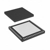


 工商网监
湘ICP备2023018690号
工商网监
湘ICP备2023018690号
