User's Guide
SCAU022A – July 2007 – Revised July 2010
CDCE(L)9xx Performance Evaluation Module
This user’s guide explains how to use the CDCE(L)9xx Performance Evaluation Module (EVM), which is a
generic PCB that can handle all the CDCE(L)9xx devices. The CDCE9xx is soldered on the PCB for best
performance; therefore, it is necessary to specify the desired device when ordering the EVM. The
assembly of the EVM is slightly different for each member of the family. However, the basic functionality
remains the same.
The following EVMs will be available within summer 2007:
• CDCE949EVM
• CDCE925EVM
• CDCE913EVM
CDCEL9xx versions will follow later.
1
2
3
4
5
6
Contents
Block Diagram ............................................................................................................... 2
About the CDCE(L)9xx Clock-Generator Family ........................................................................ 3
QUICK START (USB PLUG 'N' PLAY) .................................................................................. 4
EVM Hardware .............................................................................................................. 5
TI ClockPro™ Programming Software ................................................................................... 8
Bill of Materials and Schematic .......................................................................................... 17
List of Figures
...............................................................
1
CDCE(L)9xx Simplified Block Diagram (Default Setup)
2
CDCEL9xx Printed-Circuit Board ......................................................................................... 3
3
Functional Block Diagram of the CDCE(L)9xx .......................................................................... 4
4
EVM Region Showing SDA Pin and SCL Pin Locations ............................................................... 7
5
TI ClockPro™ Start Window ............................................................................................... 9
6
TI ClockPro™ Devices Search Window
7
TI ClockPro™ Solution Selection Window ............................................................................. 10
8
TI Clock Pro Main View ................................................................................................... 11
9
TI ClockPro™ Direct Register View ..................................................................................... 13
10
TI ClockPro™ Bits Viewer – Bit Contents of the Control Register .................................................. 14
11
TI ClockPro™ Pulling Range Calculator
12
TI ClockPro™ Checksum Calculator .................................................................................... 15
.................................................................................
...............................................................................
2
9
15
List of Tables
1
Bill of Materials............................................................................................................. 17
TI ClockPro, Pro-Clock, ClockPro are trademarks of Texas Instruments.
Bluetooth is a trademark of Bluetooth SIG.
Intel is a trademark of Intel Corporation.
Windows, Excel are trademarks of Microsoft Corporation.
Memory Stick is a trademark of Sony Corporation.
Ethernet is a trademark of Xerox Corporation.
SCAU022A – July 2007 – Revised July 2010
CDCE(L)9xx Performance Evaluation Module
Copyright © 2007–2010, Texas Instruments Incorporated
1
�Block Diagram
1
www.ti.com
Block Diagram
1.8V LDO
(TI)
3.3V LDO
(TI)
J23
(USB Power)
5V
From Notebook / PC
3.3V
3.3V
Output
Supply
Selection
D1
1.8V
Core
Supply
Selection
D2
J41
(S0 HIGH) S0
Y1
22 W
Y2
22 W
Y9
CDCE (L)9XX
Universal Family
Footprint
* set J25 to activate serial interface
22 W
Series terminated outputs
with option for AC coupling
SDA / S1
J33
(SDA active)
SCL / S2
1.8 V
D3
2 way
solder
bridges
USB
SDA
Chip
+
SCL
Peripheral *
(FTDI)
J39
(SCL active)
1.8V
Output
Supply
Selection
Open Jumper
Xin/Clk
Shorted Jumper
(for Default)
VCTR
Xout
VCTR
Y1 crystal
(default)
Figure 1. CDCE(L)9xx Simplified Block Diagram (Default Setup)
1.1
Features
•
•
•
•
•
•
2
Easy-to-use evaluation module for fast prototyping and application evaluation, supporting the entire
clock family.
Easy and fast device programming through TI Pro-Clock™ software
Evaluation of multiple crystals and reference clocks due to flexible input structure
EVM completely USB powered in factory default
Option for USB power and external power supply
No need for programming or notebook/PC connection
CDCE(L)9xx Performance Evaluation Module
Copyright © 2007–2010, Texas Instruments Incorporated
SCAU022A – July 2007 – Revised July 2010
�About the CDCE(L)9xx Clock-Generator Family
www.ti.com
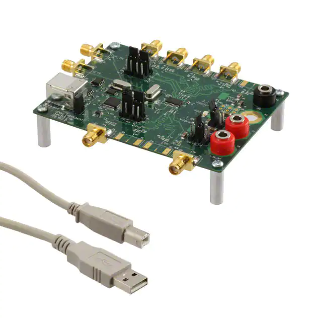
Figure 2. CDCEL9xx Printed-Circuit Board
1.2
Related Documentation From Texas Instruments
•
•
•
•
•
1.3
CDCE949, CDCE(L)949, Programmable, 4-PLL VCXO Clock Synthesizer With 1.8-V and 3.3-V
Input/Outputs data sheet (SCAS844)
CDCE(L)937 data sheet (Unpublished)
CDCE(L)925 data sheet (Unpublished)
CDCE(L)913 data sheet (Unpublished)
VCXO Application Guidelines for CDCE(L)9xx Family application report (SCAA085)
If You Need Assistance
If you need assistance with this device, send an e-mail to clocks_apps@list.ti.com.
2
About the CDCE(L)9xx Clock-Generator Family
The CDCE9xx and CDCEL9xx are a family of modular PLL-based, low-cost, high-performance,
programmable clock synthesizers, multipliers, and dividers. They generate from 3 (1-PLL) up to 9 (4-PLL)
output clocks from a single input frequency. A crystal or LVCMOS clock signal is possible as the reference
clock. VCXO functionality is built into every member of the CDCE9xx device family, which allows
synchronizing the output frequency to an external control signal, e.g., a PWM signal.
A deep M/N divider ratio allows the generation of zero ppm audio/video, networking (WLAN, Bluetooth™,
Ethernet™, GPS), or interface (USB, IEEE1394, Memory Stick™) clocks from a 27-MHz reference input
frequency, for example.
SCAU022A – July 2007 – Revised July 2010
CDCE(L)9xx Performance Evaluation Module
Copyright © 2007–2010, Texas Instruments Incorporated
3
�QUICK START (USB PLUG 'N' PLAY)
www.ti.com
An inbuilt EEPROM cuts off the need for reprogramming the CDCE(L)9xx in a certain application, but
reprogramming is still possible with a 2-wire serial interface. Based on the PLL frequency and the divider
settings, the internal loop filter components are automatically adjusted to achieve high stability and
optimized jitter transfer characteristic of each PLL. Three, free programmable control inputs, S0, S1, and
S2, can be used to select different frequencies, or change SSC setting for lowering EMI, or other control
features like outputs disable to low, outputs 3-state, power down, PLL bypass, etc.
The device has separate output supply pins, VDDOUT, which is 1.8 V for CDCEL9xx and to 2.5 V to 3.3 V
for CDCE9xx.
The following is an overview of the devices of the CDCE(L)9xx family:
• CDCE949/CDCEL949: 4-PLL, 9 outputs, fmax = 230 MHz, industrial temperature
• CDCE937/CDCEL937: 3-PLL, 7 outputs, fmax = 230 MHz, industrial temperature
• CDCE925/CDCEL925: 2-PLL, 5 outputs, fmax = 230 MHz, industrial temperature
• CDCE913/CDCEL913: 1-PLL, 3 outputs, fmax = 230 MHz, industrial temperature
range,
range,
range,
range,
24
20
16
14
pins
pins
pins
pins
Figure 3. Functional Block Diagram of the CDCE(L)9xx
3
QUICK START (USB PLUG 'N' PLAY)
The following steps allow the user to get started quickly with the EVM.
1. Connect the EVM with the PC with a 2.0 USB cable.
2. Install the driver software using the provided CD-ROM.
3. The EVM is now running and completely powered through USB. Verify it by checking any of the
4
CDCE(L)9xx Performance Evaluation Module
Copyright © 2007–2010, Texas Instruments Incorporated
SCAU022A – July 2007 – Revised July 2010
�EVM Hardware
www.ti.com
outputs available at the SMA connectors.
4. Programming the device is also possible using the TI Pro-Clock™ dedicated software (see section
4.2).
4
EVM Hardware
4.1
Hardware Configuration
This section gives an extended description of the board hardware, providing the user with a
comprehensive overview of its configuration. Detailed information regarding onboard jumpers,
solder-bridges, and communication interface (I2C/SMBus) is also provided, allowing the user to change the
setup and play around according to his needs and wishes.
4.1.1
Power Supply
Power for the EVM can be supplied fully not only via the USB but also through a stabilized external power
supply. The following paragraphs describe how to set the board jumpers for both cases. Depending on the
device the user is dealing with (CDCE9xx or CDCEL9xx), a guideline of the jumper’s setup for the output
stage is given.
NOTE: All EVMs are delivered with USB power supply as default.
4.1.1.1
External Power Supply
In order for the board to be supplied with an external power supply generator, follow the instructions
regarding the jumpers’ setup for both the device core and the output stage. The latter depends on the type
of device (CDCE9xx or CDCEL9xx).
Core Supply Voltage
• Insert jumper J47 (leave jumper J46 open).
• Connect the positive pole of the external power supply to P1 and the negative pole to P2 (ground).
Voltage ranges between 1.7 V and 1.9 V (nominal 1.8 V).
• Insert jumpers J23 and J25 and plug in the USB cable (use a 2.0 USB male B termination). Even
though externally supplied, the board needs this connection to allow the programming of the device.
Output Stage Supply Voltage (Either 3.3 V or 1.8 V)
a) CDCE9XX → VDDOUT = 3.3 V
• Insert jumper J44 (leave J43 and J45 open).
• Connect the positive pole of the external power supply to P3 and the negative pole to P2 (ground).
Voltage ranges between 3 V and 3.6 V (nominal 3.3 V).
NOTE: J45→ use this jumper to ground Vddout. In this way, the default functionality for the SDA/S1
and SCL/S2 pins is recalled, and the device can be reprogrammed even though these pins
were set to control pins (S1 and S2). Besides, the device default address is also recalled.
Set J39 and J33 for SDA and SCL to reprogram the device (leave J32, J34, J38, and J40
open).
b) CDCEL9XX → VDDOUT=1.8 V
• Insert jumper J50 (leave jumpers J49 and J51 open).
• Connect the positive pole of the external power supply to P4 and the negative pole to P2 (ground).
Voltage ranges between 1.7 V and 1.9 V (nominal 1.8 V).
SCAU022A – July 2007 – Revised July 2010
CDCE(L)9xx Performance Evaluation Module
Copyright © 2007–2010, Texas Instruments Incorporated
5
�EVM Hardware
www.ti.com
NOTE: J51→ use this jumper to ground Vddout. In this way, the default functionality for the SDA/S1
and SCL/S2 pins is recalled, and the device can be reprogrammed even though these pins
were set to control pins (S1 and S2). Besides, the device default address is also recalled.
Set J39 and J33 for SDA and SCL to reprogram the device (leave J32, J34, J38, and J40
open).
4.1.1.2
USB Power Supply
In order for the board to be fully supplied via USB, follow the instructions regarding the jumpers’ setup for
both the device core and the output stage. The latter depends on the type of device (CDCE9xx or
CDCEL9xx).
NOTE:
All EVMs are delivered with the USB power supply as default.
Core Supply Voltage
• Insert jumper J46 (leave jumper J47 open).
• Insert jumper J23 and J25, and plug in the USB cable (use a 2.0 USB male B termination).
Output Stage Supply Voltage (Either 3.3 V or 1.8 V)
a) CDCE9XX → VDDOUT = 3.3 V
• Insert jumper J43 (leave J44 and J45 open).
NOTE: J45 → use this jumper to ground Vddout. . In this way, the default functionality for the
SDA/S1 and SCL/S2 pins is recalled and the device can be reprogrammed even though
these pins were set to control pins (S1 and S2). Besides, the device default address is also
recalled. Set J39 and J33 for SDA and SCL to reprogram the device (leave J32, J34, J38,
and J40 open).
b) CDCEL9XX → VDDOUT = 1.8 V
• Insert jumper J49 (leave jumper J50 and J51 open).
NOTE: J51→ use this jumper to ground Vddout. In this way, the default functionality for the SDA/S1
and SCL/S2 pins is recalled and the device can be reprogrammed even though these pins
were set to control pins (S1 and S2). Besides, the device default address is also recalled.
Set J39 and J33 for SDA and SCL to reprogram the device (leave J32, J34, J38, and J40
open).
4.1.2
Programming Interfaces
The device supports nonvolatile EEPROM programming for easy customized applications. Although preset
to a factory default configuration (see the relevant data sheet), it can be reprogrammed to a different
application configuration. All device settings are programmable through the SDA/SCL bus, a 2-wire serial
interface that works according to the I2C standard specification.
Three, free programmable control inputs, S0, S1, and S2, can be used to select different frequencies, or
change the SSC setting for lowering EMI, or other control features like, outputs disable to low, outputs
3-state, power down, PLL bypass, etc.
The device can be programmed externally in two ways:
1. Via the USB cable connected to the PC and to the EVM (in this mode, J39 and J33 are set). TI
Pro-Clock™ software (see section 4) supports the device programming.
2. By an external pattern generator connected to J39 (clock) and J33 (data).
The EVM also offers the opportunity to change the configuration setting of the device by switching the set
of S0, S1, and S2 (see the relevant device data sheet). This can be done by simply inserting and
removing the jumpers by the following description:
6
CDCE(L)9xx Performance Evaluation Module
Copyright © 2007–2010, Texas Instruments Incorporated
SCAU022A – July 2007 – Revised July 2010
�EVM Hardware
www.ti.com
•
•
•
4.1.3
S0: Insert J41 to set it HIGH; insert J42 to set it LOW.
S1: Insert J32 to set it HIGH; insert J34 to set it LOW (always leave J33 open).
S2: Insert J38 to set it HIGH; insert J40 to set it LOW (always leave J39 open).
Pass Programming Through
This option allows the device to be programmed on your own board, through the CDCE(L)9xx EVM, by
simply connecting the SDA/SCL available pins to your programming interface.
• Insert jumper J23 and J25 and plug in the USB cable (use a 2.0 USB male B termination).
• Connect the SDA wire and the SCL wire as shown in Figure 4. This is a zoomed view of the EVM
region where the jumpers 32, 33, 34, 38, 39, and 40 are placed.
SDA pin:
Connect
terminal’s
wire here
SCL pin:
Connect
terminal’s
wire here
Figure 4. EVM Region Showing SDA Pin and SCL Pin Locations
•
•
4.1.4
Connect the other SDA and SCL wire terminals to your programming interface.
The setup is ready; communication with the customer onboard device is now possible.
Input
The CDCE(L)9xx can be driven either from a crystal or from an LVCMOS input signal. If a crystal is
connected, the CDCE(L)9xx can act as a crystal oscillator or as a VCXO with integrated PLLs. Two crystal
footprints allow connecting a smaller 4-pin crystal and a larger 2-pin crystal. This eases the evaluation of
different crystals with different footprint and size. The 2-pin crystal (Y1) on the EVM top side is used as
default.
NOTE: The EVM default is a crystal oscillator with 2-pin crystal (Y1). (See Figure 1)
4.1.4.1
Crystal or VCXO
The following steps are necessary to use the EVM with a crystal or VCXO as reference:
1. General 2-pin crystal or VCXO setup
The 2-pin crystal footprint allows evaluating crystals with a larger size. Larger size crystals usually offer
a wider tuning range for the VCXO functionality.
SCAU022A – July 2007 – Revised July 2010
CDCE(L)9xx Performance Evaluation Module
Copyright © 2007–2010, Texas Instruments Incorporated
7
�TI ClockPro™ Programming Software
www.ti.com
(a) Short pin 1 and 2 of J52.
(b) Short pin 3 and 2 of J4.
(c) Ensure that R2 and R4 are not installed.
(d) Ensure that C1 and C2 are not installed.
2. General 4-pin crystal or VCXO setup
The 4-pin crystal footprint is a universal footprint that allows evaluating different smaller 2- and 4-pin
crystals. Smaller crystals are beneficial, if a simple crystal oscillator without VCXO functionality is
needed. Smaller crystals are usually cheaper and need less board space.
(a) Short pin 2 and 4 of J52.
(b) Short pin 1 and 2 of J4.
(c) Ensure that R2 and R4 are not installed.
(d) Ensure that C1 and C 2 are not installed.
3. VCXO setup
Because the device has an integrated VCXO, it is possible to verify its functionality (pull-ability) using
the VCTR connector (J30). Install an appropriate resistor R6 to adjust the voltage level according to
the need (R5, R6 work together as a voltage divider).
(a) Assemble R5 and C31 (low pass for VCXO) as needed.
(b) R6 and R5 can be used to create a voltage divider for shifting down the control voltage.
(c) Connect the control voltage to J30.
4.1.4.2
LVCMOS
CLK_IN is available via jumper J2 for driving the CDCE(L)9xx with an LVCMOS input. In this case, R2 and
R4 can be installed on the EVM. Assembling R2 and R4 with 100 Ω each matches the 50-Ω termination of
a signal generator. C4 permits AC coupling to the external signal source. Ensure that the jumper J52 is
shorted between pin 3 and pin 2, which connects J2 (CLK_IN) with pin 1 (CLK) of the device.
4.1.5
LVCMOS Output
The CDCE(L)9xx can drive from three LVCMOS outputs (CDCE(L)913) up to nine LVCMOS outputs
(CDCE(L)949). Most of them are accessible via SMA connectors. All outputs are series terminated with a
22-Ω resistor in series to the output.
For each output routed on the EVM, it is possible to AC-couple it (i.e., Y1). Depending on the application
requirements, install the resistors for adjusting the DC level (for Y1 → R74 and R76). Power this voltage
divider with the wanted voltage supply (either 1.8 V or 3.3 V) by using the dedicated jumper (for Y1 →
J12), and install a capacitor (for Y1 → C23) with a value between 10 nF and 100 nF.
4.1.5.1
Y4 Output
The pin 7 corresponds to the output Y4, and this is valid for the device CDCE(L)925, CDCE(L)937, and
CDCE(L)949. For the CDCE(L)913, this pin serves as VDDOUT. J6, J7, and C28 are set accordingly.
5
TI ClockPro™ Programming Software
The TI ClockPro™ design tool is the evaluation software for the CDCE(L)949, CDCE(L)937, CDCE(L)925,
and CDCE(L)913 clocking family.
The software runs under Windows™ 98, NT, 2000, XP, and Vista. A quick installation is required prior to
use.
After the loading screen, the start window is shown (Figure 5). This initial window called TI ClockPro™
Wizard recommends devices based on the frequencies and conditions required by the user. It is also
possible to skip this window, going directly to the Devices Search Window (Figure 6). The Devices Search
Window allows the user to select the EVM to work with or go to local mode. After pressing OK, the user is
directed to the Main View Window (Figure 8), that offers the capabilities of communicating with the device,
creating new setups, and loading setups in the device. Under the Tools menu option, other views [Direct
register view (Figure 9), the bits View (Figure 10)] and utilities [Pulling Range Tool (Figure 11) and
Checksum Calculator (Figure 12)] can be accessed.
8
CDCE(L)9xx Performance Evaluation Module
Copyright © 2007–2010, Texas Instruments Incorporated
SCAU022A – July 2007 – Revised July 2010
�TI ClockPro™ Programming Software
www.ti.com
5.1
Loading and Saving a Setup
Saving and loading the setup of the CDCE(L)9xx software can be done in several different ways.
Click File, and select one of the following options to save or load the current setup.
1. Load Setup/Save Setup — loads/saves the setup from/to an encrypted file
2. Load *.txt/Save *.txt — loads/saves the setup from/to a text file. Use this format to view the setup later
with a text editor.
3. Load *.csv/Save *.csv — loads/saves the setup from/to a comma-delimited file. Use this format to view
the setup later with Microsoft™ Excel™.
4. Load Intel™ Hex*.hex/Save Intel Hex*.hex — loads/saves the setup from/to hexadecimal object file
format. Usually, programmers can directly read-in this file format.
5. Configuration Code Release Sheet — use this option to order factory-programmed EEPROM specials
of the CDCE(L)9xx. Contact your regional TI marketing or sales representative for further information.
(1)
(2)
(3)
(6)
(4)
(7)
(5)
Figure 5. TI ClockPro™ Start Window
1.
2.
3.
4.
Setup Name. Customized level that refers to the set of solutions that the wizard can generate
fin(MHz). User's input frequency in MHz
No of Outputs. Number of outputs to generate out of the input frequency introduced in (2)
Spread Spectrum. If the outputs require spread spectrum, checking this option allows the customer to
introduce the SSC settings per output.
5. Output conditions. This group of controls allows the user to introduce output frequency in MHz and if
required SSC Conditions (offset and percentage)
6. Skip button directs the user to device selection window (Figure 6)
7. Generate Setup button recommends devices that generate out of fin the fout conditions introduced by
the user. The solutions are listed in the window (Figure 7)
(1)
(3)
(2)
(4)
Figure 6. TI ClockPro™ Devices Search Window
1. Select Device chooses the device to work with. When an EVM is connected, it appears as a first
option. Nonconnected options (local mode) are also available.
2. It is green when an EVM is connected. It is black when working in local mode (no data is transferred to
the EVM).
3. OK button directs to the Main View (Figure 8), or if Generation Setup button was pressed on the
SCAU022A – July 2007 – Revised July 2010
CDCE(L)9xx Performance Evaluation Module
Copyright © 2007–2010, Texas Instruments Incorporated
9
�TI ClockPro™ Programming Software
www.ti.com
Wizard Window, it directs to the Solution Selection Window (Figure 7).
4. Refresh updates the choices in (1).
(1)
(2)
(3)
(4)
(5)
Figure 7. TI ClockPro™ Solution Selection Window
1. Solution Selection selects the solution to view when pressing the button View Setup (3). Many
different solutions can be generated by different combinations of the devices and the input stage.
2. Device Selection chooses the initial setup to load in the Main View (Figure 8).
3. View Setup loads the selected device for the selected solution in the Main View (Figure 8).
4. Skip button skips loading a solution showing the Main View (Figure 8).
5. Back button goes back to the Wizard View (Figure 5).
10
CDCE(L)9xx Performance Evaluation Module
Copyright © 2007–2010, Texas Instruments Incorporated
SCAU022A – July 2007 – Revised July 2010
�TI ClockPro™ Programming Software
www.ti.com
(1)
(2)
(3)
(4)
(19)
(17)
(18)
(5)
(6)
(7)
(8)
(9)
(10)
(11)
(12)
(13)
(14)
(15)
(16)
Figure 8. TI Clock Pro Main View
1. Main Menu bar with three menu options. File menu option supports loading and saving of files (.isf,
.csv, .txt, .hex, .configuration code release sheet) and exiting the program. With the Through the Tools
menu, the following tools can be accessed: Bit Viewer, Pulling Range Tool, Check sum calculator,
Direct Register View, and Wizard View. Also via the Tools menu, the device can be reset to default
(menu option: Go Default) and the current setup can be written to EEPROM (menu option: Write to
EEPROM). The Help menu has a link to the About window that contains information about the version
number of the current software.
2. The Connection indicator is Green when the device selected in (12) is a device in a performance EVM.
When it is black, the device selected in (12) is working in local mode.
3. If connected, the Write to Device button writes all the displayed contents in the Main View (Figure 8)
and the Direct Register View (Figure 9) in the device's control register.
4. If connected, the Read from Device button reads all the contents of the device's control register in the
Main View (Figure 8) and in the Direct Register View (Figure 9).
5. If connected, the Write to EEPROM button writes all the displayed contents in the Main View (Figure 8)
and in the Direct Register View (Figure 9) in the device's EEPROM.
6. Bit Viewer button. When it is pressed, it shows the Bits Viewer Tool (Figure 10).
7. Direct Reg. button. When it is pressed, it shows the Direct Register View (Figure 9).
8. Wizard button. When it is pressed, it shows the Wizard View (Figure 5).
9. Go default button. When it is pressed, it loads the default setup as per device selected in (12).
10. Checksum button. When it is pressed, it shows the Checksum Calculator Tool (Figure 12).
11. Control Line Selection. This displays the control pins settings linked to the active setup. This control
does not change the control pins voltages in the performance EVM. In order to ensure that the active
setup in the performance EVM is the same as the setup displayed in this view, ensure that (11) and
the jumpers in the EVM are set to the same values.
The use of S1 and S2 depends on SPICON, which decides if S1 and S2 are used as control pins or as
SCAU022A – July 2007 – Revised July 2010
CDCE(L)9xx Performance Evaluation Module
Copyright © 2007–2010, Texas Instruments Incorporated
11
�TI ClockPro™ Programming Software
www.ti.com
serial interface pins.
If SPICON is logic 0, the serial control interface is enabled. In this case, S1 is used as SDA, and S2 is
used as SCL. For the internal logic, S1 and S2 are considered to be "0". This means that either control
pin selection "000" or "001" is active, depending on the logic level at S0.
If SPICON is logic 1, S1 and S2 are used as control pins, and the serial interface is disabled. The
internal logic S1 and S2 are considered to be 0 or 1, according to the logic level that is connected to
these pins. In this case, up to eight different device setups can be selected through S2, S1, and S0.
The SPICON configuration is possible in the generic control register (GCR). For the EVM default
configuration, SPICON is logic 0. This results in S0 = 1, S1 = 0, S2 = 0, according to the default
jumper setting on the EVM.
If Vdd is connected and Vddout is forced to GND, S1, and S2 act as serial interface pins – even if
SPICON is logic 1. This allows reprogramming the device, if the control pin functionality is enabled. For
more information, see the CDCE(L)9xx data sheet.
12. Select Device chooses the device where all the actions are performed.
13. Refresh devices button. When pressed, it looks for the EVMs connected.
14. Solution selection shows the solution generated by the Wizard View (Figure 5).
15. List of devices shows those devices that are part of the solution selected in (14).
16. Select button. When it is pressed, the selected device in (15) are loaded in the program.
17. Life update. When checked and the device selected, all changes in the setup (Wizard View (Figure 8)
or Direct Register View (Figure 9) are automatically written to the control register.
18. Limited Ranges Mode. When checked when a setup is loaded or a change is performed in the setup,
the change is ensured to be within the specifications. If not checked, the verification of settings within
specifications is skipped.
19. Reset PPM Reference. The ppm is calculated with respect to the requested output frequency in the
Wizard View. After this button is pressed, the ppm is calculated with respect to the output frequency
when that occurred.
20. Current status
12
CDCE(L)9xx Performance Evaluation Module
Copyright © 2007–2010, Texas Instruments Incorporated
SCAU022A – July 2007 – Revised July 2010
�TI ClockPro™ Programming Software
www.ti.com
(1)
(2)
(3)
(4)
(5)
(6)
(7)
(8)
(9)
(10)
Figure 9. TI ClockPro™ Direct Register View
1. Main Menu bar with three menu options as per Main View Menu Bar (Figure 8)
2. The Connection indicator is green when the device selected in (7) is a device in a performance EVM.
When black, the device selected in (7) is working in local mode.
3. If connected, the Write to Device button writes all the displayed contents in the Main View (Figure 8)
and in the Direct Register View (Figure 9) in the device's control register.
4. If connected, the Read from Device button reads all the contents of the device's control register in the
Main View (Figure 8) and in the Direct Register View (Figure 9).
5. If connected, the Write to EEPROM button writes all the displayed contents in the Main View (Figure 8)
and in the Direct Register View (Figure 9) in the device's EEPROM.
6. Control Line Selection. This shows the control pins settings linked to the active setup. This control
does not change the control pins voltages in the performance EVM. In order to ensure that the active
setup in the performance EVM is the same as the setup displayed in this view, ensure that (6) and the
jumpers in the EVM are set to the same values.
7. Select Device chooses the device where all the actions are performed.
8. Refresh devices button. When pressed, it looks for EVMs connected.
9. Live update. When checked and the device is selected, all changes in the setup (Wizard View,
Figure 8, or Direct Register View, Figure 9, are automatically written to the control register.
10. Limited Ranges Mode. When checked and a setup is loaded or a change is performed in the setup,
the change is ensured to be within the specifications. If not checked, the verification of settings within
specifications is skipped.
SCAU022A – July 2007 – Revised July 2010
CDCE(L)9xx Performance Evaluation Module
Copyright © 2007–2010, Texas Instruments Incorporated
13
�TI ClockPro™ Programming Software
www.ti.com
Figure 10. TI ClockPro™ Bits Viewer – Bit Contents of the Control Register
14
CDCE(L)9xx Performance Evaluation Module
Copyright © 2007–2010, Texas Instruments Incorporated
SCAU022A – July 2007 – Revised July 2010
�TI ClockPro™ Programming Software
www.ti.com
Figure 11. TI ClockPro™ Pulling Range Calculator
Figure 12. TI ClockPro™ Checksum Calculator
5.2
Software Installation
Use the following steps to install the CDCE(L)9xx evaluation software:
1. Insert CDCE(L)9xx EVM compact disc.
2. Click on setup.exe to install TI Pro Clock software.
→ Folder: TI-Pro-Clock
3. Reboot your computer
4. Run software from desktop Ti ProClock™ icon.
SCAU022A – July 2007 – Revised July 2010
CDCE(L)9xx Performance Evaluation Module
Copyright © 2007–2010, Texas Instruments Incorporated
15
�TI ClockPro™ Programming Software
www.ti.com
or
Start → Programs → Texas Instruments → TI Pro Clock
Three different drivers are available.
1. Windows 98 and Windows ME in folder w-98-ME
2. Windows XP, Windows Vista, Windows Server 2003, Windows 2000 in folder w-xp-vista-server-2000
Windows XP x64,
3. Windows Vista x64 and Windows Sever 2003 x64 in folder w-xp-vista-server-64
16
CDCE(L)9xx Performance Evaluation Module
Copyright © 2007–2010, Texas Instruments Incorporated
SCAU022A – July 2007 – Revised July 2010
�Bill of Materials and Schematic
www.ti.com
6
Bill of Materials and Schematic
6.1
Bill of Materials
Table 1. Bill of Materials
Item
Qty
RefDes
Value
1
0
C1, C2
10 pF
Manufacturer
Part Number
NU
2
0
C3, C9
NU
NU
3
9
C11-C15, C17,
C19, C21, C23
0Ω
Panasonic - ECG
ERJ-2GE0R00X
4
8
C4, C5, C7, C26,
C37,C41,
C53,C67
10 nF
Panasonic - ECG
ECJ-0EB1E103K
5
3
C6, C8, C61
1 nF
Panasonic - ECG
ECJ-0EB1E102K
6
8
C16, C20,
C39,C50,
C62-C65
4.7 mF
Panasonic - ECG
ECJ-3YB1C475M
7
5
C18, C24, C51,
C60,C66
1 mF
Panasonic - ECG
ECJ-0EB1A105M
8
0
C28
10 nF
Panasonic - ECG
ECJ-0EB1E103K
9
18
C29, C31-C33,
C36, C40,
C44-C48,
C54-C59, C68
0.1 mF
Panasonic - ECG
ECJ-0EB1A104K
10
1
C35
10 mF
Panasonic - ECG
ECJ-3YB1A106M
11
1
C38
47 pF
AVX Corporation
04025A470JAT2A
12
2
C42, C43
27 pF
AVX Corporation
04025A270JAT2A
13
2
C49, C52
33 nF
AVX Corporation
0402YD333KAT2A
14
1
C70
220 pF
Panasonic
ECJ-0EB1E221K
15
2
D1, D2
Red
Lumex Opto/Components Inc
SML-LX1206SR-TR
16
0
D3
Red
Conn USB
Typ B Fem
Mill-Max
897-30-004-90-000
NU
17
1
J1
18
2
J2, J30
SMA
Johnson Comp
142-0701-851
Panasonic - ECG
ERJ-2GE0R00X
19
3
J4, J24, J29
SMD3P_BRI
DGE
20
3
J6-J8
SMD3P_BRI
DGE
Panasonic - ECG
ERJ-2GE0R00X
21
0
J10-J15,J31, J36,
J37
SMD3P_BRI
DGE
Panasonic - ECG
ERJ-2GE0R00X
22
0
J16
Y5
23
1
J17
Y6
Johnson Comp
142-0701-851
24
0
J18
Y7
25
0
J19
Y8
26
1
J20
Y9
Johnson Comp
142-0701-851
27
1
J21
Y2
Johnson Comp
142-0701-851
28
1
J22
Y3
Johnson Comp
142-0701-851
29
16
J23, J25, J26,
J32-J34, J38-J47
Jumper
Header 2 pos, 0.100 ctr
30
0
J49-J51
Jumper
NU
31
1
J27
Y4
Johnson Comp
142-0701-851
32
1
J35
Y1
Johnson Comp
142-0701-851
J52
SMD4P_BRI
DGE
Panasonic - ECG
ERJ-2GE0R00X
33
1
SCAU022A – July 2007 – Revised July 2010
NU
NU
NU
CDCE(L)9xx Performance Evaluation Module
Copyright © 2007–2010, Texas Instruments Incorporated
17
�Bill of Materials and Schematic
www.ti.com
Table 1. Bill of Materials (continued)
Item
18
Qty
RefDes
Value
Manufacturer
Part Number
Murata Electronics
BLM21AG102SN1D
34
2
L4, L5
1k @ 100
MHz
35
3
L6-L8
50 Ω @ 100
MHz
Murata Electronics
BLM31PG500SN1L
36
1
P1
1.8 V
SPC Technologies
845R
37
1
P2
GND
SPC Technologies
845R
38
1
P3
3.3V_OUT
SPC Technologies
845R
39
0
P4
40
0
R1
41
0
R2, R4
42
0
R3
43
2
R5, R54
200k
44
0
R6
NU
45
5
R7, R8, R26,
R59, R68
1k
46
0
R9
1M
Panasonic - ECG
ERJ-2RKF1004X
47
1
R16
470
Yageo Corporation
RC0402FR-07470RL
48
1
R19
1.5k
Panasonic - ECG
ERJ-2GEJ152X
49
0
R22, R25, R28,
R32, R34, R35,
R37, R38,
R40,R41, R43,
R53, R60, R62,
R64,R66, R74,
R76
Panasonic - ECG
ERJ-2RKF1000X
50
9
R23, R29, R33,
R36, R39, R42,
R61, R65, R75
22 Ω
Panasonic - ECG
ERJ-2GEJ220X
51
1
R24
2.2k
Panasonic - ECG
ERJ-2GEJ222X
52
1
R27
10k
Panasonic - ECG
ERJ-2GEJ103X
53
2
R30, R31
26.7
Panasonic - ECG
ERJ-2RKF26R7X
54
9
R48-R52, R63,
R67, R71, R72
0Ω
Panasonic - ECG
ERJ-2GE0R00X
55
2
R55, R56
5.6k
Panasonic - ECG
ERJ-2GEJ562X
56
2
R57, R58
10k
Panasonic - ECG
ERJ-2GEJ103X
57
1
R69
160
Yageo Corporation
9C04021A1600JLHF3
58
2
R70, R73
10
Panasonic - ECG
ERJ-2RKF10R0X
59
1
U13
TPS77533D
TI
TPS77533D
93C66B/TSS
OP
MicroChip
93C66B
NU
1M
Panasonic - ECG
ERJ-2RKF1004X
Panasonic - ECG
ERJ-2GEJ101X
Panasonic - ECG
ERJ-2GEJ204X
NU
NU
Panasonic - ECG
ERJ-2GEJ102X
60
1
U16
61
1
U17
FT2232
FTDI
FT2232L
62
1
U18
CDCE949
TI
CDCE949PW
63
1
U20
TPS77518D
TI
TPS77518D
64
1
U21
PCA9306
TI
PCA9306DCU
Crystal 27
MHz, 10-pF
Load
KDS
SMD-49 (PN ZD02580)
ECS Inc
ECS-60-32-5PDN-TR
65
1
Y1
66
1
Y2
6 MHz
67
0
Y3
Variable
Crystal
68
4
Screw
H781-ND
Building Fasteners
PMS 440 0038 PH
69
4
Standoff
3481K-ND
Keystone Electronics
3481
Variable
CDCE(L)9xx Performance Evaluation Module
Copyright © 2007–2010, Texas Instruments Incorporated
SCAU022A – July 2007 – Revised July 2010
�Bill of Materials and Schematic
www.ti.com
Table 1. Bill of Materials (continued)
Item
70
6.2
Qty
RefDes
Value
Manufacturer
Part Number
6
2-Pin
Jumper/Short for
J23, J25, J39,
J41, J43, J46
AMP Novo
Shunt
Tyco Electronics
0-0881545-1
Schematic
The CDCE9xx EVM schematic is appended to this page.
SCAU022A – July 2007 – Revised July 2010
CDCE(L)9xx Performance Evaluation Module
Copyright © 2007–2010, Texas Instruments Incorporated
19
�3
2
1
C2
XinO
10 pF
Do Not Install
Do Not Install
R4
100
Xin2
2
2
27 MHz
2
C1
10 pF
Do Not Install
1
10nF
CLKIN_SMA
S0
1.8V
Vctr
2
2
C32
100nF
R5
200k
Y5
3.3V_OUT
Default: Short 2 & 3 on J8
C31 1.8V_OUT
0.1uF
Xin/Clk Xout
S0
S1/SDA
VDD S2/SCL
Vctr
Y1
GND
GND
Vddout
Y2
Y4
Y3
Y5
Vddout
GND
Y6
Vddout
Y7
Y8
GND
Y9
VDD
3
1
1
Y1
Y2
Y3
Y6
CDCE949
Y9
Y7
C29
100nF
3
1
C33
100nF
3.3V_OUT
Default: Short 2 & 3 on J7
J29
1.8V
B
1
J24
1.8V_OUT
Default: Insert Jumper of J41
2
JUMPER J38
2
1
S0
S2/SCL
JUMPER J39
2
1
J32 JUMPER
1
2
2
2
Default: Insert Jumper of J33
1
1
JUMPER J40
R68
1k
Default: Short 2 & 3 on J29
S1/SDA
SCL
JUMPER J42
2
1
1.8V_OUT 3.3V_OUT
3.3V_OUT
Default: Short 2 & 3 on J24
J33 JUMPER
1
2
SDA
3
1
2
1
R8
1k
JUMPER J41
2
1
C
2
1
1.8V_OUT
R7
1k
B
S1/SDA
S2/SCL
J7
1.8V
1.8V
24
23
22
21
20
19
18
17
16
15
14
13
Y8
2
R6
N.U.
Do Not Install
Y4
2
Do Not Install
C28
100nF
2
1
J6
3
3
1
J30
1 2
SMA
1
J8
1
3
Default: Short 2 & 3 on
50
Do Not Install
C
1
2
3
4
J65
6
7
8
9
10
11
12
2
2
R3
2
Do Not Install
Do Not Install
C4
1
1
SMA
D
Xin2
J2
1CLK_SMA
2
C3
NU
Do Not Install
3
3
U18
C9
NU
Do Not Install
2
1
XinO
Do Not Install
4
Do Not Install
Y3
J4
2
1
Y1
XOUT1
1
1
2
3
4
R2
100
Do Not Install
R9
1M
1
2
2
2
XOUT1
1
1
J52
XOUT1
R1 1M Do Not Install
1
2
D
Default: Short 3 & 2 on J4
Default: Short 2 & 11.8Von J52
3
4
2
5
2
J34 JUMPER
Default: Insert Jumper of J39
A
1
2
A
Title
R59
1k
Jupiter Evaluation Module
1
Size
Document Number
A
Date:
5
4
3
Rev
B1
CDCE949 EVM
Wednesday, May 16, 2007
2
Sheet
1
of
1
4
�5
4
3
2
1
1.8V_OUT
D
J14
D
Default: Don't Connect any resistors in between 1 & 2 and 3 & 2
3.3V_OUT 3
Do Not Install
100
R22
22 ohm
2
C11 10nF
1
2
1
0 ohm
2
JY5
1
2
Do Not Install
100
R25
2
Default: Don't
install the cap.
Bridge with 0 Ohm
resistor
R48
J16
GND
1.8V_OUT
GND
J31
Default: Don't Connect any resistors in between 1 & 2 and 3 & 2
1
2
3.3V_OUT 3
Do Not Install
100
R32
Y6
C
C12 10nF
1
2
1.8V_OUT
J15
JY6
1
2
Do Not Install
100
R34
J17
C
GND
GND
2
Default: Don't
install the cap.
Bridge with 0 Ohm
resistor
Y6
0 ohm
R49
1
2
12
Y6
22 ohm
R33
1
2
3
R23
Default: Don't install SMA
1
1
12
Y5
Y5
Y5
3
2
1
1
Default: Don't Connect any resistors in between 1 & 2 and 3 & 2
3.3V_OUT 3
Do Not Install
100
R35
Y7
C13 10nF
1
2
1
12
Y7
22 ohm
R36
1
2
Y7
0 ohm
2
JY7
2
Default: Don't install SMA
1
2
Do Not Install
100
R37
Default: Don't
install the cap.
Bridge with 0 Ohm
resistor
R50
3
2
1
1
J18
GND
GND
1.8V_OUT
J36
Default: Don't Connect any resistors in between 1 & 2 and 3 & 2
1
B
3.3V_OUT 3
Y8
1
C14 10nF
1
2
Default: Don't
install the cap.
Bridge with 0 Ohm
resistor
1.8V_OUT
J37
R40
Do Not Install
100
1
R51
Y8
0 ohm
2
JY8
1
2
Do Not Install
100
J19
GND
Default: Don't install SMA
2
Y8
22 ohm
2
12
R38
R39
3
2
1
B
GND
Default: Don't Connect any resistors in between 1 & 2 and 3 & 2
3.3V_OUT 3
R41
Do Not Install
100
0 ohm
R52
1
2
12
Y9
Y9
C15 10nF
1
2
R43
Default: Don't
install the cap.
Bridge with 0 Ohm
resistor
2
A
22 ohm
R42
1
2
Y9
3
2
1
1
JY9
1
2
A
Do Not Install
100
J20
GND
GND
Title
Jupiter Evaluation Module
Size
B
Date:
5
4
3
2
Document Number
Rev
B1
CDCE949 EVM
Monday, April 16, 2007
Sheet
1
2
of
4
�5
4
3
2
1
1.8V_OUT
2
D
Do Not Install
100
R74
1
R75
22 ohm
2
C23 10nF
1
2
0 ohm
2
JY1
1
2
J35
GND
GND
2
J13
R63
Do Not Install
100
R76
1.8V_OUT
Default: Don't Connect any resistors in between 1 & 2 and 3 & 2
2
1
1
1
12
Y1
Y1
Y1
3
D
J12 Default: Don't Connect any resistors in between 1 & 2 and 3 & 2
1
Default: Don't
1
install the cap.
Bridge with 0 Ohm
3.3V_OUT 3
resistor
R28
Y2
Y2
1
R29
22 ohm
2
C17 10nF
1
2
1
12
C
Do Not Install
100
R53
2
Default: Don't
install the cap.
Bridge with 0 Ohm
resistor
R67
Y2
3
3.3V_OUT 3
0 ohm
2
C
JY2
1
Do Not Install
100
GND
2
J21
GND
1.8V_OUT
J11
Default: Don't Connect any resistors in between 1 & 2 and 3 & 2
3.3V_OUT 3
Do Not Install
100
R60
B
Default: Don't
install the cap.
Bridge with 0 Ohm
resistor
1.8V_OUT
J10
Y3
0 ohm
R71
1
2
12
Y3
C19 10nF
1
2
JY3
Do Not Install
100
R62
2
Y3
22 ohm
R61
1
2
3
2
1
1
1
2
B
J22
GND
GND
Default: Don't Connect any resistors in between 1 & 2 and 3 & 2
3.3V_OUT 3
R64
R66
Default: Don't
install the cap.
Bridge with 0 Ohm
resistor
A
0 ohm
R72
1
2
12
Y4
C21 10nF
1
2
Y4
JY4
Do Not Install
100
1
2
J27
GND
A
Title
2
Y4
22 ohm
R65
1
2
Do Not Install
100
3
2
1
1
Jupiter Evaluation Module
GND
Size
Document Number
A
Date:
5
4
3
Rev
B1
CDCE949 EVM
Monday, April 16, 2007
2
Sheet
2
of
1
4
�5
4
USB_3.3V_OUT
3
J43 JUMPER
1
2
2
1
Default: Insert Jumper of J43
3.3V_OUT
1
C62
4.7uF
3.3V_OUT
1
2
50 Ohm @ 100 MHz
C63
4.7uF
D
1
P3
L7
C60
1uF
C36
0.1uF
C61
1nF
2
2
1
J45 JUMPER
USB_1.8V_OUT
J46 JUMPER
1
2
RED
Default: Insert Jumper of J46
L6
1.8V
J47 JUMPER
1
2
P1
C51
1uF
C
1
2
50 Ohm @ 100 MHz
C39
C50
4.7uF
4.7uF
1.8V
1
C
P1
R69
160
D1
2
J44 JUMPER
1
2
C54
0.1uF
C53
10nF
1.8V
R70
10
D2
2
1
2
P3
D
RED
USB_1.8V_OUT
Do Not Install
J50 JUMPER
1
2
Do Not Install
Do Not Install
B
GND
A
C66
1uF
C68
0.1uF
2
J51 JUMPER
P2
1.8V_OUT
2
50 Ohm @ 100 MHz
C64
C65
4.7uF
4.7uF
1.8V_OUT
1
L8
1
1
P4
C67
10nF
D3
2
Do Not Install
1
RED
B
R73
10
2
P4
J49 JUMPER
1
2
Do Not Install
1.8V
close to device btw.
3 and 5 (C5 &C6)
C5
10nF
C6
1nF
C7
10nF
C8
1nF
A
Title
close to device btw. 13
and 14 (C7 & C8)
Jupiter Evaluation Module
Size
Document Number
A
Date:
5
4
3
Rev
B1
CDCE949 EVM
Monday, June 18, 2007
2
Sheet
3
of
1
3
�4
3
Default: Insert Jumper of J23
1.8V
1
C41
10nF
0.1uF
1
1
C44
C37
10nF
Place close to
PCA9306 Vref1
5V
2
1k @ 100 MHz
C35
10uF
L5
VCC2232
2
VCC2232
J1
1
2
1
2
C52
33nF
1
2
C26
10nF
R16
470
C38
47pF
2
CONN USB TYP B FEM
C48
0.1uF
C20
4.7uF
C24
1uF
D
USB_3.3V_OUT
Place close to
PCA9306 Vref2
AVDD
USB_3.3V_OUT
C56 0.1uF
1
2
1
3
C18
1uF
USB_3.3V_OUT
Default: Insert Jumper of J25
2
1
1
4
C16
4.7uF
C46 0.1uF
1
2
1k @ 100 MHz
2
1
1
2
JUMPER
2
2
1
1
5V
2
USB_5V
1
L4
J23
D
2
2
5
1
1
2
J25 JUMPER
1
2
R54 200k
C55 0.1uF
USBDP
7
USBDP
5
RSTOUT#
C57
2
0.1uF
2
14
31
TPS77518D
0.1uF
R19
2
1
RSTOUT#
1.5k
XTIN
5V
USB_3.3V_OUT
8
7
6
5
C42
27pF
2
2
0.1uF
1
C47
TPS77533D
0.1uF
C43
27pF
44
VCC2232
4
XTOUT
RESET#
2
1
XTOUT
1
RESET
NC
OUT
OUT1
1
B
GND
EN
IN
IN1
5V
15
13
12
11
SI/WUA
10
BDBUS0
BDBUS1
BDBUS2
BDBUS3
BDBUS4
BDBUS5
BDBUS6
BDBUS7
40
39
38
37
36
35
33
32
BCBUS0
BCBUS1
BCBUS2
BCBUS3
30
29
28
27
SI/WUB
26
PWREN#
41
XTIN
Y2
6 MHz
2
1
2
3
4
C40
43
U13
ACBUS0
ACBUS1
ACBUS2
ACBUS3
48
EECS
1
EESK
2
EEDATA
U16
93C66B/TSSOP
EECS
EESK
EEDATA
R57
10k
GND
Vref1
SCL1
SDA1
EN
Vref2
SCL2
SDA2
PCA9306
USB_3.3V_OUT
USB_3.3V_OUT
8
7
6
5
C59
0.1uF
R55 5.6k
R56 5.6k
SCL
SDA
C70
220 pF
B
USB_1.8V_EN
R24
1k
GND
GND
GND
GND
AGND
1
2
3
4
9
18
25
34
CS
CLK
DI
DOUT
TEST
45
VCC
ORG
NC
VSS
R58
10k
1
2
3
4
R26
47
8
7
6
5
U21
1.8V
1
USBDM
24
23
22
21
20
19
17
16
2
8
C
J26 JUMPER
ADBUS0
ADBUS1
ADBUS2
ADBUS3
ADBUS4
ADBUS5
ADBUS6
ADBUS7
1
USBDM
2
2
3V3OUT
1
C45
0.1uF
1
C58
6
U17
2
RESET
NC
OUT
OUT1
1
GND
EN
IN
IN1
8
7
6
5
1
1
2
3
4
VCCIOA
VCCIOB
USB_1.8V_OUT
USB_1.8V_EN
3
42
33nF
VCC
VCC
U20
R31
26.7
AVCC
R30
26.7
2
5V
46
C49
C
FT2232
2.2k
A
A
10k
R27
Title
Jupiter Evaluation Module
Size
B
Date:
5
4
3
2
Document Number
Rev
B1
CDCE949 EVM
Thursday, March 29, 2007
Sheet
3
of
3
1
�EVALUATION BOARD/KIT IMPORTANT NOTICE
Texas Instruments (TI) provides the enclosed product(s) under the following conditions:
This evaluation board/kit is intended for use for ENGINEERING DEVELOPMENT, DEMONSTRATION, OR EVALUATION PURPOSES
ONLY and is not considered by TI to be a finished end-product fit for general consumer use. Persons handling the product(s) must have
electronics training and observe good engineering practice standards. As such, the goods being provided are not intended to be complete
in terms of required design-, marketing-, and/or manufacturing-related protective considerations, including product safety and environmental
measures typically found in end products that incorporate such semiconductor components or circuit boards. This evaluation board/kit does
not fall within the scope of the European Union directives regarding electromagnetic compatibility, restricted substances (RoHS), recycling
(WEEE), FCC, CE or UL, and therefore may not meet the technical requirements of these directives or other related directives.
Should this evaluation board/kit not meet the specifications indicated in the User’s Guide, the board/kit may be returned within 30 days from
the date of delivery for a full refund. THE FOREGOING WARRANTY IS THE EXCLUSIVE WARRANTY MADE BY SELLER TO BUYER
AND IS IN LIEU OF ALL OTHER WARRANTIES, EXPRESSED, IMPLIED, OR STATUTORY, INCLUDING ANY WARRANTY OF
MERCHANTABILITY OR FITNESS FOR ANY PARTICULAR PURPOSE.
The user assumes all responsibility and liability for proper and safe handling of the goods. Further, the user indemnifies TI from all claims
arising from the handling or use of the goods. Due to the open construction of the product, it is the user’s responsibility to take any and all
appropriate precautions with regard to electrostatic discharge.
EXCEPT TO THE EXTENT OF THE INDEMNITY SET FORTH ABOVE, NEITHER PARTY SHALL BE LIABLE TO THE OTHER FOR ANY
INDIRECT, SPECIAL, INCIDENTAL, OR CONSEQUENTIAL DAMAGES.
TI currently deals with a variety of customers for products, and therefore our arrangement with the user is not exclusive.
TI assumes no liability for applications assistance, customer product design, software performance, or infringement of patents or
services described herein.
Please read the User’s Guide and, specifically, the Warnings and Restrictions notice in the User’s Guide prior to handling the product. This
notice contains important safety information about temperatures and voltages. For additional information on TI’s environmental and/or
safety programs, please contact the TI application engineer or visit www.ti.com/esh.
No license is granted under any patent right or other intellectual property right of TI covering or relating to any machine, process, or
combination in which such TI products or services might be or are used.
FCC Warning
This evaluation board/kit is intended for use for ENGINEERING DEVELOPMENT, DEMONSTRATION, OR EVALUATION PURPOSES
ONLY and is not considered by TI to be a finished end-product fit for general consumer use. It generates, uses, and can radiate radio
frequency energy and has not been tested for compliance with the limits of computing devices pursuant to part 15 of FCC rules, which are
designed to provide reasonable protection against radio frequency interference. Operation of this equipment in other environments may
cause interference with radio communications, in which case the user at his own expense will be required to take whatever measures may
be required to correct this interference.
EVM WARNINGS AND RESTRICTIONS
It is important to operate this EVM within the input voltage range of 0 V to 1.9 V and the output voltage range of 0 V to 3.6 V.
Exceeding the specified input range may cause unexpected operation and/or irreversible damage to the EVM. If there are questions
concerning the input range, please contact a TI field representative prior to connecting the input power.
Applying loads outside of the specified output range may result in unintended operation and/or possible permanent damage to the EVM.
Please consult the EVM User's Guide prior to connecting any load to the EVM output. If there is uncertainty as to the load specification,
please contact a TI field representative.
During normal operation, some circuit components may have case temperatures greater than 85°C. The EVM is designed to operate
properly with certain components above 85°C as long as the input and output ranges are maintained. These components include but are
not limited to linear regulators, switching transistors, pass transistors, and current sense resistors. These types of devices can be identified
using the EVM schematic located in the EVM User's Guide. When placing measurement probes near these devices during operation,
please be aware that these devices may be very warm to the touch.
Mailing Address: Texas Instruments, Post Office Box 655303, Dallas, Texas 75265
Copyright © 2009-2010, Texas Instruments Incorporated
�IMPORTANT NOTICE
Texas Instruments Incorporated and its subsidiaries (TI) reserve the right to make corrections, modifications, enhancements, improvements,
and other changes to its products and services at any time and to discontinue any product or service without notice. Customers should
obtain the latest relevant information before placing orders and should verify that such information is current and complete. All products are
sold subject to TI’s terms and conditions of sale supplied at the time of order acknowledgment.
TI warrants performance of its hardware products to the specifications applicable at the time of sale in accordance with TI’s standard
warranty. Testing and other quality control techniques are used to the extent TI deems necessary to support this warranty. Except where
mandated by government requirements, testing of all parameters of each product is not necessarily performed.
TI assumes no liability for applications assistance or customer product design. Customers are responsible for their products and
applications using TI components. To minimize the risks associated with customer products and applications, customers should provide
adequate design and operating safeguards.
TI does not warrant or represent that any license, either express or implied, is granted under any TI patent right, copyright, mask work right,
or other TI intellectual property right relating to any combination, machine, or process in which TI products or services are used. Information
published by TI regarding third-party products or services does not constitute a license from TI to use such products or services or a
warranty or endorsement thereof. Use of such information may require a license from a third party under the patents or other intellectual
property of the third party, or a license from TI under the patents or other intellectual property of TI.
Reproduction of TI information in TI data books or data sheets is permissible only if reproduction is without alteration and is accompanied
by all associated warranties, conditions, limitations, and notices. Reproduction of this information with alteration is an unfair and deceptive
business practice. TI is not responsible or liable for such altered documentation. Information of third parties may be subject to additional
restrictions.
Resale of TI products or services with statements different from or beyond the parameters stated by TI for that product or service voids all
express and any implied warranties for the associated TI product or service and is an unfair and deceptive business practice. TI is not
responsible or liable for any such statements.
TI products are not authorized for use in safety-critical applications (such as life support) where a failure of the TI product would reasonably
be expected to cause severe personal injury or death, unless officers of the parties have executed an agreement specifically governing
such use. Buyers represent that they have all necessary expertise in the safety and regulatory ramifications of their applications, and
acknowledge and agree that they are solely responsible for all legal, regulatory and safety-related requirements concerning their products
and any use of TI products in such safety-critical applications, notwithstanding any applications-related information or support that may be
provided by TI. Further, Buyers must fully indemnify TI and its representatives against any damages arising out of the use of TI products in
such safety-critical applications.
TI products are neither designed nor intended for use in military/aerospace applications or environments unless the TI products are
specifically designated by TI as military-grade or "enhanced plastic." Only products designated by TI as military-grade meet military
specifications. Buyers acknowledge and agree that any such use of TI products which TI has not designated as military-grade is solely at
the Buyer's risk, and that they are solely responsible for compliance with all legal and regulatory requirements in connection with such use.
TI products are neither designed nor intended for use in automotive applications or environments unless the specific TI products are
designated by TI as compliant with ISO/TS 16949 requirements. Buyers acknowledge and agree that, if they use any non-designated
products in automotive applications, TI will not be responsible for any failure to meet such requirements.
Following are URLs where you can obtain information on other Texas Instruments products and application solutions:
Products
Applications
Amplifiers
amplifier.ti.com
Audio
www.ti.com/audio
Data Converters
dataconverter.ti.com
Automotive
www.ti.com/automotive
DLP® Products
www.dlp.com
Communications and
Telecom
www.ti.com/communications
DSP
dsp.ti.com
Computers and
Peripherals
www.ti.com/computers
Clocks and Timers
www.ti.com/clocks
Consumer Electronics
www.ti.com/consumer-apps
Interface
interface.ti.com
Energy
www.ti.com/energy
Logic
logic.ti.com
Industrial
www.ti.com/industrial
Power Mgmt
power.ti.com
Medical
www.ti.com/medical
Microcontrollers
microcontroller.ti.com
Security
www.ti.com/security
RFID
www.ti-rfid.com
Space, Avionics &
Defense
www.ti.com/space-avionics-defense
RF/IF and ZigBee® Solutions www.ti.com/lprf
Video and Imaging
www.ti.com/video
Wireless
www.ti.com/wireless-apps
Mailing Address: Texas Instruments, Post Office Box 655303, Dallas, Texas 75265
Copyright © 2010, Texas Instruments Incorporated
�