Product
Folder
Sample &
Buy
Support &
Community
Tools &
Software
Technical
Documents
CDCL1810
SLLS781D – FEBRUARY 2007 – REVISED NOVEMBER 2014
CDCL1810 1.8-V, 10 Output, High-Performance Clock Distributor
1 Features
3 Description
•
•
The CDCL1810 is a high-performance clock
distributor. The programmable dividers, P0 and P1,
give a high flexibility to the ratio of the output
frequency to the input frequency: FOUT = FIN/P,
where: P (P0,P1) = 1, 2, 4, 5, 8, 10, 16, 20, 32, 40,
80.
1
•
•
•
•
•
•
•
•
•
•
•
•
Single 1.8-V Supply
High-Performance Clock Distributor with 10
Outputs
Low Input-to-Output Additive Jitter:
as Low as 10fs RMS
Output Group Phase Adjustment
Low-Voltage Differential Signaling (LVDS) Input,
100-Ω Differential On-Chip Termination, up to 650
MHz Frequency
Differential Current Mode Logic (CML) Outputs,
50-Ω Single-Ended On-Chip Termination, up to
650 MHz Frequency
Two Groups of Five Outputs Each with
Independent Frequency Division Ratios
Output Frequency Derived with Divide Ratios of 1,
2, 4, 5, 8, 10, 16, 20, 32, 40, and 80
Meets ANSI TIA/EIA-644-A-2001 LVDS Standard
Requirements
Power Consumption: 410 mW Typical
Output Enable Control for Each Output and
Automatic Output Synchronization
SDA/SCL Device Management Interface
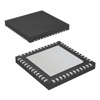
48-pin VQFN (RGZ) Package
Industrial Temperature Range: –40°C to +85°C
2 Applications
•
•
•
Distribution for High-Speed SERDES
Distribution of SERDES Reference Clocks for
1G/10G Ethernet, 1X/2X/4X/10X Fibre Channel,
PCI Express, Serial ATA, SONET, CPRI, OBSAI,
etc.
Up to 1-to-10 Clock Buffering and Fan-out
The CDCL1810 supports one differential LVDS clock
input and a total of 10 differential CML outputs. The
CML outputs are compatible with LVDS receivers if
they are ac-coupled.
With careful observation of the input voltage swing
and common-mode voltage limits, the CDCL1810 can
support a single-ended clock input as outlined in Pin
Configuration and Functions.
All device settings are programmable through the
SDA/SCL, serial two-wire interface. The serial
interface is 1.8V tolerant only.
The phase of one output group relative to the other
can be adjusted through the SDA/SCL interface. For
post-divide ratios (P0, P1) that are multiples of 5, the
total number of phase adjustment steps (n) equals
the divide-ratio divided by 5. For post-divide ratios
(P0, P1) that are not multiples of 5, the total number
of steps (n) is the same as the post-divide ratio. The
phase adjustment step (ΔΦ) in time units is given as:
ΔΦ = 1/(n × FOUT), where FOUT is the respective
output frequency.
The device operates in a 1.8-V supply environment
and is characterized for operation from –40°C to
+85°C. The CDCL1810 is available in a 48-pin VQFN
(RGZ) package.
Device Information(1)
PART NUMBER
CDCL1810
PACKAGE
VQFN (48)
BODY SIZE (NOM)
7.00 mm × 7.00 mm
(1) For all available packages, see the orderable addendum at
the end of the datasheet.
4 Functional Block Diagram
DIVIDER
5 Differential
CML Outputs
Up to 650MHz
DIVIDER
5 Differential
CML Outputs
Up to 650MHz
Differential
LVDS Input
Up to 650MHz
SDA/SCL
1
An IMPORTANT NOTICE at the end of this data sheet addresses availability, warranty, changes, use in safety-critical applications,
intellectual property matters and other important disclaimers. PRODUCTION DATA.
�CDCL1810
SLLS781D – FEBRUARY 2007 – REVISED NOVEMBER 2014
www.ti.com
Table of Contents
1
2
3
4
5
6
7
8
Features ..................................................................
Applications ...........................................................
Description .............................................................
Functional Block Diagram ....................................
Revision History.....................................................
Device Comparison Table.....................................
Pin Configuration and Functions .........................
Specifications.........................................................
1
1
1
1
2
3
4
6
8.1
8.2
8.3
8.4
8.5
8.6
8.7
6
6
6
6
6
7
Absolute Maximum Ratings .....................................
Handling Ratings.......................................................
Recommended Operating Conditions.......................
Thermal Information ..................................................
DC Electrical Characteristics ...................................
AC Electrical Characteristics.....................................
AC Electrical Characteristics for The SDA/SCL
Interface ....................................................................
8.8 Typical Characteristics ..............................................
9
8
9
Detailed Description ............................................ 10
9.1
9.2
9.3
9.4
9.5
9.6
9.7
Overview ................................................................. 10
Functional Block Diagrams ..................................... 10
Feature Description................................................. 11
SDA/SCL Connections Recommendations............. 12
Device Functional Modes........................................ 12
Programming........................................................... 13
SDA/SCL Bus Configuration Command Bitmap ..... 15
10 Application and Implementation........................ 21
10.1 Application Information.......................................... 21
11 Power Supply Recommendations ..................... 22
12 Layout................................................................... 22
12.1 Layout Guidelines ................................................. 22
12.2 Layout Example .................................................... 23
13 Device and Documentation Support ................. 25
13.1 Trademarks ........................................................... 25
13.2 Electrostatic Discharge Caution ............................ 25
13.3 Glossary ................................................................ 25
14 Mechanical, Packaging, and Orderable
Information ........................................................... 25
5 Revision History
Changes from Revision C (September 2014) to Revision D
Page
•
Changed the following values in AC Electrical Characteristics for Additive clock output jitter (JOUT): 188 to 180, 480
to 348, 514 to 338, 257 to 175, 500 to 347, 570 to 388, 27 to 41, 66 to 36, 72 to 42, 12 to 48, 23 to 33, 27 to 39, 3
to 0.7 ...................................................................................................................................................................................... 7
•
Updated Figure 8 ................................................................................................................................................................. 21
•
Added Detailed Design Procedure text ............................................................................................................................... 21
•
Updated images for Figure 9 and Figure 10 ........................................................................................................................ 22
Changes from Revision B (March 2011) to Revision C
Page
•
Added, updated, or renamed the following sections: Device Information Table, Application and Implementation;
Power Supply Recommendations; Layout; Device and Documentation Support; Mechanical, Packaging, and
Ordering Information .............................................................................................................................................................. 1
•
Added "and Automatic Output Synchronization" in Features ................................................................................................. 1
•
Deleted "Clock Synthesis" and "Synthesis" from Applications ............................................................................................... 1
•
Added Output Enable/Disable to Feature Description section ............................................................................................. 11
•
Added Figure 5 to Feature Description ................................................................................................................................ 11
Changes from Revision A (March 2007) to Revision B
Page
•
Changed the Decscription paragraph starting with "All device....interface"............................................................................ 1
•
Added Thermal Information table ........................................................................................................................................... 2
•
Changed The Description of row SCL in the Pin Function table: added "SCL tolerated 1.8V on the input only." ................ 5
•
Changed The Description of row SDA in the Pin Function table: added "SCD tolerates 1.8V on the input only." ............... 5
•
Changed -0.3 to 4.0 to -0.3 to VDD+0.6 in ABS MAX table................................................................................................... 6
•
Added Thermal Information table ........................................................................................................................................... 6
•
Changed the VD,DOUT Test Conditions in the AC Electrical Characteristics table ................................................................... 7
2
Submit Documentation Feedback
Copyright © 2007–2014, Texas Instruments Incorporated
Product Folder Links: CDCL1810
�CDCL1810
www.ti.com
SLLS781D – FEBRUARY 2007 – REVISED NOVEMBER 2014
•
Added Note 1 to the Function Block Diagram ...................................................................................................................... 10
•
Added the SDA/SCL Connections Recommendations section ............................................................................................ 12
6 Device Comparison Table
Table 1. TA Device Comparison
TA
PACKAGED DEVICES
–40°C to +85°C
CDCL1810RGZT
48-pin VQFN (RGZ) Package, small tape and reel
FEATURES
–40°C to +85°C
CDCL1810RGZR
48-pin VQFN (RGZ) Package, tape and reel
Table 2. Device Feature Comparison
FEATURE
CDCL1810
CDCL1810A
Divider Synchronization after power up and after each programming
access. During Synchronization all outputs Yes No are disabled.
Yes
No
Output Group Phase Adjustment
Yes
No
Device Revision ID
b'011'
b'100'
1:10 Clock Fanout
Yes
Yes
Outputs grouped into two divider banks
Yes
Yes
Individual Output enabled/disable with I2C
Yes
Yes
Continuous and independent operation of outputs which are not
programmed, while configuring and programming No Yes other
outputs.
No
Yes
Submit Documentation Feedback
Copyright © 2007–2014, Texas Instruments Incorporated
Product Folder Links: CDCL1810
3
�CDCL1810
SLLS781D – FEBRUARY 2007 – REVISED NOVEMBER 2014
www.ti.com
7 Pin Configuration and Functions
NC
AVDD
NC
NC
AVDD
YP9
YN9
VDD
YP8
YN8
VDD
ADD1
48
47
46
45
44
43
42
41
40
39
38
37
48-PIN VQFN
Package RGZ
(Top View)
NC
1
36
ADD0
AVDD
2
35
VDD
CLKP
3
34
YN7
CLKN
4
33
YP7
AVDD
5
32
VDD
YP0
6
31
YN6
CDCL1810
24
SDA
SCL
25
23
12
VDD
VSS
22
VDD
YN4
26
21
11
YP4
VDD
20
YP5
VDD
27
19
10
YN3
YN1
18
YN5
YP3
28
17
9
VDD
YP1
16
VDD
YN2
29
15
8
YP2
VDD
14
YP6
VDD
30
13
7
NC
YN0
NOTE: Exposed thermal pad must be soldered to VSS.
The CDCL1810 is available in a 48-pin VQFN (RGZ) package with a pin pitch of 0.5 mm. The exposed thermal pad
serves both thermal and electrical grounding purposes.
The device must be soldered to ground (VSS) using as many ground vias as possible. The device performance
will be severely impacted if the exposed thermal pad is not grounded appropriately.
4
Submit Documentation Feedback
Copyright © 2007–2014, Texas Instruments Incorporated
Product Folder Links: CDCL1810
�CDCL1810
www.ti.com
SLLS781D – FEBRUARY 2007 – REVISED NOVEMBER 2014
Pin Functions
PIN
NAME
PIN NO.
TYPE
DESCRIPTION
8, 11, 14, 17,
20, 23, 26,
29, 32, 35,
38, 41
Power
1.8-V digital power supply.
AVDD
2, 5, 44, 47
Power
1.8-V analog power supply.
VSS
Exposed
thermal pad
and pin 12
Power
Ground reference.
NC
1, 13, 45, 46,
48
I
Not connected; leave open.
3, 4
I
Differential LVDS input. Single-ended 1.8-V input can be dc-coupled to pin 3 with pin 4 either tied
to pin 3 (recommended) or left open.
6, 7
9, 10
15, 16
18, 19
21, 22
27, 28
30, 31
33, 34
40, 39
43, 42
O
10 differential CML outputs.
SCL
24
I
SCL serial clock pin. SCL tolerated 1.8V on the input only. Open drain. Always connect to a pullup resistor.
SDA
25
I/O
37, 36
I
VDD
CLKP, CLKN
YP0, YN0
YP1, YN1
YP2, YN2
YP3, YN3
YP4, YN4
YP5, YN5
YP6, YN6
YP7, YN7
YP8, YN8
YP9, YN9
ADD1, ADD0
SDA bidirectional serial data pin. SDA tolerates 1.8 V on the input only.Open drain. Always
connect to a pull-up resistor.
Configurable least significant bits (ADD[1:0]) of the SDA/SCL device address. The fixed most
significant bits (ADD[6:2]) of the 7-bit device address are 11010.
Submit Documentation Feedback
Copyright © 2007–2014, Texas Instruments Incorporated
Product Folder Links: CDCL1810
5
�CDCL1810
SLLS781D – FEBRUARY 2007 – REVISED NOVEMBER 2014
www.ti.com
8 Specifications
8.1 Absolute Maximum Ratings (1)
Over operating free-air temperature range (unless otherwise noted).
VDD, AVDD
Supply voltage (2)
(2)
VLVDS
Voltage range at LVDS input pins
VI
Voltage range at all non-LVDS input pins (2)
(1)
(2)
MIN
MAX
UNIT
–0.3
2.5
V
–0.3
VDD+0.6
V
–0.3
VDD+0.6
V
Stresses beyond those listed under absolute maximum ratings may cause permanent damage to the device. These are stress ratings
only, and functional operation of the device at these or any other conditions beyond those indicated under recommended operating
condition is not implied. Exposure to absolute-maximum-rated conditions for extended periods may affect device reliability.
All voltage values are with respect to network ground terminal.
8.2 Handling Ratings
Tstg
V(ESD)
(1)
(2)
MIN
MAX
UNIT
–65
+150
°C
Storage temperature range
Electrostatic discharge
Human body model (HBM), per ANSI/ESDA/JEDEC JS-001, all
pins (1)
2000
Charged device model (CDM), per JEDEC specification
JESD22-C101, all pins (2)
1500
V
JEDEC document JEP155 states that 2000-V HBM allows safe manufacturing with a standard ESD control process.
JEDEC document JEP157 states that 1500-V CDM allows safe manufacturing with a standard ESD control process.
8.3 Recommended Operating Conditions
Over operating free-air temperature range (unless otherwise noted).
MIN
NOM
MAX
UNIT
VDD
Digital supply voltage
1.7
1.8
1.9
V
AVD
Analog supply voltage
1.7
1.8
1.9
V
TA
Ambient temperature (no airflow, no heatsink)
–40
+85
°C
TJ
Junction temperature
+105
°C
D
8.4 Thermal Information
CDCL1810
THERMAL METRIC (1)
RGZ Package
UNIT
48 PINS
28.3, Airflow = 0 LFM
RθJA
Junction-to-ambient thermal resistance (2)
RθJC(top)
Junction-to-case (top) thermal resistance
20.5
RθJC(bot)
Junction-to-case (bottom) thermal resistance
5.3
(1)
(2)
22.4, Airflow = 50 LFM
°C/W
For more information about traditional and new thermal metrics, see the IC Package Thermal Metrics application report, SPRA953.
No heatsink; power uniformly distributed; 36 ground vias (6 x 6 array) tied to the thermal exposed pad; 4-layer high-K board.
8.5
DC Electrical Characteristics
Over recommended operating conditions (unless otherwise noted).
TEST CONDITIONS
MIN
TYP
MAX
UNIT
IVDD
Total current from digital 1.8-V supply
All outputs enabled; VDD = VDD,typ
650MHz LVDS input
IAVDD
Total current from analog 1.8-V supply
All outputs enabled; AVDD = VDD,typ
650MHz LVDS input
VIL,CMOS
Low level CMOS input voltage
VDD = 1.8 V
–0.2
0.6
V
VIH,CMOS
High level CMOS input voltage
VDD = 1.8 V
VDD –0.6
VDD
V
6
Submit Documentation Feedback
212
mA
16
mA
Copyright © 2007–2014, Texas Instruments Incorporated
Product Folder Links: CDCL1810
�CDCL1810
www.ti.com
SLLS781D – FEBRUARY 2007 – REVISED NOVEMBER 2014
DC Electrical Characteristics (continued)
Over recommended operating conditions (unless otherwise noted).
TEST CONDITIONS
MIN
TYP
MAX
UNIT
IIL,CMOS
Low level CMOS input current
VDD = VDD,max, VIL = 0.0 V
–120
μA
IIH,CMOS
High level CMOS input current
VDD = VDD,max, VIH = 1.9 V
65
μA
VOL,SDA
Low level CMOS output voltage for the
SDA pin
Sink current = 3 mA
0.2VDD
V
IOL,CMOS
Low level CMOS output current
0
8
mA
8.6 AC Electrical Characteristics
Over recommended operating conditions (unless otherwise noted).
TEST CONDITIONS
MIN
TYP
MAX
132
Ω
1200
1375
mV
ZD,IN
Differential input impedance for the LVDS input terminals
VCM,IN
Common-mode voltage, LVDS input
VS,IN
Single-ended LVDS input voltage swing
100
600
mVPP
VD,IN
Differential LVDS input voltage swing
200
1200
mVPP
tR,OUT,
tF,OUT
Output signal rise/fall time
VCM,OUT
Common-mode voltage, CML outputs
VS,OUT
Single-ended CML output voltage swing
VD,OUT
Differential CML output voltage swing
FIN
Clock input frequency
FOUT
Clock output frequency
1125
20%–80%
VDD –
0.31
VDD –
0.23
VDD –
0.19
ac-coupled
180
230
280
mVPP
measured in a 50-Ω
scope; The CML output
incorporates 50-Ω
resistors to VDD
360
460
560
mVPP
650
MHz
V
650
MHz
fs RMS
1MHz–5MHz offset
348
fs RMS
12kHz–5MHz offset
388
fs RMS
10Hz–1MHz offset
175
fs RMS
1MHz–5MHz offset
347
fs RMS
12kHz–5MHz offset
388
fs RMS
10Hz–1MHz offset
41
fs RMS
1MHz–20MHz offset
36
fs RMS
12kHz–20MHz offset
42
fs RMS
10Hz–1MHz offset
48
fs RMS
1MHz–20MHz offset
33
fs RMS
12kHz–20MHz offset
39
fs RMS
Input-to-output delay
FIN = 30.72MHz,
FOUT = 30.72MHz
YP[9:0] outputs
0.7
ns
Clock output skew
FIN = 30.72MHz,
FOUT = 30.72MHz
YP[9:0] outputs relative
to YP[0]
Additive clock output jitter
FIN = 650MHz, FOUT =
650MHz
VD,IN = 200mVPP
FIN = 650MHz, FOUT =
650MHz
VD,IN = 1200mVPP
TSOUT
ps
180
FIN = 30.72MHz, FOUT =
30.72MHz
VD,IN = 1200mVPP
TP
100
10Hz–1MHz offset
FIN = 30.72MHz, FOUT =
30.72MHz
VD,IN = 200mVPP
JOUT
90
UNIT
–64
64
Submit Documentation Feedback
Copyright © 2007–2014, Texas Instruments Incorporated
Product Folder Links: CDCL1810
ps
7
�CDCL1810
SLLS781D – FEBRUARY 2007 – REVISED NOVEMBER 2014
www.ti.com
AC Electrical Characteristics for The SDA/SCL Interface (1)
8.7
PARAMETER
MIN
TYP
MAX
UNIT
400
kHz
fSCL
SCL frequency
th(START)
START hold time
0.6
μs
tw(SCLL)
SCL low-pulse duration
1.3
μs
tw(SCLH)
SCL high-pulse duration
0.6
μs
tsu(START)
START setup time
0.6
μs
th(SDATA)
SDA hold time
0
μs
tsu(DATA)
SDA setup time
tr(SDATA)
SCL / SDA input rise time
0.3
μs
tf(SDATA)
SCL / SDA input fall time
0.3
μs
tsu(STOP)
STOP setup time
0.6
μs
tBUS
bus free time
1.3
μs
(1)
μs
0.6
See Figure 1 for the timing behavior.
S
P
tw(SCLL)
Bit 7 (MSB)
tw(SCLH)
Bit 6
tr(SM)
Bit 0 (LSB)
A
P
tf(SM)
VIH(SM)
SCL
VIL(SM)
tSU(START)
t(BUS)
th(START)
tSU(SDATA)
tr(SM)
th(SDATA)
tSU(STOP)
tf(SM)
VIH(SM)
SDA
VIL(SM)
Figure 1. Timing Diagram for the SDA/SCL Serial Control Interface
8
Submit Documentation Feedback
Copyright © 2007–2014, Texas Instruments Incorporated
Product Folder Links: CDCL1810
�CDCL1810
www.ti.com
SLLS781D – FEBRUARY 2007 – REVISED NOVEMBER 2014
8.8 Typical Characteristics
Typical operating conditions are at VDD = 1.8V and TA = +25°C, VD,IN = 200mVPP (unless otherwise noted).
300
Differential Output Voltage - mV
Differential Output Voltage - mV
300
200
100
0
-100
-200
-300
0
20
40
60
t - Time - ns
80
100
200
100
0
-100
-200
-300
0
Figure 2. Transient Performance:
FIN = 30.72 MHz, FOUT = 30.72 MHz
1
2
3
t - Time - ns
4
Figure 3. Transient Performance:
FIN = 650 MHz, FOUT = 650 MHz
Submit Documentation Feedback
Copyright © 2007–2014, Texas Instruments Incorporated
Product Folder Links: CDCL1810
5
9
�CDCL1810
SLLS781D – FEBRUARY 2007 – REVISED NOVEMBER 2014
www.ti.com
9 Detailed Description
9.1 Overview
The CDCL1810 is a high-performance 10 output clock distributor. The device operates form a single 1.8-V
supply. The outputs are grouped in to banks of 5 outputs each with independent frequency division ratios.
9.2 Functional Block Diagrams
DIVIDER
5 Differential
CML Outputs
Up to 650MHz
DIVIDER
5 Differential
CML Outputs
Up to 650MHz
Differential
LVDS Input
Up to 650MHz
SDA/SCL
Figure 4. SDA/SCL Interface
VDD
Divider
P1
YP[9:5]
CML
CML
YN[9:5]
CLKP
LVDS
CLKN
Divider
P0
YP[4:0]
CML
CML
YN[4:0]
Divider Setting
SDA/SCL
SDA/SCL
Control
See Note 1
VSS
Note 1: Outputs can be disabled to floating. When outputs are left floating, internal 50 Ω termination to VDD pulls both
YN and YP to VDD.
10
Submit Documentation Feedback
Copyright © 2007–2014, Texas Instruments Incorporated
Product Folder Links: CDCL1810
�CDCL1810
www.ti.com
SLLS781D – FEBRUARY 2007 – REVISED NOVEMBER 2014
9.3 Feature Description
9.3.1 Output Enable/Disable
The CDCL1810 does not require external output synchronization. Instead the device incorporates a scheme
which ensures the output dividers are reset and time synchronized after every write action into the I2C
programmable register space.
power up
POR verifies input supply
Load register defaults
Reload all divider settings;
Reset all dividers
Enable all selected output
banks
Device active
(normal mode)
no
I2C register write
command?
yes
Disable all outputs
Figure 5. Device Status Flow Chart
Submit Documentation Feedback
Copyright © 2007–2014, Texas Instruments Incorporated
Product Folder Links: CDCL1810
11
�CDCL1810
SLLS781D – FEBRUARY 2007 – REVISED NOVEMBER 2014
www.ti.com
9.4 SDA/SCL Connections Recommendations
The serial interface inputs don’t have glitch suppression circuit. So, any noises or glitches at serial input lines
may cause programming error. The serial interface lines should be routed in such a way that the lines would
have minimum noise impact from the surroundings.
Figure 6 is recommended to improve the interconnections.
RP
SCL
CF
Master
CDCL1810
(Slave)
RP
SDA
Figure 6. Serial Interface Connections
Lower RP resistor value (around 1 kΩ) should be chosen so that signals will have faster rise time. A capacitor
can be connected to SCL line to ground which will act as a filter.
An I2C level translator will help to overcome the noises issue.
9.5 Device Functional Modes
The device is designed to operate from an input voltage supply of 1.8 V. In the default power on reset, all device
outputs are enabled and the dividers P0 and P1 are set to 1.
12
Submit Documentation Feedback
Copyright © 2007–2014, Texas Instruments Incorporated
Product Folder Links: CDCL1810
�CDCL1810
www.ti.com
SLLS781D – FEBRUARY 2007 – REVISED NOVEMBER 2014
9.6 Programming
9.6.1 SDA/SCL Interface
This section describes the SDA/SCL interface of the CDCL1810 device. The CDCL1810 operates as a slave
device of the industry standard 2-pin SDA/SCL bus. It operates in the fast-mode at a bit-rate of up to 400 kbit/s
and supports 7-bit addressing compatible with the popular 2-pin serial interface standard.
9.6.1.1 SDA/SCL Bus Slave Device Address
A6
A5
A4
A3
A2
A1
A0
R/W
1
1
0
1
0
ADD1
ADD0
0/1
The device address is made up of the fixed internal address, 11010 (A6:A2), and configurable external pins
ADD1 (A1) and ADD0 (A0). Four different devices with addresses 1101000, 1101001, 1101010 and 1101011,
can be addressed via the same SDA/SCL bus interface. The least significant bit of the address byte designates a
write or read operation.
R/W Bit:
0 = write to CDCL1810 device
1 = read from CDCL1810 device
9.6.1.2 Command Code Definition
BIT
DESCRIPTION
C7
1 = Byte Write / Read or Word Write / Read operation
(C6:C0)
Byte Offset for Byte Write / Read and Word Write / Read operation.
COMMAND CODE for Byte Write / Read
OPERATION
HEX
CODE
C7
C6
C5
C4
C3
C2
C1
C0
byte 0
80h
1
0
0
0
0
0
0
0
byte 1
81h
1
0
0
0
0
0
0
1
byte 2
82h
1
0
0
0
0
0
1
0
byte 3
83h
1
0
0
0
0
0
1
1
byte 4
84h
1
0
0
0
0
1
0
0
byte 5
85h
1
0
0
0
0
1
0
1
byte 6
86h
1
0
0
0
0
1
1
0
HEX
CODE
C7
C6
C5
C4
C3
C2
C1
C0
word 0: byte 0 and byte 1
80h
1
0
0
0
0
0
0
0
word 1: byte 1 and byte 2
81h
1
0
0
0
0
0
0
1
word 2: byte 2 and byte 3
82h
1
0
0
0
0
0
1
0
word 3: byte 3 and byte 4
83h
1
0
0
0
0
0
1
1
word 4: byte 4 and byte 5
84h
1
0
0
0
0
1
0
0
word 5: byte 5 and byte 6
85h
1
0
0
0
0
1
0
1
word 6: byte 6 and byte 7
86h
1
0
0
0
0
1
1
0
COMMAND CODE for Word Write / Read
OPERATION
Submit Documentation Feedback
Copyright © 2007–2014, Texas Instruments Incorporated
Product Folder Links: CDCL1810
13
�CDCL1810
SLLS781D – FEBRUARY 2007 – REVISED NOVEMBER 2014
www.ti.com
9.6.1.3 SDA/SCL Programming Sequence
1
7
S
Slave Address
1
1
Wr A
S
Start condition
Sr
Repeated start condition
Rd
Read (bit value = 1)
Wr
Write (bit value = 0)
A
Acknowledge (bit value = 0)
N
Not acknowledge (bit value = 1)
P
Stop condition
8
Data Byte
1
1
A
P
Master to Slave transmission
Slave to Master transmission
Figure 7. Legend for Programming Sequence
Byte Write Programming Sequence:
1
7
1
1
8
1
8
1
1
S
Slave Address
Wr
A
Command Code
A
Data Byte
A
P
Byte Read Programming Sequence:
1
S
7
1
Wr
Slave Address
1
8
1
1
7
1
1
8
1
1
A
Command
Code
A
S
Slave Address
Rd
A
Data Byte
N
P
Word Write Programming Sequence:
1
7
1
1
8
1
8
1
8
1
1
S
Slave Address
Wr
A
Command Code
A
Data Byte Low
A
Data Byte High
A
P
Word Read Programming Sequence:
14
1
7
S
Slave
Address
1
Wr
1
8
A
Command
Code
1
A
1
7
1
1
8
1
8
1
1
S
Slave
Address
Rd
A
Data Byte
A
Data Byte
N
P
Submit Documentation Feedback
Copyright © 2007–2014, Texas Instruments Incorporated
Product Folder Links: CDCL1810
�CDCL1810
www.ti.com
SLLS781D – FEBRUARY 2007 – REVISED NOVEMBER 2014
9.7 SDA/SCL Bus Configuration Command Bitmap
9.7.1 Byte 0:
BIT
BIT NAME
DESCRIPTION/FUNCTION
POWER UP
CONDITION
REFERENCE
TO
TYPE
POWER UP
CONDITION
REFERENCE
TO
TYPE
7
MANF[7]
Manufacturer reserved
R
6
MANF[6]
Manufacturer reserved
R
5
MANF[5]
Manufacturer reserved
R
4
MANF[4]
Manufacturer reserved
R
3
MANF[3]
Manufacturer reserved
R
2
MANF[2]
Manufacturer reserved
R
1
MANF[1]
Manufacturer reserved
R
0
MANF[0]
Manufacturer reserved
R
9.7.2 Byte 1:
BIT
BIT NAME
DESCRIPTION/FUNCTION
7
RES
Reserved
R/W
0
6
RES
Reserved
R/W
0
5
ENPH
Phase select enable
R/W
1
4
PH1[4]
Phase select for YP[9:5] and YN[9:5]
R/W
0
Table 4, Table 5
3
PH1[3]
Phase select for YP[9:5] and YN[9:5]
R/W
0
Table 4, Table 5
2
PH1[2]
Phase select for YP[9:5] and YN[9:5]
R/W
0
Table 4, Table 5
1
PH1[1]
Phase select for YP[9:5] and YN[9:5]
R/W
0
Table 4, Table 5
0
PH1[0]
Phase select for YP[9:5] and YN[9:5]
R/W
0
Table 4, Table 5
TYPE
POWER UP
CONDITION
REFERENCE
TO
9.7.3 Byte 2:
BIT
BIT NAME
DESCRIPTION/FUNCTION
7
RES
Reserved
R/W
0
6
RES
Reserved
R/W
0
5
ENP1
Post-divider P1 enable; if 0 output YP[9:5] and YN[9:5] are disabled
R/W
1
4
RES
Reserved
R/W
1
3
SELP1[3]
Divide ratio select for post-divider P1
R/W
0
Table 3
2
SELP1[2]
Divide ratio select for post-divider P1
R/W
0
Table 3
1
SELP1[1]
Divide ratio select for post-divider P1
R/W
0
Table 3
0
SELP1[0]
Divide ratio select for post-divider P1
R/W
0
Table 3
Submit Documentation Feedback
Copyright © 2007–2014, Texas Instruments Incorporated
Product Folder Links: CDCL1810
15
�CDCL1810
SLLS781D – FEBRUARY 2007 – REVISED NOVEMBER 2014
www.ti.com
9.7.4 Byte 3:
BIT
BIT NAME
DESCRIPTION/FUNCTION
TYPE
POWER UP
CONDITION
REFERENCE
TO
7
RES
Reserved
R/W
0
6
RES
Reserved
R/W
0
5
RES
Reserved
R/W
0
4
PH0[4]
Phase select for YP[4:0] and YN[4:0]
R/W
0
Table 4, Table 5
3
PH0[3]
Phase select for YP[4:0] and YN[4:0]
R/W
0
Table 4, Table 5
2
PH0[2]
Phase select for YP[4:0] and YN[4:0]
R/W
0
Table 4, Table 5
1
PH0[1]
Phase select for YP[4:0] and YN[4:0]
R/W
0
Table 4, Table 5
0
PH0[0]
Phase select for YP[4:0] and YN[4:0]
R/W
0
Table 4, Table 5
TYPE
POWER UP
CONDITION
REFERENCE
TO
9.7.5 Byte 4:
BIT
BIT NAME
DESCRIPTION/FUNCTION
7
RES
Reserved
R/W
0
6
RES
Reserved
R/W
0
5
ENP0
Post-divider P0 enable. If 0, output YP[4:0] and YN[4:0] are disabled
R/W
1
4
RES
Reserved
R/W
1
3
SELP0[3]
Divide ratio select for post-divider P0
R/W
0
Table 3
2
SELP0[2]
Divide ratio select for post-divider P0
R/W
0
Table 3
1
SELP0[1]
Divide ratio select for post-divider P0
R/W
0
Table 3
0
SELP0[0]
Divide ratio select for post-divider P0
R/W
0
Table 3
TYPE
POWER UP
CONDITION
REFERENCE
TO
R/W
1
R
1
9.7.6 Byte 5:
BIT
16
BIT NAME
DESCRIPTION/FUNCTION
7
EN
Chip enable; if 0 chip is in Iddq mode
6
RES
Reserved
5
ENDRV9
YP[9], YN[9] enable; if 0 output is disabled
R/W
1
4
ENDRV8
YP[8], YN[8] enable; if 0 output is disabled
R/W
1
3
ENDRV7
YP[7], YN[7] enable; if 0 output is disabled
R/W
1
2
ENDRV6
YP[6], YN[6] enable; if 0 output is disabled
R/W
1
1
ENDRV5
YP[5], YN[5] enable; if 0 output is disabled
R/W
1
0
ENDRV4
YP[4], YN[4] enable; if 0 output is disabled
R/W
1
Submit Documentation Feedback
Copyright © 2007–2014, Texas Instruments Incorporated
Product Folder Links: CDCL1810
�CDCL1810
www.ti.com
SLLS781D – FEBRUARY 2007 – REVISED NOVEMBER 2014
9.7.7 Byte 6:
BIT
BIT NAME
DESCRIPTION/FUNCTION
TYPE
POWER UP
CONDITION
7
ENDRV3
YP[3], YN[3] enable; if 0 output is disabled
R/W
1
6
ENDRV2
YP[2], YN[2] enable; if 0 output is disabled
R/W
1
5
ENDRV1
YP[1], YN[1] enable; if 0 output is disabled
R/W
1
4
ENDRV0
YP[0], YN[0] enable; if 0 output is disabled
R/W
1
3
RES
Reserved
R/W
0
2
RES
Reserved
R/W
0
1
RES
Reserved
R/W
0
0
RES
Reserved
R/W
0
REFERENCE
TO
Table 3. Divide Ratio Settings for Post-Divider P0 or P1
DIVIDE
RATIO
SELP1[3] or
SELP0[3]
SELP1[2] or
SELP0[2]
SELP1[1] or
SELP0[1]
SELP1[0] or
SELP0[0]
NOTES
1
0
0
0
0
Default
2
0
0
0
1
4
0
0
1
0
5
0
0
1
1
8
0
1
0
0
10
0
1
0
1
16
0
1
1
0
20
0
1
1
1
32
1
0
0
0
40
1
0
0
1
80
1
0
1
0
Table 4. Phase Settings for Divide Ratio = 5, 10, 20, 40, 80
WITH PH0[4:0] = 00000
DIVIDE
RATIO
PHASE LEAD
(RADIAN)
PH1
[4]
[3]
[2]
[1]
[0]
5
X
X
X
X
X
0
10
X
X
X
0
X
0
X
X
X
1
X
(2π/2)
X
X
0
0
X
0
X
X
0
1
X
(2π/4)
X
X
1
0
X
2(2π/4)
X
X
1
1
X
3(2π/4)
X
0
0
0
X
0
X
0
0
1
X
(2π/8)
X
0
1
0
X
2(2π/8)
X
0
1
1
X
3(2π/8)
X
1
0
0
X
4(2π/8)
X
1
0
1
X
5(2π/8)
X
1
1
0
X
6(2π/8)
X
1
1
1
X
7(2π/8)
20
40
NOTES
Phase setting not available
Submit Documentation Feedback
Copyright © 2007–2014, Texas Instruments Incorporated
Product Folder Links: CDCL1810
17
�CDCL1810
SLLS781D – FEBRUARY 2007 – REVISED NOVEMBER 2014
www.ti.com
Table 4. Phase Settings for Divide Ratio = 5, 10, 20, 40, 80 (continued)
WITH PH0[4:0] = 00000
DIVIDE
RATIO
80
18
PHASE LEAD
(RADIAN)
PH1
[4]
[3]
[2]
[1]
[0]
0
0
0
0
X
0
0
0
0
1
X
(2π/16)
0
0
1
0
X
2(2π/16)
0
0
1
1
X
3(2π/16)
0
1
0
0
X
4(2π/16)
0
1
0
1
X
5(2π/16)
0
1
1
0
X
6(2π/16)
0
1
1
1
X
7(2π/16)
1
0
0
0
X
8(2π/16)
1
0
0
1
X
9(2π/16)
1
0
1
0
X
10(2π/16)
1
0
1
1
X
11(2π/16)
1
1
0
0
X
12(2π/16)
1
1
0
1
X
13(2π/16)
1
1
1
0
X
14(2π/16)
1
1
1
1
X
15(2π/16)
Submit Documentation Feedback
NOTES
Copyright © 2007–2014, Texas Instruments Incorporated
Product Folder Links: CDCL1810
�CDCL1810
www.ti.com
SLLS781D – FEBRUARY 2007 – REVISED NOVEMBER 2014
Table 5. Phase Settings for Divide Ratio = 1, 2, 4, 8, 16, 32
WITH PH0[4:0] = 00000
DIVIDE
RATIO
PHASE LEAD
(RADIAN)
PH1
[4]
[3]
[2]
[1]
[0]
1
X
X
X
X
X
0
2
X
X
X
X
0
0
X
X
X
X
1
(2π/2)
X
X
X
0
0
0
X
X
X
0
1
(2π/4)
X
X
X
1
0
2(2π/4)
X
X
X
1
1
3(2π/4)
X
X
0
0
0
0
X
X
0
0
1
(2π/8)
X
X
0
1
0
2(2π/8)
X
X
0
1
1
3(2π/8)
X
X
1
0
0
4(2π/8)
X
X
1
0
1
5(2π/8)
X
X
1
1
0
6(2π/8)
X
X
1
1
1
7(2π/8)
X
0
0
0
0
0
X
0
0
0
1
(2π/16)
X
0
0
1
0
2(2π/16)
X
0
0
1
1
3(2π/16)
X
0
1
0
0
4(2π/16)
X
0
1
0
1
5(2π/16)
X
0
1
1
0
6(2π/16)
X
0
1
1
1
7(2π/16)
X
1
0
0
0
8(2π/16)
X
1
0
0
1
9(2π/16)
X
1
0
1
0
10(2π/16)
X
1
0
1
1
11(2π/16)
X
1
1
0
0
12(2π/16)
X
1
1
0
1
13(2π/16)
X
1
1
1
0
14(2π/16)
X
1
1
1
1
15(2π/16)
4
8
16
NOTES
00000: Default Phase setting not available
Submit Documentation Feedback
Copyright © 2007–2014, Texas Instruments Incorporated
Product Folder Links: CDCL1810
19
�CDCL1810
SLLS781D – FEBRUARY 2007 – REVISED NOVEMBER 2014
www.ti.com
Table 5. Phase Settings for Divide Ratio = 1, 2, 4, 8, 16, 32 (continued)
WITH PH0[4:0] = 00000
DIVIDE
RATIO
32
20
PHASE LEAD
(RADIAN)
PH1
[4]
[3]
[2]
[1]
[0]
0
0
0
0
0
0
0
0
0
0
1
(2π/32)
0
0
0
1
0
2(2π/32)
0
0
0
1
1
3(2π/32)
0
0
1
0
0
4(2π/32)
0
0
1
0
1
5(2π/32)
0
0
1
1
0
6(2π/32)
0
0
1
1
1
7(2π/32)
0
1
0
0
0
8(2π/32)
0
1
0
0
1
9(2π/32)
0
1
0
1
0
10(2π/32)
0
1
0
1
1
11(2π/32)
0
1
1
0
0
12(2π/32)
0
1
1
0
1
13(2π/32)
0
1
1
1
0
14(2π/32)
0
1
1
1
1
15(2π/32)
1
0
0
0
0
16(2π/32)
1
0
0
0
1
17(2π/32)
1
0
0
1
0
18(2π/32)
1
0
0
1
1
19(2π/32)
1
0
1
0
0
20(2π/32)
1
0
1
0
1
21(2π/32)
1
0
1
1
0
22(2π/32)
1
0
1
1
1
23(2π/32)
1
1
0
0
0
24(2π/32)
1
1
0
0
1
25(2π/32)
1
1
0
1
0
26(2π/32)
1
1
0
1
1
27(2π/32)
1
1
1
0
0
28(2π/32)
1
1
1
0
1
29(2π/32)
1
1
1
1
0
30(2π/32)
1
1
1
1
1
31(2π/32)
Submit Documentation Feedback
NOTES
Copyright © 2007–2014, Texas Instruments Incorporated
Product Folder Links: CDCL1810
�CDCL1810
www.ti.com
SLLS781D – FEBRUARY 2007 – REVISED NOVEMBER 2014
10 Application and Implementation
NOTE
Information in the following applications sections is not part of the TI component
specification, and TI does not warrant its accuracy or completeness. TI’s customers are
responsible for determining suitability of components for their purposes. Customers should
validate and test their design implementation to confirm system functionality.
10.1 Application Information
The CDCL1810 is a high-performance buffer that can generate 10 copies of CML clock outputs from a LVDS
input. The programmable dividers, P0 and P1, give a high flexibility to the ratio of the output frequency to the
input frequency.
10.1.1 Clock Distribution for Multiple TI Keystone DSPs
Figure 8. CDCL1810 Application Drawing
10.1.1.1 Design Requirements
A typical application example is multi DSP chip environment. The CDCL1810 is used to buffer the common
clocks to the DSP.
10.1.1.2 Detailed Design Procedure
The CDCL1810 supports output group phase alignment, if a divider gets reprogrammed. The output group phase
alignment circuit will disable all outputs after changing a single divider. The outputs are enabled after the phases
are aligned. See Figure 9.
If an output gets enabled/disabled, the phase synchronization circuit will ensure that all outputs are in phase. To
ensure phase alignment the outputs needs to be disabled for a short time. See Figure 10.
Submit Documentation Feedback
Copyright © 2007–2014, Texas Instruments Incorporated
Product Folder Links: CDCL1810
21
�CDCL1810
SLLS781D – FEBRUARY 2007 – REVISED NOVEMBER 2014
www.ti.com
Application Information (continued)
10.1.1.3 Application Curves
Y[4:0], div by 2
Y[9:5], div by 6
Figure 9. Output Group Divider Change
Y0
Y1
Enable
Figure 10. Individual Output Disable/Enable
11 Power Supply Recommendations
The device is designed to operate from an input voltage supply of 1.8 V for analog supply (AVDD) and core
supply (VDD). Both AVDD and VDD can be supplied by a single source.
12 Layout
12.1 Layout Guidelines
•
•
•
•
Keep the connections between the bypass capacitors and the power supply on the device as short as
possible.
Ground the other side of the capacitor using a low impedance connection to the ground plane.
If the capacitors are mounted on the back side, 0402 components can be employed; however, soldering to
the Thermal Dissipation Pad can be difficult.
For component side mounting, use 0201 body size capacitors to facilitate signal routing.
NOTE
The device must be soldered to ground (VSS) using as many ground vias as possible. The
device performance will be severely impacted if the exposed thermal pad is not grounded
appropriately.
22
Submit Documentation Feedback
Copyright © 2007–2014, Texas Instruments Incorporated
Product Folder Links: CDCL1810
�CDCL1810
www.ti.com
SLLS781D – FEBRUARY 2007 – REVISED NOVEMBER 2014
12.2 Layout Example
Figure 11. Layout Example: Signal Layer (TOP)
Submit Documentation Feedback
Copyright © 2007–2014, Texas Instruments Incorporated
Product Folder Links: CDCL1810
23
�CDCL1810
SLLS781D – FEBRUARY 2007 – REVISED NOVEMBER 2014
www.ti.com
Layout Example (continued)
Figure 12. Layout Example: Bottom Layer with Decoupling Capacitors
24
Submit Documentation Feedback
Copyright © 2007–2014, Texas Instruments Incorporated
Product Folder Links: CDCL1810
�CDCL1810
www.ti.com
SLLS781D – FEBRUARY 2007 – REVISED NOVEMBER 2014
13 Device and Documentation Support
13.1 Trademarks
All trademarks are the property of their respective owners.
13.2 Electrostatic Discharge Caution
These devices have limited built-in ESD protection. The leads should be shorted together or the device placed in conductive foam
during storage or handling to prevent electrostatic damage to the MOS gates.
13.3 Glossary
SLYZ022 — TI Glossary.
This glossary lists and explains terms, acronyms, and definitions.
14 Mechanical, Packaging, and Orderable Information
The following pages include mechanical, packaging, and orderable information. This information is the most
current data available for the designated devices. This data is subject to change without notice and revision of
this document. For browser-based versions of this data sheet, refer to the left-hand navigation.
Submit Documentation Feedback
Copyright © 2007–2014, Texas Instruments Incorporated
Product Folder Links: CDCL1810
25
�PACKAGE OPTION ADDENDUM
www.ti.com
14-Oct-2022
PACKAGING INFORMATION
Orderable Device
Status
(1)
Package Type Package Pins Package
Drawing
Qty
Eco Plan
(2)
Lead finish/
Ball material
MSL Peak Temp
Op Temp (°C)
Device Marking
(3)
Samples
(4/5)
(6)
CDCL1810RGZR
ACTIVE
VQFN
RGZ
48
2500
RoHS & Green
NIPDAU
Level-3-260C-168 HR
-40 to 85
CDCL
1810
Samples
CDCL1810RGZT
ACTIVE
VQFN
RGZ
48
250
RoHS & Green
NIPDAU
Level-3-260C-168 HR
-40 to 85
CDCL
1810
Samples
(1)
The marketing status values are defined as follows:
ACTIVE: Product device recommended for new designs.
LIFEBUY: TI has announced that the device will be discontinued, and a lifetime-buy period is in effect.
NRND: Not recommended for new designs. Device is in production to support existing customers, but TI does not recommend using this part in a new design.
PREVIEW: Device has been announced but is not in production. Samples may or may not be available.
OBSOLETE: TI has discontinued the production of the device.
(2)
RoHS: TI defines "RoHS" to mean semiconductor products that are compliant with the current EU RoHS requirements for all 10 RoHS substances, including the requirement that RoHS substance
do not exceed 0.1% by weight in homogeneous materials. Where designed to be soldered at high temperatures, "RoHS" products are suitable for use in specified lead-free processes. TI may
reference these types of products as "Pb-Free".
RoHS Exempt: TI defines "RoHS Exempt" to mean products that contain lead but are compliant with EU RoHS pursuant to a specific EU RoHS exemption.
Green: TI defines "Green" to mean the content of Chlorine (Cl) and Bromine (Br) based flame retardants meet JS709B low halogen requirements of