User's Guide
SCAU042 – July 2010
Low Additive Phase Noise LVCMOS Clock Buffer
Evaluation Board
NEED ABSTRACT
2
3
4
5
6
7
8
9
Contents
General Description .........................................................................................................
1.1
Features .............................................................................................................
Signal Path and Control Circuitry .........................................................................................
Getting Started ..............................................................................................................
Power-Supply Connections ................................................................................................
Enabling/Disabling the Outputs ...........................................................................................
Output Clock .................................................................................................................
Bill of Materials ..............................................................................................................
Schematic ....................................................................................................................
References ...................................................................................................................
1
Schematic (Page 1 of 3) ................................................................................................... 4
2
Schematic (Page 2 of 3) ................................................................................................... 5
3
Schematic (Page 31 of 3) .................................................................................................. 6
1
1
1
2
2
2
2
2
2
4
6
List of Figures
List of Tables
1
1
Bill of Materials .............................................................................................................. 2
General Description
The CDCLVC1112 is a high-performance, low additive phase noise LVCMOS clock buffer. It has one
LVCMOS input and twelve LVCMOS outputs. It has also an enable pin.
This evaluation module (EVM) is designed to demonstrate the electrical performance of the
CDCLVC1112.Throughout this document, the acronym EVM and the phrases evaluation module and
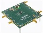
evaluation board are synonymous with the CDCLVC1112 EVM. Figure 1 illustrates the CDCLVC1112
EVM.
For optimum performance, the board is equipped with 50Ω SMA connectors and well controlled 50Ω
impedance microstrip transmission lines.
1.1
Features
•
•
•
•
Easy-to-use evaluation board to fan out low phase noise
Easy device setup
Enable pin configurable though jumper and SMA
Board powered at 3.3V
SCAU042 – July 2010
Low Additive Phase Noise LVCMOS Clock Buffer Evaluation Board
Copyright © 2010, Texas Instruments Incorporated
1
�Signal Path and Control Circuitry
2
www.ti.com
Signal Path and Control Circuitry
The CDCLVC1112 EVM supports single-ended inputs up to 250MHz. For more information about the
CDCLVC1112, see the CDCLVC1112 product data sheet available for download from the TI web site
(www.ti.com).
3
Getting Started
The CDCLVC1112EVM has self-explanatory labeling and uses similar naming conventions as the
CDCLVC1112 product datasheet. In this user’s guide, all words in boldface and italic print reflect the
actual labeling on the EVM.
4
Power-Supply Connections
Connect the power-supply source to the banana plug labeled VDD (P1), and connect the ground of the
power-supply source to GND (P2). There are decoupling capacitors and a ferrite bead to isolate the EVM
power from the CDCLVC1112 device power pins.
The CDCLVC1112EVM can use a supply voltage 3.0 to 3.6 V.
5
Enabling/Disabling the Outputs
The Enable pin of the CDCLVC1112 can be controlled using jumper J21 or the SMA J2. The J2 connector
is not soldered on the CDCLVC1112EVM but can be soldered if needed. Check the BOM section for part
ordering information.
6
Output Clock
The CDCLVC1112 generates twelve LVCMOS outputs. The outputs can be loaded using the pull-up and
pull-down footprints. No resistor has been soldered in those footprints.
7
Bill of Materials
Table 1. Bill of Materials
QTY
2
Value
Designator
PKG/Case
Manufacturer
Part Number
14
0
C1–C14
402
Panasonic – Ecg
ERJ-2GE0R00X
6
0.01µF
C19–C24
402
Venkel
C0402X7R500-103KNE
1
0.1µF
C18
402
Venkel
C0402X7R160-104KNE
2
47 µF
C15, C16
805
Taiyo Yuden
JMK212BJ476MG-T
1
10 µF
C17
3216-18 (EIA)
Kemet
B45196H3106K109
14
0.0 (Zero Ohm)
R4, R5, R8, R11, R14,
402
R17, R20, R23, R26,
R29, R32, R35, R38, R41
Panasonic – Ecg
ERJ-2GE0R00X
2
100
R1, R2
402
Venkel
CR0402-16W-1000FT
1
150
R43
402
Panasonic – Ecg
ERJ-2RKF1500X
1
50
L1
1206
Murata Electronics North Am
BLM31PG500SN1L
1
LED – Green
Clear
D1
1206
Cml Innovative Technologies
CMD15-21VGC/TR8
1
CDCLVC1112
U1
24-TSSOP
Texas Instruments
CDCLVC1112
1
1X3
J21
0.1 "
HTSW-150-07-G-S
K10000013783
2
Banana Plug –
Metal
P1, P2
4mm
Emerson Network Power Co
108-0740-001
5
142-0701-801
J1, J3, J7, J9, J11
RF SMA EDGE
Emerson Network Power Co
142-0701-801
4
4-40/0.25"
Screws
Building Fasteners
PMSSS 440 0025 PH
4
0.75"
Standoffs
2029
K10000010170
Round Threaded
Low Additive Phase Noise LVCMOS Clock Buffer Evaluation Board
Copyright © 2010, Texas Instruments Incorporated
SCAU042 – July 2010
�Bill of Materials
www.ti.com
Table 1. Bill of Materials (continued)
QTY
Value
Designator
26
DNI
R3, R6, R7, R9, R10,
402
R12, R13, R15, R16,
R18, R19, R21, R22,
R24, R25, R27, R28,
R30, R31, R33, R34,
R36, R37, R39, R40, R42
DNI
9
DNI
J2, J4–J6, J8, J10,
J12–J14
DNI
SCAU042 – July 2010
PKG/Case
Manufacturer
RF SMA EDGE
Part Number
Low Additive Phase Noise LVCMOS Clock Buffer Evaluation Board
Copyright © 2010, Texas Instruments Incorporated
3
�0
GND
P2
VDD
P1
4
2
1
1
1
1
J2
SMA
5
3
5
3
0
1
+
VDD_IN
0 Ohm
C2
1
R6
NU
R3
NU
0
L1
R2
100
C15
47uF
0
VDD
0 Ohm
2
C16
47uF
+
C17
10uF
FERRITE BEAD 50 ohm @ 100MHZ
0
R4
+
J21
0
C18
.1uF
1
2
3
VDD
2
1
C1
Y11
Y9
Y6
Y4
Y0
C19
.01uF
R5
0
2
1
1
C20
.01uF
0
VDD
2
1
4
2
C21
.01uF
2
1
R1
100
0
C22
.01uF
2
1
Copyright © 2010, Texas Instruments Incorporated
12
11
10
9
8
7
6
5
4
3
2
1
C23
.01uF
Y_10
VDD_5
C24
.01uF
CDCLVC1112
Y_12
GND_3
GND_5
Y_8
VDD_2
Y_9
Y_7
VDD_4
Y_5
GND_4
Y2
VDD_3
Y_3
Y_1
Y_6
GND_2
Y_4
VDD
GND
Y_0
Enable
CLK_IN
U1
2
Low Additive Phase Noise LVCMOS Clock Buffer Evaluation Board
1
J1
SMA
2
4
1
13
14
15
16
17
18
19
20
21
22
23
24
150
R43
VDD
D1
GREEN
Y10
Y8
Y7
Y5
Y2
Y3
Y1
8
1
2
VDD
Schematic
www.ti.com
Schematic
Figure 1. Schematic (Page 1 of 3)
SCAU042 – July 2010
�Copyright © 2010, Texas Instruments Incorporated
Y6
Y4
Y0
0
R14
0
R11
0
R8
0 Ohm
C5
0
0
VDD
0 Ohm
C4
0
VDD
0 Ohm
C3
1
J3
SMA
R15 J5
NU SMA
1
R13
Nu
R12 J4
NU SMA
1
R10
Nu
R9
NU
R7
Nu
5
3
5
3
5
3
4
2
4
2
4
2
0
0
0
Y10
Y11
Y9
0
R23
0
R20
0
R17
0 Ohm
C8
0
0
VDD
0 Ohm
C7
0
VDD
0 Ohm
C6
VDD
R24 J8
NU SMA
1
R22
Nu
R21 J7
NU SMA
1
R19
Nu
R18 J6
NU SMA
1
R16
Nu
5
3
5
3
SCAU042 – July 2010
5
3
VDD
4
2
4
2
4
2
0
0
0
www.ti.com
Schematic
Figure 2. Schematic (Page 2 of 3)
Low Additive Phase Noise LVCMOS Clock Buffer Evaluation Board
5
�Low Additive Phase Noise LVCMOS Clock Buffer Evaluation Board
Copyright © 2010, Texas Instruments Incorporated
Y5
Y7
Y8
0 Ohm
C11
R32
0
0 Ohm
C10
0 Ohm
C9
0
R29
0
R26
0
VDD
0
VDD
0
R33 J11
NU SMA
1
R31
Nu
R30 J10
NU SMA
1
R28
Nu
R27 J9
NU SMA
1
R25
Nu
5
3
5
3
5
3
6
4
2
4
2
4
2
0
0
0
Y1
Y3
Y2
0
R41
0
R38
0
R35
0 Ohm
C14
0
0
VDD
0 Ohm
C13
0
VDD
0 Ohm
C12
VDD
R42 J14
NU SMA
1
R40
Nu
R39 J13
NU SMA
1
R37
Nu
R36 J12
NU SMA
1
R34
Nu
5
3
5
3
9
5
3
VDD
4
2
4
2
4
2
0
0
0
References
www.ti.com
Figure 3. Schematic (Page 31 of 3)
References
1. CDCLVC1112 datasheet, SCAS895
SCAU042 – July 2010
�IMPORTANT NOTICE
Texas Instruments Incorporated and its subsidiaries (TI) reserve the right to make corrections, modifications, enhancements, improvements,
and other changes to its products and services at any time and to discontinue any product or service without notice. Customers should
obtain the latest relevant information before placing orders and should verify that such information is current and complete. All products are
sold subject to TI’s terms and conditions of sale supplied at the time of order acknowledgment.
TI warrants performance of its hardware products to the specifications applicable at the time of sale in accordance with TI’s standard
warranty. Testing and other quality control techniques are used to the extent TI deems necessary to support this warranty. Except where
mandated by government requirements, testing of all parameters of each product is not necessarily performed.
TI assumes no liability for applications assistance or customer product design. Customers are responsible for their products and
applications using TI components. To minimize the risks associated with customer products and applications, customers should provide
adequate design and operating safeguards.
TI does not warrant or represent that any license, either express or implied, is granted under any TI patent right, copyright, mask work right,
or other TI intellectual property right relating to any combination, machine, or process in which TI products or services are used. Information
published by TI regarding third-party products or services does not constitute a license from TI to use such products or services or a
warranty or endorsement thereof. Use of such information may require a license from a third party under the patents or other intellectual
property of the third party, or a license from TI under the patents or other intellectual property of TI.
Reproduction of TI information in TI data books or data sheets is permissible only if reproduction is without alteration and is accompanied
by all associated warranties, conditions, limitations, and notices. Reproduction of this information with alteration is an unfair and deceptive
business practice. TI is not responsible or liable for such altered documentation. Information of third parties may be subject to additional
restrictions.
Resale of TI products or services with statements different from or beyond the parameters stated by TI for that product or service voids all
express and any implied warranties for the associated TI product or service and is an unfair and deceptive business practice. TI is not
responsible or liable for any such statements.
TI products are not authorized for use in safety-critical applications (such as life support) where a failure of the TI product would reasonably
be expected to cause severe personal injury or death, unless officers of the parties have executed an agreement specifically governing
such use. Buyers represent that they have all necessary expertise in the safety and regulatory ramifications of their applications, and
acknowledge and agree that they are solely responsible for all legal, regulatory and safety-related requirements concerning their products
and any use of TI products in such safety-critical applications, notwithstanding any applications-related information or support that may be
provided by TI. Further, Buyers must fully indemnify TI and its representatives against any damages arising out of the use of TI products in
such safety-critical applications.
TI products are neither designed nor intended for use in military/aerospace applications or environments unless the TI products are
specifically designated by TI as military-grade or "enhanced plastic." Only products designated by TI as military-grade meet military
specifications. Buyers acknowledge and agree that any such use of TI products which TI has not designated as military-grade is solely at
the Buyer's risk, and that they are solely responsible for compliance with all legal and regulatory requirements in connection with such use.
TI products are neither designed nor intended for use in automotive applications or environments unless the specific TI products are
designated by TI as compliant with ISO/TS 16949 requirements. Buyers acknowledge and agree that, if they use any non-designated
products in automotive applications, TI will not be responsible for any failure to meet such requirements.
Following are URLs where you can obtain information on other Texas Instruments products and application solutions:
Products
Applications
Amplifiers
amplifier.ti.com
Audio
www.ti.com/audio
Data Converters
dataconverter.ti.com
Automotive
www.ti.com/automotive
DLP® Products
www.dlp.com
Communications and
Telecom
www.ti.com/communications
DSP
dsp.ti.com
Computers and
Peripherals
www.ti.com/computers
Clocks and Timers
www.ti.com/clocks
Consumer Electronics
www.ti.com/consumer-apps
Interface
interface.ti.com
Energy
www.ti.com/energy
Logic
logic.ti.com
Industrial
www.ti.com/industrial
Power Mgmt
power.ti.com
Medical
www.ti.com/medical
Microcontrollers
microcontroller.ti.com
Security
www.ti.com/security
RFID
www.ti-rfid.com
Space, Avionics &
Defense
www.ti.com/space-avionics-defense
RF/IF and ZigBee® Solutions www.ti.com/lprf
Video and Imaging
www.ti.com/video
Wireless
www.ti.com/wireless-apps
Mailing Address: Texas Instruments, Post Office Box 655303, Dallas, Texas 75265
Copyright © 2010, Texas Instruments Incorporated
�