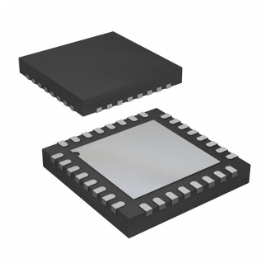
CDCLVC1310
www.ti.com
SCAS917E – JULY 2011 – REVISED JANUARY 2014
Ten-Output Low-Jitter Low-Power Clock Buffer and Level Translator
Check for Samples: CDCLVC1310
FEATURES
APPLICATIONS
•
•
•
•
•
•
1
•
•
•
•
•
•
High-Performance Crystal Buffer With Ultralow
Noise Floor of –169 dBc/Hz
Additive Phase Noise/Jitter Performance Is
25 fsRMS (Typ.)
Level Translation With 3.3-V or 2.5-V Core and
3.3-V, 2.5-V, 1.8-V, or 1.5-V Output Supply
Device inputs consist of primary, secondary,
and crystal inputs, and manually selectable
(through pins) using the input MUX. The
primary and secondary inputs can accept
LVPECL, LVDS, HCSL, SSTL or LVCMOS
signals and crystal input.
– Crystal Frequencies Supported Are From
8 MHz to 50 MHz
– Differential and Single-Ended Input
Frequencies Supported Are up to 200 MHz
10 Single-Ended LVCMOS Outputs. The
outputs can operate at 1.5-V, 1.8-V, 2.5-V or
3.3-V Power-Supply Voltage.
– LVCMOS Outputs Operate up to 200 MHz
– Output Skew Is 30 ps (Typical)
– Total Propagation Delay Is 2 ns (Typical)
– Synchronous and Glitch-Free Output
Enable Is Available
Offered in QFN-32 5-mm × 5-mm Package With
Industrial Temperature Range of –40°C to 85°C
Can Overdrive Crystal Input With LVCMOS
Signal up to 50 MHz
Wireless and Wired Infrastructure
Networking and Data Communications
Medical Imaging
Portable Test and Measurement
High-End A/V
DESCRIPTION
The CDCLVC1310 is a highly versatile, low-jitter, lowpower clock fanout buffer which can distribute to ten
low-jitter LVCMOS clock outputs from one of three
inputs, whose primary and secondary inputs can
feature differential or single-ended signals and crystal
input. Such a buffer is good for use in a variety of
mobile and wired infrastructure, data communication,
computing, low-power medical imaging, and portable
test and measurement applications. When the input is
an illegal level, the output is at a defined state. One
can set the core to 2.5 V or 3.3 V, and output to 1.5
V, 1.8 V, 2.5 V or 3.3 V. Pin programming easily
configures the CDCLVC1310. The overall additive
jitter performance is 25 fsRMS (typical). The
CDCLVC1310 comes in a small 32-pin 5-mm × 5-mm
QFN package.
1
Please be aware that an important notice concerning availability, standard warranty, and use in critical applications of
Texas Instruments semiconductor products and disclaimers thereto appears at the end of this data sheet.
PRODUCTION DATA information is current as of publication date.
Products conform to specifications per the terms of the Texas
Instruments standard warranty. Production processing does not
necessarily include testing of all parameters.
Copyright © 2011–2014, Texas Instruments Incorporated
�CDCLVC1310
SCAS917E – JULY 2011 – REVISED JANUARY 2014
www.ti.com
These devices have limited built-in ESD protection. The leads should be shorted together or the device placed in conductive foam
during storage or handling to prevent electrostatic damage to the MOS gates.
BLOCK DIAGRAM
IN_SEL0/
IN_SEL1
vDD
vDD
Differential/
LVCMOS
LVCMOS
XTAL
OSC
Input
OE
Synch Control
CDCLVC1310
Output
Figure 1. High-Level Block Diagram of CDCLVC1310
2
Submit Documentation Feedback
Copyright © 2011–2014, Texas Instruments Incorporated
Product Folder Links: CDCLVC1310
�CDCLVC1310
www.ti.com
SCAS917E – JULY 2011 – REVISED JANUARY 2014
PINOUT DIAGRAM
GND
OE
IN_SEL0
IN_SEL1
SEC_INP
SEC_INN
GND
GND
CDCLVC1310
RHB-32 Package
(Top View)
32
31
30
29
28
27
26
25
24
Y0
1
VDDO
2
23
VDDO
Y1
3
22
Y8
GND
4
21
GND
Thermal Pad
Y9
Y3
7
18
Y6
Y4
8
Y5
9
10
11
12 13
14
15
17
16
GND
VDDO
GND
19
PRI_INN
6
PRI_INP
VDDO
XOUT
Y7
XIN
20
VDD
5
GND
Y2
P0048-18
Submit Documentation Feedback
Copyright © 2011–2014, Texas Instruments Incorporated
Product Folder Links: CDCLVC1310
3
�CDCLVC1310
SCAS917E – JULY 2011 – REVISED JANUARY 2014
www.ti.com
PIN FUNCTIONS
PIN
I/O
TYPE
4, 9, 15,
16, 21,
25, 26,
32
PWR
Analog
Power-supply ground
30, 29
I
Digital
Input-clock selection (pulldown of 150 kΩ)
OE
31
I
Digital
LVCMOS output enable (pulldown of 150 kΩ)
PRI_INN
14
I
Analog
Inverting differential primary reference input, internally biased to Vdd / 2 (pullup or
pulldown of 150 kΩ)
PRI_INP
13
I
Analog
Non-inverting differential or single-ended primary reference input (pulldown of 150 kΩ)
SEC_INN
27
I
Analog
Inverting differential secondary reference input, internally biased to Vdd / 2 (pullup or
pulldown of 150 kΩ)
SEC_INP
28
I
Analog
Non-inverting differential or single-ended secondary reference input (pulldown of 150 kΩ)
NAME
NO(s)
GND
IN_SEL0,
IN_SEL1
VDD
DESCRIPTION
10
PWR
Analog
Power-supply pins
2, 6, 19,
23
PWR
Analog
I/O power-supply pins
XIN
11
I
Analog
Crystal-oscillator input or XTAL bypass mode
XOUT
12
I
Analog
Crystal-oscillator output
Y0
1
O
Analog
LVCMOS output 0
Y1
3
O
Analog
LVCMOS output 1
Y2
5
O
Analog
LVCMOS output 2
Y3
7
O
Analog
LVCMOS output 3
Y4
8
O
Analog
LVCMOS output 4
Y5
17
O
Analog
LVCMOS output 5
Y6
18
O
Analog
LVCMOS output 6
Y7
20
O
Analog
LVCMOS output 7
Y8
22
O
Analog
LVCMOS output 8
Y9
24
O
Analog
LVCMOS output 9
VDDO
Table 1. Input Selection
(1)
(2)
IN_SEL1
IN_SEL0
INPUT CHOSEN
0
0
PRI_IN
0
1
SEC_IN
1
0
XTAL or overdrive (1)
1
1
XTAL bypass (2)
This mode is for XTAL input or overdrive of XTAL oscillator with
LVCMOS input. For characteristics; see LVCMOS OUTPUT
CHARACTERISTICS.
This mode is only XTAL bypass. For characteristics, see LVCMOS
OUTPUT CHARACTERISTICS.
Table 2. INPUT/OUTPUT OPERATION (1)
(1)
4
INPUT STATE
OUTPUT STATE
PRI_INx, SEC_INx open
Logic LOW
PRI_INP, SEC_INP = HIGH,
PRI_INN, SEC_INN = LOW
Logic HIGH
PRI_INP, SEC_INP = LOW,
PRI_INN, SEC_INN = HIGH
Logic LOW
Device must have switching edge to obtain output states.
Submit Documentation Feedback
Copyright © 2011–2014, Texas Instruments Incorporated
Product Folder Links: CDCLVC1310
�CDCLVC1310
www.ti.com
SCAS917E – JULY 2011 – REVISED JANUARY 2014
Table 3. OE Function
OE
Yx
0
High-impedance
1
Enabled
ABSOLUTE MAXIMUM RATINGS (1)
over operating free-air temperature range (unless otherwise noted)
VDD,
VDDO
Supply-voltage range
VIN
Input-voltage range
VOUT
Output-voltage range
IIN
IOUT
Tstg
Storage-temperature range
TJ
Junction temperature
(1)
VALUE
UNIT
–0.5 to 4.6
V
–0.5 to VDD + 0.5
V
–0.5 to VDDO + 0.5
V
Input current
±20
V
Output current
±50
V
–65 to 150
°C
125
°C
Stresses beyond those listed under Absolute Maximum Ratings may cause permanent damage to the device. These are stress ratings
only, and functional operation of the device at these or any other conditions beyond those indicated under Recommended Operating
Conditions is not implied. Exposure to absolute-maximum-rated conditions for extended periods may affect device reliability.
RECOMMENDED OPERATING CONDITIONS
over operating free-air temperature range (unless otherwise noted)
VDDO
Output supply voltage
MIN
NOM
MAX
3.135
3.3
3.465
2.375
2.5
2.625
1.6
1.8
2
1.35
1.5
1.65
3.135
3.3
3.465
2.375
2.5
2.625
UNIT
V
VDD
Core supply voltage
IOH
High-level output current, LVCMOS
–24
mA
IOL
Low-level output current, LVCMOS
24
mA
TA
Ambient temperature
85
°C
–40
V
Submit Documentation Feedback
Copyright © 2011–2014, Texas Instruments Incorporated
Product Folder Links: CDCLVC1310
5
�CDCLVC1310
SCAS917E – JULY 2011 – REVISED JANUARY 2014
www.ti.com
THERMAL INFORMATION
CDCLVC1310
THERMAL METRIC (1)
RHB
UNIT
32 PINS
Junction-to-ambient thermal resistance (2)
θJA
(3)
41.7
°C/W
θJCtop
Junction-to-case (top) thermal resistance
34.1
°C/W
θJB
Junction-to-board thermal resistance (4)
14.4
°C/W
ψJT
Junction-to-top characterization parameter (5)
0.9
°C/W
14.4
°C/W
6.2
°C/W
(6)
ψJB
Junction-to-board characterization parameter
θJCbot
Junction-to-case (bottom) thermal resistance (7)
(1)
(2)
(3)
(4)
(5)
(6)
(7)
For more information about traditional and new thermal metrics, see the IC Package Thermal Metrics application report, SPRA953.
The junction-to-ambient thermal resistance under natural convection is obtained in a simulation on a JEDEC-standard, high-K board, as
specified in JESD51-7, in an environment described in JESD51-2a.
The junction-to-case (top) thermal resistance is obtained by simulating a cold plate test on the package top. No specific JEDECstandard test exists, but a close description can be found in the ANSI SEMI standard G30-88.
The junction-to-board thermal resistance is obtained by simulating in an environment with a ring cold plate fixture to control the PCB
temperature, as described in JESD51-8.
The junction-to-top characterization parameter, ψJT, estimates the junction temperature of a device in a real system and is extracted
from the simulation data for obtaining θJA, using a procedure described in JESD51-2a (sections 6 and 7).
The junction-to-board characterization parameter, ψJB, estimates the junction temperature of a device in a real system and is extracted
from the simulation data for obtaining θJA , using a procedure described in JESD51-2a (sections 6 and 7).
The junction-to-case (bottom) thermal resistance is obtained by simulating a cold plate test on the exposed (power) pad. No specific
JEDEC standard test exists, but a close description can be found in the ANSI SEMI standard G30-88.
Spacer
INPUT CHARACTERISTICS
over recommended ranges of supply voltage (VDDO ≤ VDD), load and ambient temperature (unless otherwise noted)
PARAMETER
TEST CONDITIONS
MIN
TYP
MAX
UNIT
DC Characteristic (OE, IN_SEL0, IN_SEL1, PRI_IN, SEC_IN)
IIH
Input high current
VDD = 3.465 V, VIH = 3.465 V
IIL
Input low current
VDD = 3.465 V, VIL= 0 V
ΔV/ΔT
Input edge rate
20%–80%
40
–40
2
RPullup/down Pullup or pulldown resistance
CIN
Input capacitance
µA
µA
V/ns
150
kΩ
2
pF
Single-Ended DC Characteristic (PRI_INP, SEC_INP) (1)
VIH
Input high voltage
VIL
Input low voltage
VDD = 3.3 V ±5%
2
VDD + 0.3
VDD = 2.5 V ±5%
1.6
VDD + 0.3
VDD = 3.3 V ±5%
–0.3
1.3
VDD = 2.5 V ±5%
–0.3
0.9
V
V
Single-Ended DC Characteristic (OE, IN_SEL0, IN_SEL1)
VIH
Input high voltage
VIL
Input low voltage
0.7 × VDD
V
0.3 × VDD
V
0.15
1.3
V
0.5
VDD – 0.85
V
Differential DC Characteristic (PRI_IN, SEC_IN)
VI,DIFF
Differential input voltage swing (2)
VICM
Input common-mode voltage (3)
AC Characteristic (PRI_IN, SEC_IN)
fIN
Input frequency
DC
200
idc
Input duty cycle
40%
60%
(1)
(2)
(3)
6
MHz
PRI/SEC_INN biased to VDD / 2
VIL should not be less than –0.3 V
Input common-mode voltage is defined as VIH (see Figure 19).
Submit Documentation Feedback
Copyright © 2011–2014, Texas Instruments Incorporated
Product Folder Links: CDCLVC1310
�CDCLVC1310
www.ti.com
SCAS917E – JULY 2011 – REVISED JANUARY 2014
CRYSTAL CHARACTERISTICS
over recommended ranges of supply voltage, load and ambient temperature (unless otherwise noted)
PARAMETER
TEST CONDITIONS
MIN
TYP
Equivalent series resistance (ESR)
Maximum shunt capacitance
Drive level
MAX
UNIT
50
Ω
7
pF
100
µW
CRYSTAL OSCILLATOR CHARACTERISTICS
over recommended ranges of supply voltage, load and ambient temperature (unless otherwise noted)
PARAMETER
TEST CONDITIONS
MIN
Mode of oscillation
TYP
Frequency
8
Frequency in overdrive mode
(1)
Frequency in bypass mode (2)
On-chip load capacitance
(1)
(2)
MAX
UNIT
50
MHz
50
MHz
50
MHz
Fundamental
12
pF
Input signal swing (max) = 2 V; input signal tr (max) = 10 ns; tf(max) = 10 ns; functional, but device may not meed ac parameters.
Input signal swing (max) = VDD; input signal tr (max) = 10 ns; tf(max) = 10 ns; functional, but device may not meed ac parameters.
LVCMOS OUTPUT CHARACTERISTICS
over recommended ranges of supply voltage (VDDO ≤ VDD), load (50 Ω to VDDO/2), and ambient temperature (unless
otherwise noted)
PARAMETER
TEST CONDITIONS
MIN
TYP
fOUT
VOH
VDDO = 3.135 V to 3.465 V
0.8 *
VDDO
VDDO = 2.375 V to 2.625 V
0.8 *
VDDO
VDDO = 1.6 V to 2 V
0.7 *
VDDO
VDDO = 1.35 V to 1.65 V
0.7 *
VDDO
Output high voltage
VOL
Output impedance
Output slew rate, rising and falling
tSK
Output skew
tSK,PP
(1)
Part-to-part skew
MHz
VDDO = 3.135 V to 3.465 V
0.2 *
VDDO
VDDO = 2.375 V to 2.625 V
0.2 *
VDDO
VDDO = 1.6 V to 2 V
0.3 *
VDDO
VDDO = 1.35 V to 1.65 V
0.3 *
VDDO
VDDO = 3.3 V
15
VDDO = 2.5 V
20
VDDO = 1.8 V
25
VDDO = 1.5 V
tSLEW-RATE
UNIT
200
V
Output low voltage
ROUT
MAX
V
Ω
30
VDDO=3.3V +/- 5%, 20% to 80%
5.6
7.3
9.0
VDDO=2.5V +/- 5%, 20% to 80%
3.9
4.8
5.4
VDDO=1.8V +/- 200mV, 20% to 80%
1.6
2.1
2.5
VDDO=1.5V +/- 150mV, 20% to 80%
0.9
1.2
1.4
30
50
ps
2
ns
(1)
V/ns
Calculation for part-to-part skew is the difference between the fastest and the slowest tpd across multiple devices.
Submit Documentation Feedback
Copyright © 2011–2014, Texas Instruments Incorporated
Product Folder Links: CDCLVC1310
7
�CDCLVC1310
SCAS917E – JULY 2011 – REVISED JANUARY 2014
www.ti.com
LVCMOS OUTPUT CHARACTERISTICS (continued)
over recommended ranges of supply voltage (VDDO ≤ VDD), load (50 Ω to VDDO/2), and ambient temperature (unless
otherwise noted)
PARAMETER
tDELAY
TEST CONDITIONS
Output frequency
tRJIT
System-level additive jitter
(2)
MIN
TYP
MAX
VDD = 3.3 V ±5%,
VDDO = 1.35 V to VDD
1.5
1.95
4.0
VDD = 2.5 V ±5%,
VDDO = 1.35 V to VDD
1.8
2.4
4.4
NF
Noise floor
25
Single-ended input, VDD = 2.5 V or
3.3 V, VDDO = 1.5 V, 1.8 V, or 2.5 V,
fIN/OUT = 125 MHz
30
Differential input, VDD = 3.3 V,
VDDO = 3.3 V
30
Differential input, VDD = 2.5 V or
3.3 V, VDDO = 1.5 V, 1.8 V, or 2.5 V,
fIN/OUT = 125 MHz
30
–145
100-kHz offset (3)
–156
(3)
tEN
Output enable or disable time
MUXISOLATION
(2)
(3)
(4)
(5)
(6)
8
MUX isolation
(6)
–163
10-MHz offset (3)
–164
20-MHz offset (3)
–164
(4)
dBc/Hz
–145
100-kHz offset (4)
–155
1-MHz offset (4)
–160
10-MHz offset (4)
–161
20-MHz offset
Output duty cycle
fS, RMS
10-kHz offset (3)
10-kHz offset
odc
ns
Single-ended input, VDD = 3.3 V,
VDDO = 3.3 V
1-MHz offset
(4)
–162
fIN/OUT = 125 MHz, idc = 50% (5)
45%
55%
2
125 MHz
UNIT
55
Cycle
dB
Integration range: 12 kHz–20 MHz; input source see the System-Level Additive-Jitter Measurement section
Single-ended input, fIN/OUT = 125 MHz, VDD = VDDO = 3.3 V
Differential input, fIN/OUT = 125 MHz, VDD = VDDO = 3.3 V
Stable VIH, VIL, and VCM
See Figure 18.
Submit Documentation Feedback
Copyright © 2011–2014, Texas Instruments Incorporated
Product Folder Links: CDCLVC1310
�CDCLVC1310
www.ti.com
SCAS917E – JULY 2011 – REVISED JANUARY 2014
PHASE NOISE WITH XTAL (1) SELECTED
VDD = VDDO = 2.5 V or 3.3 V, fXTAL = 25 MHz, TA = 25°C (unless otherwise noted)
PARAMETER
Jrms
TEST CONDITIONS
RMS phase jitter
MIN
TYP
IB = 12 kHz to 5 MHz, VDD = VDDO = 3.3 V
80
IB = 12 kHz to 5 MHz, VDD = VDDO = 2.5 V
115
foffset = 100 Hz, VDD = VDDO = 3.3 V
PN
(1)
Phase noise (see Figure 15)
MAX
UNIT
fs rms
–92
foffset = 1 kHz, VDD = VDDO = 3.3 V
–137
foffset = 10 kHz, VDD = VDDO = 3.3 V
–163
foffset = 100 kHz, VDD = VDDO = 3.3 V
–168
foffset = 1 MHz, VDD = VDDO = 3.3 V
–168
foffset = 5 MHz, VDD = VDDO = 3.3 V
–169
foffset = 100 Hz, VDD = VDDO = 2.5 V
–91
foffset = 1 kHz, VDD = VDDO = 2.5 V
–136
foffset = 10 kHz, VDD = VDDO = 2.5 V
–159
foffset = 100 kHz, VDD = VDDO = 2.5 V
–164
foffset = 1 MHz, VDD = VDDO = 2.5 V
–165
foffset = 5 MHz, VDD = VDDO = 2.5 V
–165
dBc/Hz
Crystal specification: CL = 18 pF; ESR = 35 Ω (max); C0 = 7 pF; drive level = 100 µW (max)
DEVICE CURRENT CONSUMPTION
over recommended ranges of supply voltage, load and ambient temperature (unless otherwise noted)
PARAMETER
TEST CONDITIONS
MIN
TYP
MAX
UNIT
OVERALL PARAMETERS FOR ALL VERSIONS
IDD
Static device current
IDD,XTAL
CPD
(1)
(2)
(1)
OE = 0 V or VDD;
Ref. input (PRI/SEC) = 0 V or VDD;
IO = 0 mA; VDD / VDDO = 3.3 V
14
OE = 0 V or VDD;
Ref. input (PRI/SEC) = 0 V or VDD;
IO = 0 mA; VDD / VDDO = 2.5 V
8
mA
Device current with XTAL
input (1)
Power dissipation capacitance
per output (2)
20
mA
VDDO = 3.465 V; f = 100 MHz
8.8
VDDO = 2.625 V; f = 100 MHz
7.7
VDDO = 2 V; f = 100 MHz
7.3
VDDO = 1.65 V; f = 100 MHz
6.9
pF
IDD and IDD,XTAL is the current through VDD; outputs enabled or in the high-impedance state; no load.
This is the formula for the power dissipation calculation (see the Power Considerations section)
IDD,Total = IDD + IDD,Cload + IDD,dyn [mA]
IDD,dyn = CPD × VDDO × f × n [mA]
IDD,Cload = Cload × VDDO × f × n [mA]
n = Number of switching output pins
Submit Documentation Feedback
Copyright © 2011–2014, Texas Instruments Incorporated
Product Folder Links: CDCLVC1310
9
�CDCLVC1310
SCAS917E – JULY 2011 – REVISED JANUARY 2014
www.ti.com
TEST CONFIGURATIONS
Figure 2 through Figure 8 illustrate how to set up the device for a variety of test configurations.
+ VDDO/2
LVCMOS
output
ZO = 50 W
R=50 W from
measurement
equipment
– VDDO/2
Figure 2. LVCMOS Output DC Configuration; Test Load Circuit
VDD
VDD
VDD
R = 100 W
R=1kW
Rs
x_INP
Zo = 50 W
Zo
x_INN
R = 100 W
R=1kW
C = 0.1 mF
Clock generator:
Zo + Rs = 50 W
Figure 3. LVCMOS Input DC Configuration During Device Test
VDD
VDD
VDD
R = 125 W
R = 125 W
Zo = 50 W
x_INP
LVPECL
output
x_INN
Zo = 50 W
R = 84 W
R = 84 W
Figure 4. LVPECL Input Configuration During Device Test
10
Submit Documentation Feedback
Copyright © 2011–2014, Texas Instruments Incorporated
Product Folder Links: CDCLVC1310
�CDCLVC1310
www.ti.com
SCAS917E – JULY 2011 – REVISED JANUARY 2014
VDD
VDD
Zo = 50 W
x_INP
LVPECL
output
x_INN
Zo = 50 W
R = 50 W
R = 50 W
R = 50 W
Figure 5. LVPECL Input Configuration During Device Test
VDD
VDD
R = 33 W
Zo = 50 W
x_INP
HCSL
output
x_INN
Zo = 50 W
R = 33 W
R = 50 W
R = 50 W
Figure 6. HCSL Input Configuration During Device Test
VDD
VDD
Zo = 50 W
x_INP
LVD
output
R = 100 W
x_INN
Zo = 50 W
Figure 7. LVDS Input Configuration During Device Test
Submit Documentation Feedback
Copyright © 2011–2014, Texas Instruments Incorporated
Product Folder Links: CDCLVC1310
11
�CDCLVC1310
SCAS917E – JULY 2011 – REVISED JANUARY 2014
www.ti.com
VDD
VDD
VDD
R = 120 W
R = 120 W
Zo = 60 W
x_INP
SSTL
output
x_INN
Zo = 60 W
R = 120 W
R = 120 W
Figure 8. SSTL Input Configuration During Device Test
12
Submit Documentation Feedback
Copyright © 2011–2014, Texas Instruments Incorporated
Product Folder Links: CDCLVC1310
�CDCLVC1310
www.ti.com
SCAS917E – JULY 2011 – REVISED JANUARY 2014
APPLICATION INFORMATION
Typical Application Load
VDDO
RS » 35 W, 30 W, 20 W, 10 W
(VDDO = 3.3 V, 2.5 V, 1.8 V, 1.5 V)
LVC1310
output
LVCMOS
input
ZO = 50 W
10 pF
Figure 9. LVCMOS Output DC Configuration: Typical Application Load
Parameter Measurement Information
80%
Yx
0V
VOUT
20%
tR
tF
Figure 10. LVCMOS Output Voltage, and Rise and Fall Times
PRI_IN/SEC_IN
LVCMOS
PRI_IN/SEC_IN (N)
Differential
PRI_IN/SEC_IN (P)
tPD
Yx
LVCMOS
tSK
Yy
LVCMOS
Figure 11. Differential and Single-Ended Output Skew and Propagation Delay
Crystal Oscillator Input
The crystal oscillator circuit is characterized with 18-pF parallel-resonant crystals. Choices of C1 and C2 were to
minimize the ppm error. Optional resistor ROPTIONAL limits the drive level of the oscillator circuit.
Submit Documentation Feedback
Copyright © 2011–2014, Texas Instruments Incorporated
Product Folder Links: CDCLVC1310
13
�CDCLVC1310
SCAS917E – JULY 2011 – REVISED JANUARY 2014
www.ti.com
ROPTIONAL
Crystal
XIN
C1
XOUT
C2
Figure 12. Crystal Reference Input
The input XIN can accept single-ended LVCMOS signals in two configurations. It is possible to overdrive the
oscillator stage or to use a pure LVCMOS input (see Table 1). If overdriving the oscillator stage, it is necessary
to ac-couple the input with a capacitor (see Figure 13). Otherwise, if selecting the bypass, there is no
requirement for a coupling capacitor. Additional measurements and information about crystal oscillator input and
limiting the drive level are available in the applications report Crystal Oscillator Performance of the CDCLVC1310
(SCAA119).
NOTE
If using the overdrive or bypass mode, the device is functional, but may not meet its ac
parameters.
VDD
VDD
R1 = 100 W
Rs
RINT
XIN
Zo = 50 W
C = 0.1 mF
XOUT
R2 = 100 W
Clock Generator:
RINT + Rs = 50 W
Figure 13. Single-Ended Crystal Input
Phase-Noise Performance
The CDCLVC1310 provides ultralow phase-noise outputs (noise floor = –170 dBc/Hz) if it has an attached
crystal. Figure 14 shows the phase-noise plot of the CDCLVC1310 with a 25-MHz crystal at VDD = VDDO = 3.3 V
and room temperature.
14
Submit Documentation Feedback
Copyright © 2011–2014, Texas Instruments Incorporated
Product Folder Links: CDCLVC1310
�CDCLVC1310
www.ti.com
SCAS917E – JULY 2011 – REVISED JANUARY 2014
Figure 14. Phase-Noise Profile With 25-MHz Crystal at Nominal Conditions
System-Level Additive-Jitter Measurement
For high-performance devices, limitations of the equipment influence phase-noise measurements. The noise floor
of the equipment often exceeds the noise floor of the device. The real noise floor of the device is probably lower
(see LVCMOS Output Characteristics). Phase noise is influenced by the input source and the measurement
equipment. Additional measurements and information about system-level additive jitter and noise floor are
available in the applications report Phase Noise Performance of CDCLVC1310 (SCAA115).
Submit Documentation Feedback
Copyright © 2011–2014, Texas Instruments Incorporated
Product Folder Links: CDCLVC1310
15
�CDCLVC1310
SCAS917E – JULY 2011 – REVISED JANUARY 2014
www.ti.com
Figure 15. Input Phase Noise (179.4 fs, Light Blue) and Output Phase Noise (180 fs, Dark Blue)
Output Enable
Pulling OE to LOW (t1), forces the outputs to the high-impedance state after the next falling edge of the input
signal (t2). The outputs remain in the high-impedance state as long as OE is LOW (see Figure 16).
X_INN
Differential Input
X_INP
SE Input
X_INP
Output Enable OE
Output Yx
t1
t2
Figure 16. OE: Disable Outputs
16
Submit Documentation Feedback
Copyright © 2011–2014, Texas Instruments Incorporated
Product Folder Links: CDCLVC1310
�CDCLVC1310
www.ti.com
SCAS917E – JULY 2011 – REVISED JANUARY 2014
If the outputs are in the high-impedance state, pulling OE to HIGH forces all outputs LOW asynchronously (t3).
Within two clock cycles (maximum), the outputs start switching again (t4), after a falling edge of the input signal
(see Figure 17).
X_INP
Differential input
X_INN
or
X_INP
SE input
Output enable OE
Output Yx
t3
t4
Figure 17. OE: Enable Outputs
If the outputs are in the high-impedance state and the input is static (no clock signal), OE works fully
asynchronously. A transition of OE from LOW to HIGH forces the outputs to LOW. A transition from HIGH to
LOW does not force to the high-impedance state again. Therefore, a state change requires a falling edge of the
input signal (see Figure 16).
MUX Isolation
Amplitude [dB]
The definition of MUX isolation is the difference in output amplitude (dB) between an active and a static input
signal.
Yx, if MUX selects active input signal
MUX isolation
Yx, if MUX selects static input signal
fcarrier
Frequency [MHz]
Figure 18. Output Spectrum of an Active and a Static Input Signal
Submit Documentation Feedback
Copyright © 2011–2014, Texas Instruments Incorporated
Product Folder Links: CDCLVC1310
17
�CDCLVC1310
SCAS917E – JULY 2011 – REVISED JANUARY 2014
www.ti.com
Differential Input Level
VDD
X_INN
VI,DIFF
VICM = VIH
X_INP
VCM
GND
NOTE: The calculation for VCM is: VCM = VDD – VICM – VI,DIFF/2
Figure 19. Differential Input Level
Power Considerations
The following power consideration refers to the device-consumed power consumption only. The device power
consumption is the sum of static power and dynamic power. The dynamic power usage consists of two
components:
• Power used by the device as it switches states
• Power required to charge any output load
The output load can be capacitive-only or capacitive and resistive. Use the following formula to calculate the
power consumption of the device:
PDev = Pstat + Pdyn + PCload (see Figure 20 and Figure 21)
Pstat = IDD × VDD
Pdyn + PCload = (IDD,dyn + IDD,Cload) × VDDO
where:
IDD,dyn = CPD × VDDO × f × n [mA] (see Figure 22)
IDD,Cload = Cload × VDDO × f × n [mA]
Example for power consumption of the CDCLVC1310: 10 outputs are switching, f = 100 MHz, VDD = VDDO = 3.3
V and assuming Cload = 2 pF per output:
PDev = 46.2 mW + 117.5 mW = 163.7 mW
Pstat = 14 mA × 3.3 V = 46.2 mW
Pdyn + PCload = (29 mA + 6.6 mA) x 3.3 V = 117.5 mW
IDD,dyn = 8.8 pF × 3.3 V × 100 MHz × 10 = 29 mA
IDD,Cload = 2 pF × 3.3 V x 100 MHz × 10 = 6.6 mA
NOTE
For dimensioning the power supply, consider the total power consumption. The total
power consumption is the sum of device power consumption and the power consumption
of the load.
18
Submit Documentation Feedback
Copyright © 2011–2014, Texas Instruments Incorporated
Product Folder Links: CDCLVC1310
�CDCLVC1310
www.ti.com
SCAS917E – JULY 2011 – REVISED JANUARY 2014
VDD=VDDO=2.625V
16
Device Power Consumption (mW)
14
12
10
8
Pstat + Pdyn + PCload2pF
Pstat + Pdyn + PCload8pF
6
4
0
Figure 20. Device Power Consumption versus
Clock Frequency (VDD = VDDO = 3.465 V; Load
2 pF, 8 pF; per Output)
Idyn − Dynamic Supply Current (mA)
6
20
40
60
80 100 120 140
f − Clock Frequency (MHz)
160
180
200
Figure 21. Device Power Consumption versus
Clock Frequency (VDD = VDDO = 2.625 V; Load
2 pF, 8 pF; per Output)
VDDO=3.465V
VDDO=2.625V
VDDO=2.0V
VDDO=1.65V
5
4
3
2
1
0
0
20
40
60
80 100 120 140
f − Clock Frequency (MHz)
160
180
200
Figure 22. Dynamic Supply Current versus Clock Frequency (per Output)
Submit Documentation Feedback
Copyright © 2011–2014, Texas Instruments Incorporated
Product Folder Links: CDCLVC1310
19
�CDCLVC1310
SCAS917E – JULY 2011 – REVISED JANUARY 2014
www.ti.com
Thermal Management
Power consumption of the CDCLVC1310 can be high enough to require attention to thermal management. For
reliability and performance reasons, limit the die temperature to a maximum of 125°C. That is, as an estimate, TA
(ambient temperature) plus device power consumption times θJA should not exceed 125°C.
The device package has an exposed pad that provides the primary heat removal path as well as an electrical
grounding to the printed circuit board (PCB). To maximize the removal of heat from the package, incorporate a
thermal landing pattern including multiple vias to a ground plane on the PCB within the footprint of the package.
Solder the exposed pad down to ensure adequate heat conduction out of the package. Figure 23 shows a
recommended land and via pattern.
3.0 mm
(min)
0.3 mm
(typ)
0.7 mm
(typ)
Figure 23. Recommended PCB Layout for CDCLVC1310
20
Submit Documentation Feedback
Copyright © 2011–2014, Texas Instruments Incorporated
Product Folder Links: CDCLVC1310
�CDCLVC1310
www.ti.com
SCAS917E – JULY 2011 – REVISED JANUARY 2014
Power-Supply Filtering
High-performance clock buffers are sensitive to noise on the power supply, which can dramatically increase the
additive jitter of the buffer. Thus, it is essential to reduce noise from the system power supply, especially when
jitter or phase noise is very critical to applications.
Use of filter capacitors eliminates the low-frequency noise from power supply, where the bypass capacitors
provide the very low-impedance path for high-frequency noise and guard the power-supply system against
induced fluctuations. The bypass capacitors also provide instantaneous current surges as required by the device,
and should have low ESR. To use the bypass capacitors properly, place them very close to the power supply
pins and lay out traces with short loops to minimize inductance. TI recommends to adding as many highfrequency (for example, 0.1-µF) bypass capacitors as there are supply pins in the package. There is a
recommendation, but not a requirement, to insert a ferrite bead between the board power supply and the chip
power supply to isolate the high-frequency switching noises generated by the clock driver, preventing them from
leaking into the board supply. Choosing an appropriate ferrite bead with very low dc resistance is important,
because it is imperative to provide adequate isolation between the board supply and the chip supply, and to
maintain a voltage at the supply pins that is greater than the minimum voltage required for proper operation.
Board
Supply
VDD
Chip
Supply
Ferrite Bead
C
10 µF
C
1 µF
6 xC
0.1 µF
Figure 24. Power-Supply Decoupling
Submit Documentation Feedback
Copyright © 2011–2014, Texas Instruments Incorporated
Product Folder Links: CDCLVC1310
21
�CDCLVC1310
SCAS917E – JULY 2011 – REVISED JANUARY 2014
www.ti.com
REVISION HISTORY
Changes from Revision D (July 2013) to Revision E
Page
•
Changed VOH in LVCMOS OUTPUT CHARACTERISTICS ................................................................................................. 7
•
Changed VOL in LVCMOS OUTPUT CHARACTERISTICS .................................................................................................. 7
•
Changed tSLEW-RATE in LVCMOS OUTPUT CHARACTERISTICS ......................................................................................... 7
Changes from Revision C (October 2012) to Revision D
•
Page
Changed tDELAY in LVCMOS OUTPUT CHARACTERISTICS .............................................................................................. 8
Changes from Revision B (February 2012) to Revision C
Page
•
Changed unit for phase jitter from picosecond to femtosecond ........................................................................................... 9
•
Revised Figure 3 ................................................................................................................................................................. 10
•
Revised Figure 4 ................................................................................................................................................................. 10
•
Revised Figure 5 ................................................................................................................................................................. 11
•
Revised Figure 6 ................................................................................................................................................................. 11
•
Revised Figure 8 ................................................................................................................................................................. 12
•
Added reference to application report SCAA119 ................................................................................................................ 14
22
Submit Documentation Feedback
Copyright © 2011–2014, Texas Instruments Incorporated
Product Folder Links: CDCLVC1310
�PACKAGE OPTION ADDENDUM
www.ti.com
6-Feb-2020
PACKAGING INFORMATION
Orderable Device
Status
(1)
CDCLVC1310RHBR
ACTIVE
Package Type Package Pins Package
Drawing
Qty
VQFN
RHB
32
3000
Eco Plan
Lead/Ball Finish
MSL Peak Temp
(2)
(6)
(3)
Green (RoHS
& no Sb/Br)
NIPDAU
Level-2-260C-1 YEAR
Op Temp (°C)
Device Marking
(4/5)
-40 to 85
CDCLVC
1310
(1)
The marketing status values are defined as follows:
ACTIVE: Product device recommended for new designs.
LIFEBUY: TI has announced that the device will be discontinued, and a lifetime-buy period is in effect.
NRND: Not recommended for new designs. Device is in production to support existing customers, but TI does not recommend using this part in a new design.
PREVIEW: Device has been announced but is not in production. Samples may or may not be available.
OBSOLETE: TI has discontinued the production of the device.
(2)
RoHS: TI defines "RoHS" to mean semiconductor products that are compliant with the current EU RoHS requirements for all 10 RoHS substances, including the requirement that RoHS substance
do not exceed 0.1% by weight in homogeneous materials. Where designed to be soldered at high temperatures, "RoHS" products are suitable for use in specified lead-free processes. TI may
reference these types of products as "Pb-Free".
RoHS Exempt: TI defines "RoHS Exempt" to mean products that contain lead but are compliant with EU RoHS pursuant to a specific EU RoHS exemption.
Green: TI defines "Green" to mean the content of Chlorine (Cl) and Bromine (Br) based flame retardants meet JS709B low halogen requirements of