User's Guide
SCAU044 – July 2010
Low-Additive Jitter, Four-LVDS-Outputs Clock Buffer With
Divider EVM
This user's guide describes how to use the CDCLVD1213 evaluation module (EVM) and provides users
with guidelines to build their own systems. The EVM schematics and bill of materials are included.
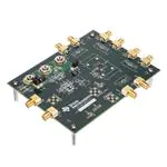
Figure 1. CDCLVD1213 Evaluation Board
1
Features
•
•
•
•
•
•
•
1.1
Easy-to-use evaluation board to fan out low-phase noise clocks
Easy device setup
Fast configuration
Control pin configurable through jumpers
Board powered at 2.5 V
Differential input clocks
Device and EVM support four LVDS outputs
General Description
The CDCLVD1213 is a high-performance, low-additive jitter clock buffer with divider. The device has one
differential input with internal 140-Ω differential input termination.
SCAU044 – July 2010
Low-Additive Jitter, Four-LVDS-Outputs Clock Buffer With Divider EVM
Copyright © 2010, Texas Instruments Incorporated
1
�Getting Started
www.ti.com
The evaluation module (EVM) is designed to demonstrate the electrical performance of the CDCLVD1213.
This fully assembled and factory-tested evaluation board allows complete validation of device
functionalities. For optimum performance, the board is equipped with SMA connectors and well-controlled
50-Ω impedance microstrip transmission lines.
1.2
Signal Path and Control Circuitry
The CDCLVD1213 supports differential input up to 800 MHz. Each device provides up to three LVDS
outputs operating at the input frequency and one output with divide by /1, /2, or /4 frequency.
For more information, see the CDCLVD1213 product data sheet (SCAS897) for details.
2
Getting Started
The EVM has self-explanatory labeling and offers almost the same naming convention as used in the data
sheet. All words appearing in bold italic print in this document are the actual labeling on the EVM.
3
Power Supply Connection
Connect the power supply source to the banana plug labeled VDD2.5V (P3), and connect the ground of
the power supply source to the GND (P2). Place the jumpers between 2 and 3 for JP6 and JP7. Ensure
that LED D2 and D3 are on.
Decoupling capacitors and ferrite beads isolate the EVM power from the device’s power pins. Supply
voltage of a 2.375-V to 2.625-V range can be used in this EVM.
The EVM has an option of providing 3.3 V (P1) and an LDO to convert 3.3 V to 2.5 V. The LDO (U3) is
unpopulated on the EVM.
4
Input Clock Connection
The inputs can be applied through the SMAs, J2 and J3. These inputs are ac coupled to the device inputs
and the common-mode voltage for these inputs after the ac-coupling capacitors are provided externally by
R7 (0 Ω) and R2 and R4.
The device input has an internal 140-Ω resistor. So, for 50-Ω characteristics impedance lines, an external
350 Ω is populated at R9.
5
Output Clock
The CDCLVD1213 generates up to four LVDS outputs. Four outputs are available on the EVM through the
following SMAs: J5 and J6 for QP0; J7 and J8 for QP1; J9 and J10 for QP2; and J11 and J12 for QD.
The LVDS outputs are ac coupled to the respective SMAs. Each output pair has an option of 100-Ω
termination on the board (R23 - R26 – unpopulated).
Table 1. Divider Selection Table for QD Output
6
DIV (JP1)
Divider Ratio
0 (GND)
/1
OPEN
/2
1 (VDD2.5VMISC)
/4
Onboard Oscillator/VCO
This EVM has an option of oscillator or VCO whose output is directly connected to the inputs of the
CDCLVD12313 through R1 and R3. The oscillator (U2) and the associated components are unpopulated
on the EVM.
7
The EVM Board Schematic
Figure 2 through Figure 4 show the printed-circuit board (PCB) schematics.
2
Low-Additive Jitter, Four-LVDS-Outputs Clock Buffer With Divider EVM
Copyright © 2010, Texas Instruments Incorporated
SCAU044 – July 2010
�The EVM Board Schematic
www.ti.com
Figure 2. CDCLVD1213EVM – Schematic 1
SCAU044 – July 2010
Low-Additive Jitter, Four-LVDS-Outputs Clock Buffer With Divider EVM
Copyright © 2010, Texas Instruments Incorporated
3
�The EVM Board Schematic
www.ti.com
Figure 3. CDCLVD1213EVM – Schematic 2
4
Low-Additive Jitter, Four-LVDS-Outputs Clock Buffer With Divider EVM
Copyright © 2010, Texas Instruments Incorporated
SCAU044 – July 2010
�The EVM Board Schematic
www.ti.com
Figure 4. CDCLVD1213EVM – Schematic 3
SCAU044 – July 2010
Low-Additive Jitter, Four-LVDS-Outputs Clock Buffer With Divider EVM
Copyright © 2010, Texas Instruments Incorporated
5
�Bill of Materials
8
www.ti.com
Bill of Materials
Qty
Value
Ref Des
Footprint
Part Category
Manufacturer
Manufacturer Part #
12
0.1µF
C2, C3,
C18–C26
0402
Capacitors
Venkel
C0402X7R160-104KNE
1
100pF
C15
0402
Capacitors
Venkel
C0402COG500101JNE
1
18pF
C11
0402
Capacitors
Murata Electronics North America
GRM1555C1H180JZ01
D
1
10µF
C1
0603
Capacitors
Panasonic
ECJ-1VB0J106M
1
1.0µF
C14
0805
Capacitors
Murata Electronics North America
GRM21BR71H105KA1
2L
8
10µF
C4, C13
0805
Capacitors
Murata Electronics North America
GRM21BR71A106KE5
1L
3
1×2
JP6, JP7
0.1"
Connectors
Samtec
HTSW-150-07-G-S
4
1×3
JP1
0.1"
Connectors
Samtec
HTSW-150-07-G-S
3
Banana Plug Metal
P2, P3
4mm
Connectors
Emerson Network Power
Connectivity Solutions
108-0740-001
3
142-0701-231
RF SMA
Connectors
Emerson Network Power
Connectivity Solutions
142-0701-231
10
142-0721-881
J2, J3, J5–J12
RF SMA Edge mount
Connectors
Emerson Network Power
Connectivity Solutions
142-0721-881
2
MBRS240LT3G
D4
SMB
Semiconductor
Products
On Semiconductor
MBRS240LT3G
2
1000
L1
0603
Filters
Murata Electronics North America
BLM18HD102SN1D
1
TPS79601DRBR
U3
8-SON
Integrated Circuits
Texas Instruments
TPS79601DRBR
2
LED - Green
D2, D3
0603
Optoelectronics
Panasonic - Ssg
LNJ312G8LRA
3
0.0 (Zero Ohm)
R8
0402
Resistors
Panasonic - Ecg
ERJ-2GE0R00X
1
1.00K
R11
0402
Resistors
Venkel
CR0402-16W-1001FT
3
10.0K
R19, R20, R21
0402
Resistors
Rohm
MCR01MZPF1002
1
100
R10
0402
Resistors
Venkel
CR0402-16W-1000FT
1
30.1K
R13
0402
Resistors
Venkel
CR0402-16W-3012FT
1
30.9K
R12
0402
Resistors
Panasonic – Ecg
ERJ-2RKF3092X
1
453
R18
0402
Resistors
Panasonic – Ecg
ERJ-2RKF4530X
1
0.0 (Zero Ohm)
R22
0603
Resistors
Panasonic – Ecg
ERJ-3GEY0R00V
2
10.0K
R2, R4
0603
Resistors
Venkel
CR0603-10W-1002FT
2
301
R14, R15
0603
Resistors
Yageo America
RC0603FR-07301RL
1
CDCLVD1213
U1
16-QFN
Integrated Circuits
Texas Instruments
CDCLVD1213
1
571FCB000109D
G
U2
8-SMT
Oscillator
Silicon Labs
571FCB000109DG
10
DNI
R16, R17, R5,
R6, R9, R23–26,
R7
0402
Resistors
2
DNI
C5, C6
0402
Capacitors
1
4-PIN_PROBEDNI
J13–J17
4_17mil_100
Probe
6
Low-Additive Jitter, Four-LVDS-Outputs Clock Buffer With Divider EVM
Copyright © 2010, Texas Instruments Incorporated
SCAU044 – July 2010
�Evaluation Board/Kit Important Notice
Texas Instruments (TI) provides the enclosed product(s) under the following conditions:
This evaluation board/kit is intended for use for ENGINEERING DEVELOPMENT, DEMONSTRATION, OR EVALUATION
PURPOSES ONLY and is not considered by TI to be a finished end-product fit for general consumer use. Persons handling the
product(s) must have electronics training and observe good engineering practice standards. As such, the goods being provided are
not intended to be complete in terms of required design-, marketing-, and/or manufacturing-related protective considerations,
including product safety and environmental measures typically found in end products that incorporate such semiconductor
components or circuit boards. This evaluation board/kit does not fall within the scope of the European Union directives regarding
electromagnetic compatibility, restricted substances (RoHS), recycling (WEEE), FCC, CE or UL, and therefore may not meet the
technical requirements of these directives or other related directives.
Should this evaluation board/kit not meet the specifications indicated in the User’s Guide, the board/kit may be returned within 30
days from the date of delivery for a full refund. THE FOREGOING WARRANTY IS THE EXCLUSIVE WARRANTY MADE BY
SELLER TO BUYER AND IS IN LIEU OF ALL OTHER WARRANTIES, EXPRESSED, IMPLIED, OR STATUTORY, INCLUDING
ANY WARRANTY OF MERCHANTABILITY OR FITNESS FOR ANY PARTICULAR PURPOSE.
The user assumes all responsibility and liability for proper and safe handling of the goods. Further, the user indemnifies TI from all
claims arising from the handling or use of the goods. Due to the open construction of the product, it is the user’s responsibility to
take any and all appropriate precautions with regard to electrostatic discharge.
EXCEPT TO THE EXTENT OF THE INDEMNITY SET FORTH ABOVE, NEITHER PARTY SHALL BE LIABLE TO THE OTHER
FOR ANY INDIRECT, SPECIAL, INCIDENTAL, OR CONSEQUENTIAL DAMAGES.
TI currently deals with a variety of customers for products, and therefore our arrangement with the user is not exclusive.
TI assumes no liability for applications assistance, customer product design, software performance, or infringement of
patents or services described herein.
Please read the User’s Guide and, specifically, the Warnings and Restrictions notice in the User’s Guide prior to handling the
product. This notice contains important safety information about temperatures and voltages. For additional information on TI’s
environmental and/or safety programs, please contact the TI application engineer or visit www.ti.com/esh.
No license is granted under any patent right or other intellectual property right of TI covering or relating to any machine, process, or
combination in which such TI products or services might be or are used.
FCC Warning
This evaluation board/kit is intended for use for ENGINEERING DEVELOPMENT, DEMONSTRATION, OR EVALUATION
PURPOSES ONLY and is not considered by TI to be a finished end-product fit for general consumer use. It generates, uses, and
can radiate radio frequency energy and has not been tested for compliance with the limits of computing devices pursuant to part 15
of FCC rules, which are designed to provide reasonable protection against radio frequency interference. Operation of this
equipment in other environments may cause interference with radio communications, in which case the user at his own expense
will be required to take whatever measures may be required to correct this interference.
EVM Warnings and Restrictions
It is important to operate this EVM within the input voltage range of -0.2 V to Vcc +0.2 V and the output voltage range of -0.2 V to
Vcc +0.2 V .
Exceeding the specified input range may cause unexpected operation and/or irreversible damage to the EVM. If there are
questions concerning the input range, please contact a TI field representative prior to connecting the input power.
Applying loads outside of the specified output range may result in unintended operation and/or possible permanent damage to the
EVM. Please consult the EVM User's Guide prior to connecting any load to the EVM output. If there is uncertainty as to the load
specification, please contact a TI field representative.
During normal operation, some circuit components may have case temperatures greater than 120° C. The EVM is designed to
operate properly with certain components above 85° C as long as the input and output ranges are maintained. These components
include but are not limited to linear regulators, switching transistors, pass transistors, and current sense resistors. These types of
devices can be identified using the EVM schematic located in the EVM User's Guide. When placing measurement probes near
these devices during operation, please be aware that these devices may be very warm to the touch.
Mailing Address: Texas Instruments, Post Office Box 655303, Dallas, Texas 75265
Copyright © 2010, Texas Instruments Incorporated
�IMPORTANT NOTICE
Texas Instruments Incorporated and its subsidiaries (TI) reserve the right to make corrections, modifications, enhancements, improvements,
and other changes to its products and services at any time and to discontinue any product or service without notice. Customers should
obtain the latest relevant information before placing orders and should verify that such information is current and complete. All products are
sold subject to TI’s terms and conditions of sale supplied at the time of order acknowledgment.
TI warrants performance of its hardware products to the specifications applicable at the time of sale in accordance with TI’s standard
warranty. Testing and other quality control techniques are used to the extent TI deems necessary to support this warranty. Except where
mandated by government requirements, testing of all parameters of each product is not necessarily performed.
TI assumes no liability for applications assistance or customer product design. Customers are responsible for their products and
applications using TI components. To minimize the risks associated with customer products and applications, customers should provide
adequate design and operating safeguards.
TI does not warrant or represent that any license, either express or implied, is granted under any TI patent right, copyright, mask work right,
or other TI intellectual property right relating to any combination, machine, or process in which TI products or services are used. Information
published by TI regarding third-party products or services does not constitute a license from TI to use such products or services or a
warranty or endorsement thereof. Use of such information may require a license from a third party under the patents or other intellectual
property of the third party, or a license from TI under the patents or other intellectual property of TI.
Reproduction of TI information in TI data books or data sheets is permissible only if reproduction is without alteration and is accompanied
by all associated warranties, conditions, limitations, and notices. Reproduction of this information with alteration is an unfair and deceptive
business practice. TI is not responsible or liable for such altered documentation. Information of third parties may be subject to additional
restrictions.
Resale of TI products or services with statements different from or beyond the parameters stated by TI for that product or service voids all
express and any implied warranties for the associated TI product or service and is an unfair and deceptive business practice. TI is not
responsible or liable for any such statements.
TI products are not authorized for use in safety-critical applications (such as life support) where a failure of the TI product would reasonably
be expected to cause severe personal injury or death, unless officers of the parties have executed an agreement specifically governing
such use. Buyers represent that they have all necessary expertise in the safety and regulatory ramifications of their applications, and
acknowledge and agree that they are solely responsible for all legal, regulatory and safety-related requirements concerning their products
and any use of TI products in such safety-critical applications, notwithstanding any applications-related information or support that may be
provided by TI. Further, Buyers must fully indemnify TI and its representatives against any damages arising out of the use of TI products in
such safety-critical applications.
TI products are neither designed nor intended for use in military/aerospace applications or environments unless the TI products are
specifically designated by TI as military-grade or "enhanced plastic." Only products designated by TI as military-grade meet military
specifications. Buyers acknowledge and agree that any such use of TI products which TI has not designated as military-grade is solely at
the Buyer's risk, and that they are solely responsible for compliance with all legal and regulatory requirements in connection with such use.
TI products are neither designed nor intended for use in automotive applications or environments unless the specific TI products are
designated by TI as compliant with ISO/TS 16949 requirements. Buyers acknowledge and agree that, if they use any non-designated
products in automotive applications, TI will not be responsible for any failure to meet such requirements.
Following are URLs where you can obtain information on other Texas Instruments products and application solutions:
Products
Applications
Amplifiers
amplifier.ti.com
Audio
www.ti.com/audio
Data Converters
dataconverter.ti.com
Automotive
www.ti.com/automotive
DLP® Products
www.dlp.com
Communications and
Telecom
www.ti.com/communications
DSP
dsp.ti.com
Computers and
Peripherals
www.ti.com/computers
Clocks and Timers
www.ti.com/clocks
Consumer Electronics
www.ti.com/consumer-apps
Interface
interface.ti.com
Energy
www.ti.com/energy
Logic
logic.ti.com
Industrial
www.ti.com/industrial
Power Mgmt
power.ti.com
Medical
www.ti.com/medical
Microcontrollers
microcontroller.ti.com
Security
www.ti.com/security
RFID
www.ti-rfid.com
Space, Avionics &
Defense
www.ti.com/space-avionics-defense
RF/IF and ZigBee® Solutions www.ti.com/lprf
Video and Imaging
www.ti.com/video
Wireless
www.ti.com/wireless-apps
Mailing Address: Texas Instruments, Post Office Box 655303, Dallas, Texas 75265
Copyright © 2010, Texas Instruments Incorporated
�