CDCLVP110
www.ti.com
SCAS683D – JUNE 2002 – REVISED JANUARY 2011
Low-Voltage 1:10 LVPECL/HSTL With Selectable Input Clock Driver
Check for Samples: CDCLVP110
FEATURES
1
•
•
•
•
•
•
•
•
•
Distributes One Differential Clock Input Pair
LVPECL/HSTL to 10 Differential LVPECL Clock
Outputs
Fully Compatible With LVECL/LVPECL/HSTL
Single Supply Voltage Required, ±3.3-V or
±2.5-V Supply
Selectable Clock Input Through CLK_SEL
Low-Output Skew (Typ 15 ps) for
Clock-Distribution Applications
VBB Reference Voltage Output for
Single-Ended Clocking
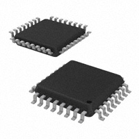
Available in a 32-Pin LQFP Package
Frequency Range From DC to 3.5 GHz
Pin-to-Pin Compatible With MC100 Series
EP111, ES6111, LVEP111, PTN1111
spacer
spacer
DESCRIPTION
The CDCLVP110 clock driver distributes one
differential clock pair of either LVPECL or HSTL
(selectable) input, (CLK0, CLK1) to ten pairs of
differential LVPECL clock (Q0, Q9) outputs with
minimum skew for clock distribution. The
CDCLVP110 can accept two clock sources into an
input multiplexer. The CLK0 input accepts either
LVECL/LVPECL input signals, while CLK1 accepts an
HSTL input signal when operated under LVPECL
conditions. The CDCLVP110 is specifically designed
for driving 50-Ω transmission lines.
The VBB reference voltage output is used if
single-ended input operation is required. In this case
the VBB pin should be connected to CLK0 and
bypassed to GND via a 10-nF capacitor.
However, for high-speed performance up to 3.5 GHz,
the differential mode is strongly recommended.
The CDCLVP110 is characterized for operation from
–40°C to 85°C.
LQFP PACKAGE
(TOP VIEW)
Q3
Q3
Q4
Q4
Q5
Q5
Q6
Q6
spacer
spacer
Table 1. FUNCTION TABLE
24 23 22 21 20 19 18 17
VCC
Q2
Q2
Q1
Q1
Q0
Q0
VCC
25
16
26
15
27
14
28
13
29
12
30
11
31
10
9
32
4
5 6 7
CLK_SEL
ACTIVE CLOCK INPUT
0
CLK0, CLK0
1
CLK1, CLK1
8
VCC
CLK_SEL
CLK0
CLK0
VBB
CLK1
CLK1
VEE
1 2 3
VCC
Q7
Q7
Q8
Q8
Q9
Q9
VCC
1
Please be aware that an important notice concerning availability, standard warranty, and use in critical applications of Texas
Instruments semiconductor products and disclaimers thereto appears at the end of this data sheet.
PRODUCTION DATA information is current as of publication date.
Products conform to specifications per the terms of the Texas
Instruments standard warranty. Production processing does not
necessarily include testing of all parameters.
Copyright © 2002–2011, Texas Instruments Incorporated
�CDCLVP110
SCAS683D – JUNE 2002 – REVISED JANUARY 2011
www.ti.com
These devices have limited built-in ESD protection. The leads should be shorted together or the device placed in conductive foam
during storage or handling to prevent electrostatic damage to the MOS gates.
31
30
29
28
27
26
24
23
3
CLK0
4
CLK0
0
22
21
6
CLK1
7
CLK1
20
1
19
18
17
2
CLK_SEL
15
14
13
12
11
VBB
5
10
Q0
Q0
Q1
Q1
Q2
Q2
Q3
Q3
Q4
Q4
Q5
Q5
Q6
Q6
Q7
Q7
Q8
Q8
Q9
Q9
TERMINAL FUNCTIONS
TERMINAL
NAME
CLK_SEL
DESCRIPTION
NO.
2
Clock select. Used to select between CLK0 and CLK1 input pairs.
CLK0, CLK0
3, 4
Differential LVECL/LVPECL input pair
CLK1, CLK1
6, 7
Differential HSTL input pair
Q [9:0]
11, 13, 15, 18,
20, 22, 24, 27,
29, 31
LVECL/LVPECL clock outputs, these outputs provide low-skew copies of CLKn.
Q[9:0]
10, 12, 14, 17,
19, 21,23, 26,
28, 30
LVECL/LVPECL complementary clock outputs, these outputs provide copies of CLKn.
VBB
5
VCC
1, 9, 16, 25, 32
VEE
8
2
Reference voltage output for single-ended input operation
Supply voltage
Device ground or negative supply voltage in ECL mode
Submit Documentation Feedback
Copyright © 2002–2011, Texas Instruments Incorporated
Product Folder Link(s) :CDCLVP110
�CDCLVP110
www.ti.com
SCAS683D – JUNE 2002 – REVISED JANUARY 2011
ABSOLUTE MAXIMUM RATINGS (1)
VALUE
UNIT
–0.3 to 4.6
V
Input voltage
–0.3 to VCC + 0.5
V
VO
Output voltage
–0.3 to VCC + 0.5
V
IIN
Input current
±20
mA
VEE
Negative supply voltage
IBB
Sink/source current
IO
DC output current
Tstg
Storage temperature range
VCC
Supply voltage
VI
(1)
–0.3 to 4.6
V
–1 to 1
mA
–50
mA
–65 to 150
°C
Stresses beyond those listed under "absolute maximum ratings” may cause permanent damage to the device. These are stress ratings
only, and functional operation of the device at these or any other conditions beyond those indicated under "recommended operating
conditions” is not implied. Exposure to absolute-maximum-rated conditions for extended periods may affect device reliability.
RECOMMENDED OPERATING CONDITIONS
MIN
VCC
TA
Supply voltage (relative to VEE)
(1)
(1)
Operating free-air temperature
NOM
MAX
2.375 2.5/3.3
3.8
V
85
°C
–40
UNIT
Operating junction temperature affects device lifetime. The continuous operation junction temperature is recommended to be at max
110°C. The device ac and dc parameters are specified up to 85°C ambient temperature. See the PCB Layout Guidelines for
CDCLVP110 application note, literature number SCAA057 for more details.
PACKAGE THERMAL IMPEDANCE
TEST CONDITIONS
Thermal resistance junction to ambient (1)
ΘJA
ΘJC
(1)
MAX
UNIT
0 LFM
MIN
74
°C/W
150 LFM
66
°C/W
250 LFM
64
°C/W
500 LFM
61
°C/W
39
°C/W
Thermal resistance junction to case
According to JESD 51-7 standard.
LVECL DC ELECTRICAL CHARACTERISTICS
Vsupply: VCC = 0 V, VEE = -2.375 V to -3.8 V
PARAMETER
IEE
Supply internal current
Output and internal supply
current
ICC
IIN
TEST CONDITIONS
MIN
Absolute value of current
All outputs terminated 50 Ω to VCC – 2 V
Input current
TYP
MAX
–40°C
40
78
25°C
45
82
85°C
48
85
–40°C
343
25°C
370
85°C
380
–40°C, 25°C, 85°C
150
For VEE = –3 to -3.8 V, IBB = -0.2 mA
–40°C, 25°C, 85°C
–1.45
–1.3
–1.15
VEE = –2.375 to –2.75 V, IBB = –0.2 mA
–40°C, 25°C, 85°C
–1.4
–1.25
–1.1
UNIT
mA
mA
µA
VBB
Internally generated bias voltage
VIH
High-level input voltage (CLK_SEL)
–40°C, 25°C, 85°C
–1.165
–0.88
V
VIL
Low-level input voltage (CLK_SEL)
–40°C, 25°C, 85°C
–1.81
–1.475
V
VINPP
Input amplitude (CLK0, CLK0)
–40°C, 25°C, 85°C
0.5
1.3
V
VCM
Common-mode voltage (CLK0,
CLK0)
Cross point of input 9 average (VIH, VIL)
–40°C, 25°C, 85°C
VEE
+ 0.975
–0.3
V
–40°C
–1.26
–0.9
VOH
High-level output voltage
IOH = –21 mA
25°C
–1.2
–0.9
85°C
–1.15
–0.9
(1)
Difference of input 9 VIH–VIL , See Note
(1)
V
V
VINPP minimum and maximum is required to maintain ac specifications, actual device function tolerates a minimum VINPP of 100 mV.
Submit Documentation Feedback
Copyright © 2002–2011, Texas Instruments Incorporated
Product Folder Link(s) :CDCLVP110
3
�CDCLVP110
SCAS683D – JUNE 2002 – REVISED JANUARY 2011
www.ti.com
LVECL DC ELECTRICAL CHARACTERISTICS (continued)
Vsupply: VCC = 0 V, VEE = -2.375 V to -3.8 V
PARAMETER
VOL
TEST CONDITIONS
Low-level output voltage
VOD
MIN
IOL = –5 mA
Differential output voltage swing
Terminated with 50 Ω to VCC – 2 V, See
Figure 3
TYP
MAX
–40°C
–1.85
–1.5
25°C
–1.85
–1.45
85°C
–1.85
–1.4
–40°C, 25°C, 85°C
600
UNIT
V
V
LVPECL/HSTL DC ELECTRICAL CHARACTERISTICS
Vsupply: VCC = 2.375 V to 3.8 V, VEE= 0 V
PARAMETER
IEE
Supply internal current
ICC
Output and internal supply
current
IIN
Input current
VBB
Internally generated bias
voltage
VIH
TEST CONDITIONS
Absolute value of current
All outputs terminated 50 Ω to VCC – 2 V
MIN
TYP
MAX
–40°C
40
78
25°C
45
82
85C
48
85
–40°C
343
25°C
370
85°C
380
–40°C, 25°C, 85°C
150
UNIT
mA
mA
µA
VEE = –3 to –3.8 V, IBB= –0.2 mA
–40°C, 25°C, 85°C
VCC – 1.45
VCC – 1.3
VCC – 1.15
VEE = –2.375 to –2.75 V, IBB = -0.2 mA
–40°C, 25°C, 85°C
VCC– 1.4
VCC – 1.25
VCC – 1.1
High-level input voltage
(CLK_SEL)
–40°C, 25°C, 85°C
VCC - 1.165
VCC – 0.88
V
VIL
Low-level input voltage
(CLK_SEL)
–40°C, 25°C, 85°C
VCC - 1.81
VCC – 1.475
V
VINPP
Input amplitude (CLK0,
CLK0)
Difference of input 9 VIH–VIL, see Note
–40°C, 25°C, 85°C
0.5
1.3
V
VIC
Common-mode
voltage (CLK0, CLK0)
Cross point of input 9 average (VIH, VIL)
–40°C, 25°C, 85°C
0.975
VCC – 0.3
V
VID
Differential input
voltage (CLK1, CLK1)
Difference of input VIH–VIL, See Note
(1)
–40°C, 25°C, 85°C
0.4
1.9
V
VI(x)
Input crossover
voltage (CLK1, CLK1)
Cross point of input 9 average (VIH, VIL)
–40°C, 25°C, 85°C
0.68
0.9
V
–40°C
VCC – 1.26
VCC – 0.9
VOH
High-level output
voltage
IOH = –21 mA
25°C
VCC – 1.2
VCC – 0.9
85°C
VCC - 1.15
VCC - 0.9
-40°C
VCC - 1.85
VCC - 1.5
25°C
VCC - 1.85
VCC - 1.45
85°C
VCC - 1.85
VCC - 1.4
VOL
VOD
(1)
4
Low-level output
voltage
Differential output
voltage swing
(1)
IOL = –5 mA
Terminated with 50 Ω to VCC – 2 V, See
Figure 4
-40°C, 25°C, 85°C
600
V
V
V
mV
VINPP minimum and maximum is required to maintain ac specifications, actual device function tolerates a minimum VINPP of 100 mV.
Submit Documentation Feedback
Copyright © 2002–2011, Texas Instruments Incorporated
Product Folder Link(s) :CDCLVP110
�CDCLVP110
www.ti.com
SCAS683D – JUNE 2002 – REVISED JANUARY 2011
AC ELECTRICAL CHARACTERISTICS
Vsupply: VCC = 2.375 V to 3.8 V, VEE = 0 V or LVECL/LVPECL input VCC = 0 V, VEE = -2.375 V to -3.8 V
PARAMETER
TEST CONDITIONS
tpd
Differential propagation delay CLK0,
CLK0 to all Q0, Q0… Q9, Q9
Input condition: VCM = 1 V,
VPP = 0.5 V
–40°C, 25°C, 85°C
tsk(pp)
Part-to-part skew
See Note B and Figure 1
–40°C, 25°C, 85°C
tsk(o)
Output-to-output skew
See Note A and Figure 1
–40°C, 25°C, 85°C
t(JITTER)
Cycle-to-cycle RMS jitter
f(max)
Maximum frequency
tr/tf
Output rise and fall time (20%, 80%)
MIN
TYP MAX UNIT
230
350
15
–40°C, 25°C, 85°C
Functional up to 3.5 GHz, timing
specifications apply at 1 GHz,
see Figure 3
ps
70
ps
30
ps


 工商网监
湘ICP备2023018690号
工商网监
湘ICP备2023018690号
