User's Guide
SCAU027B – March 2009 – Revised March 2011
Low Phase Noise Clock Evaluation Module
1
2
3
4
5
6
7
8
1
•
•
•
•
•
•
•
Contents
Features ......................................................................................................................
General Description .........................................................................................................
Signal Path and Control Circuitry .........................................................................................
Getting Started ..............................................................................................................
Input Clock Selection .......................................................................................................
Operating Mode Selection .................................................................................................
Output Buffer Termination .................................................................................................
Schematic ....................................................................................................................
1
2
2
2
2
3
5
7
Features
Easy-to-use evaluation module to generate low
phase noise clocks
Easy device setup
Rapid configuration
Control pins configurable through jumpers
Requires 3.3-V power supply
Single-ended or crystal input clock reference
Termination available for LVPECL, LVDS, and
LVCMOS output clocks
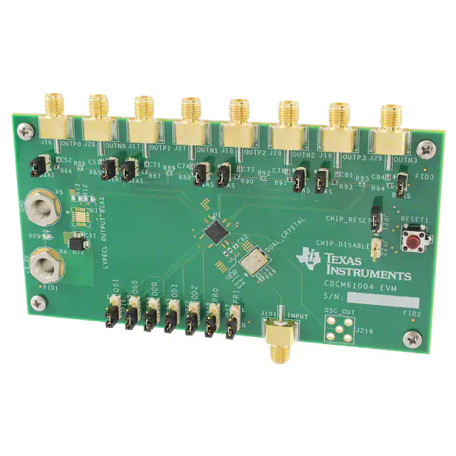
Figure 1. CDCM6100xEVM Evaluation Board
All trademarks are the property of their respective owners.
SCAU027B – March 2009 – Revised March 2011
Submit Documentation Feedback
Low Phase Noise Clock Evaluation Module
© 2009–2011, Texas Instruments Incorporated
1
�General Description
2
www.ti.com
General Description
The CDCM61001, CDCM61002, and CDCM61004 are high-performance, low phase noise clock
generators. Each device has one crystal/low-voltage CMOS (LVCMOS) input buffer and one, two, or four
universal outputs depending on the respective device.
This is a programmable clock generator with control pins only. No EEPROM or programming interface is
necessary to program these devices.
The CDCM6100x evaluation module (EVM) is designed to demonstrate the electrical performance of the
CDCM61004 and is representative of the performance of the CDCM61001 and CDCM61002. This
fully-assembled and factory-tested evaluation board allows complete validation of all device functions.
For optimum performance, the board is equipped with 50-Ω SMA connectors and well-controlled, 50-Ω
impedance microstrip transmission lines.
Throughout this document, the abbreviation EVM and the phrases evaluation module and evaluation
board are synonymous with the CDCM6100xEVM. For clarity of reading, the abbreviation CDCM6100x
refers to the CDCM61001, CDCM61002, and CDCM61004, unless otherwise noted.
2.1
Reference Documents
The related documents listed in Table 1 are available through the Texas Instruments web site at
www.ti.com.
Table 1. EVM-Compatible Device Data Sheets
3
Device
Data Sheet
CDCM61001
SCAS869
CDCM61002
SCAS870
CDCM61004
SCAS871
Signal Path and Control Circuitry
The CDCM6100x supports either a crystal input or a single-ended clock with a frequency range of 21.875
MHz to 28.47 MHz. The internal VCO operates from 1.75 GHz to 2.05 GHz. The output buffers provide
output frequencies from 43.75 MHz to 683.264 MHz for low-voltage differential signaling (LVDS) and
low-voltage positive emitter coupled logic (LVPECL), and from 43.75 MHz to 250 MHz for LVCMOS. An
optional, bypassed LVCMOS output is also available.
The output frequency depends on the input frequency, Prescaler, Feedback, and Output Divider settings.
See the respective product data sheet (listed in Table 1) for complete descriptions of the various settings.
4
Getting Started
The EVM has self-explanatory labeling. Additionally, the naming conventions used for the EVM
correspond to that used in the respective product data sheets. Words shown in bold italics in this
document show the same name and label on the EVM board itself. The EVM can be used with either a
crystal input or external, single-ended clock input.
4.1
Power-Supply Connection
Connect the power-supply source to the banana plug labeled 3.3V (P4) and connect the ground of the
power-supply source to GND (P5). There are decoupling capacitors and ferrite bead to isolate the device
power pins dedicated for the PLL from the other power pins.
This EVM can operate from a 3.0-V to 3.6-V supply voltage.
5
Input Clock Selection
The CDCM6100xEVM offers the options to use either a crystal or a single-ended clock source as the clock
input.
2
Low Phase Noise Clock Evaluation Module
© 2009–2011, Texas Instruments Incorporated
SCAU027B – March 2009 – Revised March 2011
Submit Documentation Feedback
�Operating Mode Selection
www.ti.com
5.1
Configuring a Crystal Input
The EVM is available with an optional 25-MHz crystal. The EVM offers a dual footprint for a 6-pin (5 mm ×
7 mm) and 4-pin (3 mm x 5 mm) crystal. For a parallel load resonant crystal, the configuration should be
similar to that shown in Figure 2.
XIN
CDCM6100x
Note: This configuration assumes that the crystal is placed very closed to the XIN pin on the device.
Figure 2. CDCM6100xEVM Configuration with Parallel Load Resonant Crystal Clock Source
5.2
Configuring a Single-Ended Input
For a single-ended clock, remove the crystal if the board already has a crystal installed. Use SMA
connector J101 for a single-ended input clock. Place a 50-Ωresistor in R69 if the clock is provided from a
signal generator and if the signal generator requires a 50-Ω load for its operation. If the input clock is
provided from another board or the LVCMOS buffer, do not place any resistor here.
Capacitor C61 (100 nF) is required for ac coupling, as shown in Figure 3.
C61
100 nF
J101
R69
50 W
(Optional)
CDCM6100x
Figure 3. Single-Ended Connection Configuration
6
Operating Mode Selection
The CDCM6100x is a PLL-based device and offers several modes of operation. Selection of the available
control pins provides a set of output frequencies with different signaling levels. See the respective product
data sheets for detailed device configuration information.
6.1
Prescaler Divider and Feedback Divider Settings
JP17 (PR1) and JP18 (PR0) are the control pin jumpers for Prescalar Divider and Feedback Divider
selection, respectively. Use these jumpers only for logic '0'. These pins have internal 150-kΩ pull-up
resistors; it is recommended to use the internal pull-up resistor only for logic '1'.
Table 2 summarizes the available prescaler divider and feedback divider values with the corresponding
PFD frequency range.
SCAU027B – March 2009 – Revised March 2011
Submit Documentation Feedback
Low Phase Noise Clock Evaluation Module
© 2009–2011, Texas Instruments Incorporated
3
�Operating Mode Selection
www.ti.com
Table 2. Available Prescaler Divider and Feedback Divider Values with PFD
Frequency Range
Control Inputs
(1)
Feedback
Divider
PFD Frequency
(1)
PR1
PR0
Prescaler
Divider
Minimum
Maximum
0
0
3
24
24.305
28.47
0
1
5.
15
23.33
27.33
1
0
3
25
23.33
27.33
1
1
4
20
21.875
25.62
PFD frequency = Reference Clock Frequency
The product of the prescaler divider and the feedback divider with reference clock frequency provides the
frequency at which the VCO operates:
VCO Frequency = Prescaler Divider × Feedback Divider × Reference Clock Frequency
6.2
Output Divider Selections
JP14 (OD0), JP13 (OD1), and JP12 (OD2) are the jumpers for the output dividers. Depending on whether
the device operates in logic '1' or logic '0', the divider offers up to six different frequencies. All outputs
have the same frequency because the outputs are generated from the same divider.
Table 3 lists the available output divider values.
Table 3. Programmable Output Divider Values
Control Inputs
OD2
OD1
OD0
Output Divider
0
0
0
1
0
0
1
2
0
1
0
3
0
1
1
4
1
0
1
6
1
1
1
8
Output Frequency = VCO Frequency / (Prescaler Divider × Output Divider)
6.3
Output Buffer Type Selection
JP16 (OS1) and JP15 (OS0) are the jumpers for output buffer selection (LVCMOS, LVDS, or LVPECL).
Each output pair provides two in-phase LVCMOS clocks.
Table 4 shows the output buffer options.
Table 4. Output Buffer Options
Control Inputs
4
OS1
OS0
Output Type
0
0
LVCMOS, OSC_OUT Off
0
1
LVDS, OSC_OUT Off
1
0
LVPECL, OSC_OUT Off
1
1
LVPECL, OSC_OUT On
Low Phase Noise Clock Evaluation Module
© 2009–2011, Texas Instruments Incorporated
SCAU027B – March 2009 – Revised March 2011
Submit Documentation Feedback
�Output Buffer Termination
www.ti.com
NOTE: A bypassed output (same as the reference clock frequency) is only available with LVPECL
outputs.
6.4
Using ENABLE and RSTN Pins
JP22 (CHIP-DISABLE) is the jumper for the CE pin. This pin has an internal, 150-kΩ, pull-up resistor; it is
recommended to use the internal pull-up resistor only for logic '1'.
Table 5 summarizes the power-down configuration.
Table 5. Power-Down Configuration
Control Input
CE
Operating Condition
Output
0
Power Down
Hi-Z
1
Normal
Active
Do not connect this jumper for normal operation.
The RSTN pin is connected to both CHIP_RESET jumper JP21 and pushbutton switch RESET1. Either
option can be used to reset the device (including recalibrating the PLL). If any settings change on either
the PR0 or the PR1 pins, PLL recalibration is required to generate the proper VCO frequency.
Table 6 lists the RESET configuration options.
Table 6. Reset Configuration
Control Input
RSTN
7
Operating Condition
Output
Hi-Z
0
Device Reset
0→1
PLL Recalibration
Hi-Z
1
Normal
Active
Output Buffer Termination
This EVM is designed to support proper termination for all three types of output buffers. Proper
components must be selected or placed to make sure the chosen output buffer works properly with the
correct termination as expected. Figure 4 shows different ways to terminate the outputs of the device.
Figure 4. EVM Output Termination Options
7.1
Output Buffer Examples
LVPECLOutput Buffer: Jumpers J24 and J26 should be used. This connection is illustrated in Figure 5.
SCAU027B – March 2009 – Revised March 2011
Submit Documentation Feedback
Low Phase Noise Clock Evaluation Module
© 2009–2011, Texas Instruments Incorporated
5
�Output Buffer Termination
www.ti.com
R84
150 W
JP24
C52
100 nF
J16
OUTP0
CDCM6100x
C57
100 nF
J26
OUTN0
R845
150 W
JP26
Figure 5. LVPECL Output Setup
LVDS Output Buffer: Remove jumpers J24 and J26. A 100-Ω resistor can be placed at the R85
placeholder, if necessary. If the output pair is connected to an oscilloscope through 50-Ω SMA cables,
then the oscilloscope 50-Ω to ground connection should take care of this termination, and the 100-Ω
resistor is no longer necessary. Figure 6 illustrates this output buffer configuration.
R84
150 W
JP24
C52
100 nF
J16
OUTP0
CDCM6100x
R86
100 W
(Optional)
C57
100 nF
J26
OUTN0
R845
150 W
JP26
Figure 6. LVDS Output Setup
LVCMOS Output Buffer: This LVCMOS buffer typically has 30 Ω internal impedance. An external 22-Ω
series resistor is recommended for a 50-Ω impedance characteristic line. For an SMA connection to an
oscilloscope, the output can be connected as ac-coupled (using C52 and C58). A lower-than-expected
swing will be observed because the LVCMOS driver is not capable of driving a 50 Ω to ground load.
Figure 5 describes this connection interface.
7.2
Availability of Optional Output
An optional bypassed output (OSC_OUT) is only available if the PLL output(s) are chosen at an LVPECL
signaling level. J219 is the SMA placeholder for this output.
6
Low Phase Noise Clock Evaluation Module
© 2009–2011, Texas Instruments Incorporated
SCAU027B – March 2009 – Revised March 2011
Submit Documentation Feedback
�Schematic
www.ti.com
8
Schematic
Figure 7. CDCM6100xEVM Schematic
SCAU027B – March 2009 – Revised March 2011
Submit Documentation Feedback
Low Phase Noise Clock Evaluation Module
© 2009–2011, Texas Instruments Incorporated
7
�EVALUATION BOARD/KIT IMPORTANT NOTICE
Texas Instruments (TI) provides the enclosed product(s) under the following conditions:
This evaluation board/kit is intended for use for ENGINEERING DEVELOPMENT, DEMONSTRATION, OR EVALUATION PURPOSES
ONLY and is not considered by TI to be a finished end-product fit for general consumer use. Persons handling the product(s) must have
electronics training and observe good engineering practice standards. As such, the goods being provided are not intended to be complete
in terms of required design-, marketing-, and/or manufacturing-related protective considerations, including product safety and environmental
measures typically found in end products that incorporate such semiconductor components or circuit boards. This evaluation board/kit does
not fall within the scope of the European Union directives regarding electromagnetic compatibility, restricted substances (RoHS), recycling
(WEEE), FCC, CE or UL, and therefore may not meet the technical requirements of these directives or other related directives.
Should this evaluation board/kit not meet the specifications indicated in the User’s Guide, the board/kit may be returned within 30 days from
the date of delivery for a full refund. THE FOREGOING WARRANTY IS THE EXCLUSIVE WARRANTY MADE BY SELLER TO BUYER
AND IS IN LIEU OF ALL OTHER WARRANTIES, EXPRESSED, IMPLIED, OR STATUTORY, INCLUDING ANY WARRANTY OF
MERCHANTABILITY OR FITNESS FOR ANY PARTICULAR PURPOSE.
The user assumes all responsibility and liability for proper and safe handling of the goods. Further, the user indemnifies TI from all claims
arising from the handling or use of the goods. Due to the open construction of the product, it is the user’s responsibility to take any and all
appropriate precautions with regard to electrostatic discharge.
EXCEPT TO THE EXTENT OF THE INDEMNITY SET FORTH ABOVE, NEITHER PARTY SHALL BE LIABLE TO THE OTHER FOR ANY
INDIRECT, SPECIAL, INCIDENTAL, OR CONSEQUENTIAL DAMAGES.
TI currently deals with a variety of customers for products, and therefore our arrangement with the user is not exclusive.
TI assumes no liability for applications assistance, customer product design, software performance, or infringement of patents or
services described herein.
Please read the User’s Guide and, specifically, the Warnings and Restrictions notice in the User’s Guide prior to handling the product. This
notice contains important safety information about temperatures and voltages. For additional information on TI’s environmental and/or
safety programs, please contact the TI application engineer or visit www.ti.com/esh.
No license is granted under any patent right or other intellectual property right of TI covering or relating to any machine, process, or
combination in which such TI products or services might be or are used.
FCC Warning
This evaluation board/kit is intended for use for ENGINEERING DEVELOPMENT, DEMONSTRATION, OR EVALUATION PURPOSES
ONLY and is not considered by TI to be a finished end-product fit for general consumer use. It generates, uses, and can radiate radio
frequency energy and has not been tested for compliance with the limits of computing devices pursuant to part 15 of FCC rules, which are
designed to provide reasonable protection against radio frequency interference. Operation of this equipment in other environments may
cause interference with radio communications, in which case the user at his own expense will be required to take whatever measures may
be required to correct this interference.
EVM WARNINGS AND RESTRICTIONS
It is important to operate this EVM within the input voltage range of 3 V to 3.6 V and the output voltage range of 0 V to 3.6 V.
Exceeding the specified input range may cause unexpected operation and/or irreversible damage to the EVM. If there are questions
concerning the input range, please contact a TI field representative prior to connecting the input power.
Applying loads outside of the specified output range may result in unintended operation and/or possible permanent damage to the EVM.
Please consult the EVM User's Guide prior to connecting any load to the EVM output. If there is uncertainty as to the load specification,
please contact a TI field representative.
During normal operation, some circuit components may have case temperatures greater than +120°C. The EVM is designed to operate
properly with certain components above +85°C as long as the input and output ranges are maintained. These components include but are
not limited to linear regulators, switching transistors, pass transistors, and current sense resistors. These types of devices can be identified
using the EVM schematic located in the EVM User's Guide. When placing measurement probes near these devices during operation,
please be aware that these devices may be very warm to the touch.
Mailing Address: Texas Instruments, Post Office Box 655303, Dallas, Texas 75265
Copyright © 2009-2011, Texas Instruments Incorporated
�IMPORTANT NOTICE
Texas Instruments Incorporated and its subsidiaries (TI) reserve the right to make corrections, modifications, enhancements, improvements,
and other changes to its products and services at any time and to discontinue any product or service without notice. Customers should
obtain the latest relevant information before placing orders and should verify that such information is current and complete. All products are
sold subject to TI’s terms and conditions of sale supplied at the time of order acknowledgment.
TI warrants performance of its hardware products to the specifications applicable at the time of sale in accordance with TI’s standard
warranty. Testing and other quality control techniques are used to the extent TI deems necessary to support this warranty. Except where
mandated by government requirements, testing of all parameters of each product is not necessarily performed.
TI assumes no liability for applications assistance or customer product design. Customers are responsible for their products and
applications using TI components. To minimize the risks associated with customer products and applications, customers should provide
adequate design and operating safeguards.
TI does not warrant or represent that any license, either express or implied, is granted under any TI patent right, copyright, mask work right,
or other TI intellectual property right relating to any combination, machine, or process in which TI products or services are used. Information
published by TI regarding third-party products or services does not constitute a license from TI to use such products or services or a
warranty or endorsement thereof. Use of such information may require a license from a third party under the patents or other intellectual
property of the third party, or a license from TI under the patents or other intellectual property of TI.
Reproduction of TI information in TI data books or data sheets is permissible only if reproduction is without alteration and is accompanied
by all associated warranties, conditions, limitations, and notices. Reproduction of this information with alteration is an unfair and deceptive
business practice. TI is not responsible or liable for such altered documentation. Information of third parties may be subject to additional
restrictions.
Resale of TI products or services with statements different from or beyond the parameters stated by TI for that product or service voids all
express and any implied warranties for the associated TI product or service and is an unfair and deceptive business practice. TI is not
responsible or liable for any such statements.
TI products are not authorized for use in safety-critical applications (such as life support) where a failure of the TI product would reasonably
be expected to cause severe personal injury or death, unless officers of the parties have executed an agreement specifically governing
such use. Buyers represent that they have all necessary expertise in the safety and regulatory ramifications of their applications, and
acknowledge and agree that they are solely responsible for all legal, regulatory and safety-related requirements concerning their products
and any use of TI products in such safety-critical applications, notwithstanding any applications-related information or support that may be
provided by TI. Further, Buyers must fully indemnify TI and its representatives against any damages arising out of the use of TI products in
such safety-critical applications.
TI products are neither designed nor intended for use in military/aerospace applications or environments unless the TI products are
specifically designated by TI as military-grade or "enhanced plastic." Only products designated by TI as military-grade meet military
specifications. Buyers acknowledge and agree that any such use of TI products which TI has not designated as military-grade is solely at
the Buyer's risk, and that they are solely responsible for compliance with all legal and regulatory requirements in connection with such use.
TI products are neither designed nor intended for use in automotive applications or environments unless the specific TI products are
designated by TI as compliant with ISO/TS 16949 requirements. Buyers acknowledge and agree that, if they use any non-designated
products in automotive applications, TI will not be responsible for any failure to meet such requirements.
Following are URLs where you can obtain information on other Texas Instruments products and application solutions:
Products
Applications
Audio
www.ti.com/audio
Communications and Telecom www.ti.com/communications
Amplifiers
amplifier.ti.com
Computers and Peripherals
www.ti.com/computers
Data Converters
dataconverter.ti.com
Consumer Electronics
www.ti.com/consumer-apps
DLP® Products
www.dlp.com
Energy and Lighting
www.ti.com/energy
DSP
dsp.ti.com
Industrial
www.ti.com/industrial
Clocks and Timers
www.ti.com/clocks
Medical
www.ti.com/medical
Interface
interface.ti.com
Security
www.ti.com/security
Logic
logic.ti.com
Space, Avionics and Defense
www.ti.com/space-avionics-defense
Power Mgmt
power.ti.com
Transportation and
Automotive
www.ti.com/automotive
Microcontrollers
microcontroller.ti.com
Video and Imaging
www.ti.com/video
RFID
www.ti-rfid.com
Wireless
www.ti.com/wireless-apps
RF/IF and ZigBee® Solutions
www.ti.com/lprf
TI E2E Community Home Page
e2e.ti.com
Mailing Address: Texas Instruments, Post Office Box 655303, Dallas, Texas 75265
Copyright © 2011, Texas Instruments Incorporated
�