User's Guide
SCAU049A – May 2012 – Revised January 2013
CDCM6208 Evaluation Board
1
2
3
4
5
6
7
8
9
Contents
Features ...................................................................................................................... 2
General Description ......................................................................................................... 3
Signal Path and Control .................................................................................................... 4
Software-Selectable Option ................................................................................................ 4
Installing the EVM Control Software and USB Driver .................................................................. 4
5.1
CDCM6208 Control User Interface .............................................................................. 4
Using the EVM Control Software ......................................................................................... 5
6.1
Primary and Secondary Reference Signal Type Selection ................................................... 5
6.2
Input Divider For Primary Reference ®) Selection ............................................................ 5
6.3
Input MUX Selection ............................................................................................... 6
6.4
Input Divider (M) For the PLL Selection ........................................................................ 6
6.5
Charge Pump Current Selection ................................................................................. 6
6.6
Loop Filter (3rd Pole only) Selection .............................................................................. 6
6.7
Feedback Divider Selection ....................................................................................... 6
6.8
Prescalar Dividers (PS_A and PS_B) Selection ............................................................... 6
6.9
VCO Frequency Selection ........................................................................................ 6
6.10 Output MUX Selection ............................................................................................. 6
6.11 Output Dividers ..................................................................................................... 6
6.12 Output Signal Type Selection .................................................................................... 7
6.13 Additional Features ................................................................................................ 7
Configuring the Board ...................................................................................................... 7
7.1
Selecting the Interface Connection .............................................................................. 7
7.2
Configuring the Power Supply .................................................................................... 7
7.3
Configuring the Reference Inputs ................................................................................ 8
7.4
Configuring the Control Pins ...................................................................................... 9
7.5
Selecting the Loop Filter ......................................................................................... 10
7.6
Configuring the Outputs ......................................................................................... 10
7.7
Using the MSP430 as a Bootloader ............................................................................ 10
A Step by Step Guide on Updating the TUSB3210 Firmware for I2C communication on the CDCM6208
EVM ......................................................................................................................... 11
8.1
Required Software and Hardware .............................................................................. 11
8.2
Installing TI USB EEPROM Burner Software ................................................................. 11
8.3
Programming the CDCM6208 EVM’s TUSB3210 ............................................................ 11
CDCM6208V2 EVM Board Schematic ................................................................................. 14
List of Figures
1
CDCM6208 Evaluation Board ............................................................................................. 3
2
Initial GUI Screen
3
4
5
6
..........................................................................................................
Jumper Configuration For USB Power Supply ..........................................................................
EVM SW4 Location .......................................................................................................
TUSB3210 EEPROM Burner Software .................................................................................
CDCM6208V1/CDCM6208V2 EVM Control Modes ..................................................................
5
8
12
13
14
All trademarks are the property of their respective owners.
SCAU049A – May 2012 – Revised January 2013
Submit Documentation Feedback
Copyright © 2012–2013, Texas Instruments Incorporated
CDCM6208 Evaluation Board
1
�Features
www.ti.com
7
CDCM6208V1/CDCM6208V2 EVM Device Pins and Bypassing ................................................... 15
8
CDCM6208V1/CDCM6208V2 EVM Reference Inputs
9
CDCM6208V1/CDCM6208V2 EVM Outputs 0 to 3 ................................................................... 17
10
CDCM6208V1/CDCM6208V2 EVM Outputs 4 to 7 ................................................................... 18
11
CDCM6208V1/CDCM6208V2 EVM Power Supplies ................................................................. 19
12
Onboard MSP430G2001
...............................................................
................................................................................................
16
20
List of Tables
1
Input Selection Jumper Settings .......................................................................................... 9
2
Mode Selection Jumper Settings
3
4
1
.........................................................................................
STATUS1 Functional Description .......................................................................................
Device Control Pin Functions ............................................................................................
9
10
10
Features
•
•
•
•
•
Easy-to-use evaluation module generating low-phase noise clocks up to 800 MHz
Easy device programming via host-powered USB port or control pins
Rapid configuration with provided EVM Control Software
Powered from the USB port, or by an external 3.3-, 2.5-, or 1.8-V power supply
Single-ended or differential input; external crystal for use with on-chip oscillator
Words shown in bold italics in this document show the same name and label on the EVM board itself.
2
CDCM6208 Evaluation Board
SCAU049A – May 2012 – Revised January 2013
Submit Documentation Feedback
Copyright © 2012–2013, Texas Instruments Incorporated
�General Description
www.ti.com
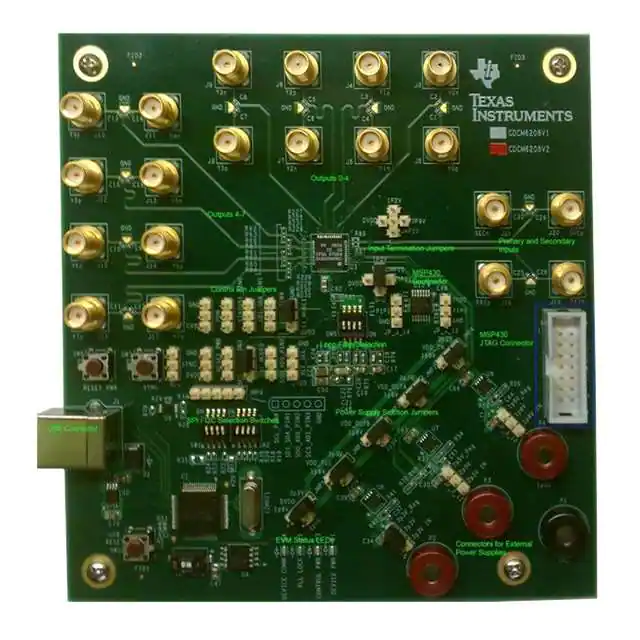
Figure 1. CDCM6208 Evaluation Board
2
General Description
The CDCM6208 is a highly-versatile, low-jitter, low-power frequency synthesizer generating up to eight
clock outputs, selectable between LVPECL-like high-swing CML, normal-swing CML, LVDS-like low-power
CML, HCSL, or LVCMOS, from one of two inputs that can feature a low frequency crystal or CML,
LVPECL, LVDS, or LVCMOS signals. It also features an innovative fractional divider architecture for four
of its outputs generating any frequency with better than 1 ppm frequency accuracy. The device is easily
configured through I2C or SPI programming interfaces. In the absence of serial interface, pin-programming
mode is available and can set the device in many distinct preprogrammed configurations using control
pins. Two versions are available, (CDCM62008V1 and CDCM6208V2) depending on the VCO frequency
ranges.
The CDCM6208 is programmed through an SPI or I2C interface using the supplied EVM programming
graphical user interface (GUI).
SCAU049A – May 2012 – Revised January 2013
Submit Documentation Feedback
Copyright © 2012–2013, Texas Instruments Incorporated
CDCM6208 Evaluation Board
3
�Signal Path and Control
www.ti.com
The CDCM6208 evaluation module (EVM) demonstrates the electrical performance of the device. This
fully-assembled, factory-tested evaluation board allows complete validation of all device functions. For
optimum performance, the board is equipped with 50-Ω SMA connectors and well-controlled 50-Ω
impedance micro strip transmission lines.
3
Signal Path and Control
The CDCM6208 provides two selectable inputs – PRI_REF and SEC_REF. The PRI_REF and SEC_REF
accept either differential- (CML, LVDS) or single-ended LVCMOS signals, up to 250 MHz. Besides the
external clocks, SEC_REF allows the use of an external crystal in the frequency range of 10 MHz to 50
MHz. The EVM provides a PC-board footprint for mounting a 3.2 mm × 2.5 mm SMD crystal. If the
SEC_REF is driven through the SMA connector, the on-board crystal and R72 and R73 must be removed
and R87 must be populated with a 0-Ω resistor (R89 must also be populated with a 0-Ω resistor for a
differential input signal). The device does not have any internal termination or biasing, therefore, proper
biasing and termination options are available on the EVM, if needed.
The CDCM6208 provides up to eight differential signals. Out of eight outputs, four differential outputs can
convert into eight singled LVCMOS signals. A maximum of eight differential or 4 differential and eight
singled LVCMOS clocks or any of the various combinations are possible.
The device operates as a jitter cleaner or as a frequency synthesizer. The CDCM6208 requires a partiallyexternal loop filter. The EVM provides four loop filter options – two filters are for synthesizer mode and the
other two for jitter-cleaning mode. The loop-filter selection affects the phase noise and loop stability of the
PLL.
In pin mode, the device option is selected by five control pins. In programming mode, options are selected
by programming the on-chip registers. The CDCM6208 data sheet provides the detailed information
needed for configuration and use of this device.
Four outputs (Y0-Y3) are configurable as an LVDS, CML, or LVPECL and another four outputs (Y4-Y7)
are configurable as LVDS, HCSL, or LVCMOS. All outputs are connected to SMA with AC coupling. Y4-Y7
outputs provide the options of 50 Ω to ground (for HCSL outputs).
The LVCMOS outputs can operate at frequencies up to 200 MHz. The HS-CML and NS-CML outputs
operate at up to 800 MHz. The LP-CML and HCSL outputs operate at up to 400 MHz.
4
Software-Selectable Option
The EVM control software communicates with the CDCM6208 through a USB interface and the
CDCM6208 SPI or I2C port. The USB controller is normally powered over the USB cable. When the
USB/SPI or USB/I2C programming interface is available for use, the on-board LED, D3, is illuminated.
The CDCM6208 GUI can save device configurations into a configuration file (.INI), which are loaded at a
later time restoring the saved settings.
5
Installing the EVM Control Software and USB Driver
Start the EVM software installation by double-clicking on the file named CDCM6208_Installer.exe. The
Microsoft .NET Framework 4.0 is automatically downloaded and installed on the computer, if it is not
already installed. The installer attempts installation of the EVM hardware driver.
5.1
CDCM6208 Control User Interface
The following represents the initial screen of the GUI:
4
CDCM6208 Evaluation Board
SCAU049A – May 2012 – Revised January 2013
Submit Documentation Feedback
Copyright © 2012–2013, Texas Instruments Incorporated
�Using the EVM Control Software
www.ti.com
Figure 2. Initial GUI Screen
6
Using the EVM Control Software
The graphical layout of the programming software is based on the functional structure of the CDCM6208.
The following settings are changed with this tool:
•
•
•
•
•
•
•
•
•
•
Input frequency
Input divider
Input type
Input selection to the PLL
Charge-pump current
Internal loop filter components (3rd Pole)
Pre-scalar and feedback divider
Output MUX selection
Output divider or frequency
Output type
This software also sets input and output buffer supply voltage bits (1.8 V or 2.5/3.3 V)..
6.1
Primary and Secondary Reference Signal Type Selection
Using the pull-down menu, input clock type is selected or input buffer is disabled. The input signal type for
Primary clock and Secondary clock are set to either LVDS, CML, or LVCMOS. Additionally, crystal input is
selectable for Secondary input.
6.2
Input Divider For Primary Reference ®) Selection
The primary reference has a 4-bit divider ®), therefore, up to 16 appropriate divider values are available.
SCAU049A – May 2012 – Revised January 2013
Submit Documentation Feedback
Copyright © 2012–2013, Texas Instruments Incorporated
CDCM6208 Evaluation Board
5
�Using the EVM Control Software
6.3
www.ti.com
Input MUX Selection
The CDCM6208 employs a smart MUX selecting the input clock for the PLL. The input clock is either
primary reference only, secondary reference only, or in automatic selection mode. Toggling the connection
line, the proper reference input is selected. If the Auto box is selected, automatic input selection mode is
activated.
6.4
Input Divider (M) For the PLL Selection
The input (M) divider is a continuous 14-b counter (1–16384) that is present after the Smart Input MUX.
The output of the M divider sets the PFD frequency to the PLL and must be in the range of 8 kHz to 100
MHz.
6.5
Charge Pump Current Selection
The charge-pump current value is chosen from the pull-down menu. The allowable range of the chargepump current is from 500 µA to 4 mA.
6.6
Loop Filter (3rd Pole only) Selection
C1, R2, and C2 are external loop filter components connected to the ELF pin, but the 3rd pole of the loop
filter is internal to the device with R3 and C3 register-selectable. Appropriate C3 and R3 values are
selected using the pull-down menu.
6.7
Feedback Divider Selection
The feedback divider (N) is made up of a cascaded 8-b counter divider (1–256) and a 10-b counter divider
(1–1024) present on the feedback path of the PLL. If the divider value is available, the software
automatically selects the proper combination from the two cascaded dividers. The output of the N divider
sets the PFD frequency to the PLL and must be in the range of 8 kHz to 100 MHz.
6.8
Prescalar Dividers (PS_A and PS_B) Selection
The prescaler (PS) dividers are fed by the output of the VCO and are distributed to the output dividers
(PS_A to the dividers for outputs Y0, Y1, Y4, and Y5. PS_B to the dividers for outputs Y2, Y3, Y6, and
Y7). PS_A also completes the PLL, driving the input of the feedback divider (N). Appropriate values are
set for each prescalar using the pull-down menu.
6.9
VCO Frequency Selection
The VCO frequency value depends on the selection of reference input frequency and input dividers,
prescalar (PS_A), and feedback dividers. The software automatically calculates the VCO frequency, based
on the selection, and provides the value. If the calculated VCO frequency is outside of the range, it flashs
red.
6.10 Output MUX Selection
Both Y4 and Y5 outputs have multiplexers which select one of the three inputs (PRI_REF, SEC_REF, or
PS_A) for the outputs. The proper input is selected for the outputs by dragging the connection line.
6.11 Output Dividers
Outputs Y0 and Y1 share one 8-bit continuous integer divider and outputs Y2 and Y3 share another 8-bit
continuous integer divider; therefore, these pairs of outputs have the same frequency. Each of the outputs
Y4, Y5, Y6, and Y7 have 8-bit continuous integer dividers and in addition, 20-bit fractional dividers. The
software automatically chooses the right divider values for Y4–Y7 outputs from the integer and fractional
dividers, if the expected output frequency in the desired output box is provided.
6
CDCM6208 Evaluation Board
SCAU049A – May 2012 – Revised January 2013
Submit Documentation Feedback
Copyright © 2012–2013, Texas Instruments Incorporated
�Configuring the Board
www.ti.com
6.12 Output Signal Type Selection
Outputs Y0–Y3 offer LP-CML (LVDS like), CML or HS-CML (LVPECL like) signaling types. Using the pulldown menu, one of the signal types is selected for each output or can disable the output channel
completely. Outputs Y4–Y7 offer LP-CML (LVDS like), HCSL or LVCMOS signaling types. Using the pulldown menu, one of the signal types is selected for each output or can disable the output channel
completely. If the LVCMOS signal type is selected, check Enable boxes, enabling the outputs individually.
6.13 Additional Features
The EVM software GUI comes with tools that are helpful in optimizing the device settings for best
performance. These include a Frequency Planning Tool, the Loop Filter Simulator, and the Phase-Noise
Simulator. Each of these tools are described in detail in the Help documentation provided in the GUI.
7
Configuring the Board
The CDCM6208 is a programmable clock driver with many options. The EVM was designed with
maximum flexibility so engineers can configure the EVM for operation at its desired mode.
7.1
Selecting the Interface Connection
The CDCM6208 is configurable via the serial interface or control pins. Both SPI and I2C interface options
are available for configuring the device. Switch SW1 is dedicated for the SPI interface and switch SW2 is
for the I2C interface. The selected interface switch must be turned on and the other switch must be turned
off. Both switches must be turned off for Pin control mode.
Header JMP9 also connects an external host to SPI or I2C.
7.2
Configuring the Power Supply
The device is powered up with an external power supply or on-board regulators powered by an attached
USB cable. The EVM has options for 1.8-, 2.5-, and 3.3-V power supplies. These supply voltages are
external to, or internal from the regulators. It has five different rails – two for outputs, one for PLL, one for
digital logic, and one for reference input power supplies.
The banana jacks (P2, P3, and P4) are external 3.3 V, 2.5 V, and 1.8 V, respectively. Banana jack P1 is
for GND. Low-dropout regulators U6, U7, and U8, generate 3.3 V, 2.5 V, and 1.8 V, respectively. The
jumper on header JP_3_10 selects between an external or internal 3.3 V, the jumper on header JP_3_11
selects between an external or internal 2.5 V, and the jumper on header JP_3_12 selects between an
external or internal 1.8 V.
The jumpers on the header JMP5 select for the DVDD power rail, JMP1 selects for the PLL power rails,
JMP3 selects for the output power rails (Y2, Y3, Y6, and Y7), JPM2 selects for the output power rails (Y0,
Y1, Y4, and Y5) and JPM4 selects for the reference input power rails from 3.3-, 2.5-, and 1.8-V power
supplies. Mixed power supplies for this device are possible, using these headers.
NOTE: A USB cable must be connected for biasing voltage generation of 1.2 V and 0.9 V for the
reference inputs. These biasing voltages are generated by the on-board regulators which rely
on the USB supply. Figure 3 shows the jumper configuration for a USB power supply. The
EVM settings drive the device from the USB with 1.8-V and 3.3-V supplies. Jumpers for the
header JP_3_10 are set to 3.3-V regulator and for JP_3_3_12 header to 1.8-V regulator.
DVDD (JMP5), VDD_PLL (JMP1), VDD_IN (JMP4), and VDD_OUTB (JMP3) supplies are
set to 1.8 V and VDD_OUTA (JMP2) supply is set to 3.3 V. The entire device is running at
1.8 V, except the Y0, Y1, Y4, and Y5 outputs which are running at 3.3 V.
SCAU049A – May 2012 – Revised January 2013
Submit Documentation Feedback
Copyright © 2012–2013, Texas Instruments Incorporated
CDCM6208 Evaluation Board
7
�Configuring the Board
www.ti.com
Figure 3. Jumper Configuration For USB Power Supply
7.3
Configuring the Reference Inputs
The CDCM62008 offers two inputs (PRI_REF and SEC_REF). SMA J18 and J19 are dedicated for
PRI_REF (IN1p and IN1n) and SMA J20 and J21 are dedicated for SEC_REF (1N2p and 1N2n). Both
inputs in the EVM are AC-coupled, by default, using coupling capacitors (C25 and C26 for PRI_REF and
C29 and C30 for SEC_REF). CDCM6208 does NOT have any internal termination or biasing; so, external
biasing is required after AC coupling. Headers JMP10 and JPM11 provide the options for PRI_REF input
biasing and SEC_REF input biasing, respectively. Depending on the input signaling level and power
supply selection, proper biasing must be selected, see Table 1.
8
CDCM6208 Evaluation Board
SCAU049A – May 2012 – Revised January 2013
Submit Documentation Feedback
Copyright © 2012–2013, Texas Instruments Incorporated
�Configuring the Board
www.ti.com
Table 1. Input Selection Jumper Settings
Input Signaling Level
Input Supply Voltage
JPM10 and JPM11 Selection
CML
1.8 V/2.5 V/3.3 V
DVDD
LVDS
2.5 V/3.3 V
1P2V
LVDS
1.8 V
0P9V
LVCMOS
1.8 V/2.5 V/3.3 V
GND (1)
Disabled
N.A.
None
(1)
This 50 Ω to GND is only required if a signal generator is used.
R83, R84, R85, and R86 resistors (49.9 Ω) provide the termination for 50-Ω trace.
Place 0-Ω resistors in R87 and R89 and remove R72 and R73 resistors for the external clock to SEC_REF
connection.
LVCMOS inputs are single ended and only the positive pins (IN1p for PRI_REF and IN2p for SEC_REF)
of the inputs are used and DC terminations are recommended. Replace C25 with a 0-Ω resistor for
PRI_REF and C29 with a 0-Ω resistor for SEC_REF.
SEC_REF accepts crystal input. SEC_REF input is configured for crystal input by default and a 25-MHz
crystal is placed in Y1. C27 and C28 provide the load capacitance options for the crystal.
7.4
Configuring the Control Pins
The device has multiple dedicated pins controlling and configuring the operation. These pins must be set
as instructed for correct device operation.
Power Down Pin (PDN): This pin has an internal 50-kΩ pull-up resistor. For normal operation, the PDN
pin should be left open or connect the jumper (header PDN) to DVDD. For power-down mode, connect the
jumper to GND.
Synchronization Pin (SYNCN): This pin has an internal 50-kΩ pull-up resistor. For normal operation, the
SYNCN pin should be left open or connect the jumper (header SYNC) to DVDD. An external signal uses
this header to synchronize the outputs. In addition to the header, button SW7 toggles the SYNCN pin.
Mode Selection Pins (SI_MODE0 and SI_MODE1): These two pins select the mode of device
configuration. The SI_MODE1 pin has an internal pull-up resistor and the SI_MODE0 pin has an internal
pull-down resistor. The jumpers on the header, SI_MODE0 and SI_MODE1, must be set as shown in
Table 2.
Table 2. Mode Selection Jumper Settings
Jumper On SI_MODE1 Header
Jumper On SI_MODE0 Header
Mode of Configuration
GND
Open or GND
SPI mode
GND
DVDD
I2C mode
Open or DVDD
Open or GND
Pin mode
Reset or Supply Control Pin (RESETN_PWR): This pin has dual functions, depending on the mode
selection. This pin acts as a RESETN pin in Interface-programming mode or controls the device core and
output supply voltage setting. Button SW6 and RESET_PWR header are dedicated for this pin. This pin
has an internal 50-kΩ pull-up resistor. In Interface-programming mode, the header (RESET_PWR) is left
open or connects the jumper to DVDD. Connecting the jumper to GND or pressing the button (SW6) puts
the device in reset mode. In Pin mode, set the jumper to GND for a 1.8-V power supply and to DVDD for a
2.5-V/3.3-V power supply.
Reference Select Pin (REF_SEL): This pin has an internal 50-kΩ pull-up resistor. Connect the header
REF_SEL to GND for PRI_REF input and leave open or connect to DVDD for SEC_REF input selection.
See Table 34 in the data sheet (CDCM6208) for a detailed description.
SCAU049A – May 2012 – Revised January 2013
Submit Documentation Feedback
Copyright © 2012–2013, Texas Instruments Incorporated
CDCM6208 Evaluation Board
9
�Configuring the Board
www.ti.com
Status Pin (STATUS1/PIN0): Depending on the operation mode, this is either an input or output pin. In
Interface-programming mode, this pin (header STATUS1_PIN0) provides the indication of a particular
reference clock selection to the PLL or PLL lock and/or unlock or loss of references depending on
Register 3 Bit 10-12 settings. See Table 3 for a full description:
Table 3. STATUS1 Functional Description
Status Signal
Name
Signal Type
Register Bit
Description
SEL_REF
LVCMOS
R3.12
Indicates reference selected for PLL:
“0” → Primary
“1” → Secondary
LOSS_REF
LVCMOS
R3.11
Loss of reference input observed at input, Smart MUX output in observation
window for PLL:
“0” → Reference input present
“1” → Loss of reference inputs
PLL_UNLOCK
LVCMOS
R3.10
Indicates unlock status for PLL:
“0” → PLL locked
“1” → PLL unlocked
In pin mode, this becomes an input pin and the header pin, STATUS1_PIN0, is controlled by PIN0 which
connects to GND or DVDD.
Device Control Pins (SDI/SDA/PIN1, SDO/AD0/PIN2, SCS/AD1/PIN3 and SCL/PIN4): These four pins
have multiple functions depending on the device’s programming interface (SPI or I2C) and pin-control
modes. See the data sheet (CDCM6208) for detailed descriptions and see Table 4 for jumper
connections.
Table 4. Device Control Pin Functions
Programming
Mode
Header
SDI_SDA_PIN1
Header
SDO_AD0_PIN2
Header
SCS_ADI_PIN3
Header
SCL_PIN4
Remarks
SPI
Open
Open
Open
Open
Jumpers must not be connected in this mode
I2C
Open
GND (1)
GND
Open
Header SDO_ADO_PIN2 and SCS_ADI_PIN3
provide the I2C address option
Pin Mode
DVDD or GND
DVDD or GND
DVDD or GND
DVDD or GND
The pin selections determine the predefined device’s
functional condition
(1)
7.5
(1)
The control software assumes the default address bit settings for AD[1:0] is 00.
Selecting the Loop Filter
The CDCM6208 includes an on-chip PLL with a partially-integrated loop filter. External loop components
(C1, C2 and R2) are required to complete the PLL. The external loop filter is chosen by selecting one from
the four available options on the CDCM6208EVM using the dip switch, SW5. Depending upon the device’s
operation mode, synthesizer or jitter cleaning, selecting appropriate loop filter values is critical. Two loop
filters, 1 and 2, are for synthesizer mode and the other two filters, 3 and 4, are for jitter cleaning mode. If
different RC components are required based on the customer’s PLL configuration, these components
must be replaced by appropriate resistor and capacitors.
7.6
Configuring the Outputs
All eight outputs are connected to SMA through AC-coupling. Output Y4-Y7 can provide HCSL clocks.
These outputs have 50 Ω-to-GND (not populated) and series-resistors (0-Ω populated) options. Placing
50-Ω resistors and possibly adjusting the series resistor values (up to 33 Ω) improves ringing if the outputs
are configured as HCSL.
7.7
Using the MSP430 as a Bootloader
The onboard MSP430G2001 is a bootloader for the CDCM6208. A separate application note describes
how to generate, debug, and load the needed software for the MSP430.
10
CDCM6208 Evaluation Board
SCAU049A – May 2012 – Revised January 2013
Submit Documentation Feedback
Copyright © 2012–2013, Texas Instruments Incorporated
�www.ti.com
A Step by Step Guide on Updating the TUSB3210 Firmware for I2C communication on the CDCM6208 EVM
SW1 and SW2 must be in the OFF position while SW3 must be in the ON position for communication with
the MSP430 (U10) via JTAG (P12) and for communication of the MSP430 with the CDCM6208. Also note
that the MSP430 requires a minimum of 1.8 V for nominal operation. Once the program is loaded to the
MSP430, resetting power to the MSP430 makes the bootloader execute again – after this occurs, the
MSP430 enters a low-power mode.
8
A Step by Step Guide on Updating the TUSB3210 Firmware for I2C communication
on the CDCM6208 EVM
Older EVM revisions might require to update the TUSB3210 firmware to enable the correct I2C
communication between CDCM6208 and TUSB3210. The following steps explain how to update the
firmware.
8.1
Required Software and Hardware
In
•
•
•
•
8.2
order to update the TUSB3210 Firmware on the CDCM6208 EVM, the following items are required:
TI USB EEPROM Burner Utility for the TUSB2136 and TUSB3210
PC with Windows XP
USB Cable (Male A to Male B)
Latest version of TUSB3210 Firmware for the CDCM6208 EVM (SLAC550)
Installing TI USB EEPROM Burner Software
The TI USB EEPROM Burner software is available on TI’s product page for the TUSB3210 for free. This
download is available at the following URL. The file is located under Software & Development Tools
section.http://www.ti.com/product/tusb3210
Once the .ZIP file is successfully downloaded and extracted, setup and installation can begin by opening
the “DISK1” directory and running the “setup.exe” program. The program will prompt the user upon
successful installation.
8.3
Programming the CDCM6208 EVM’s TUSB3210
Step 1 – Powering Up the EVM
The TUSB3210 chip is interfaced with an external EEPROM on the EVM. To ensure proper
communication between the Burner software and the TUSB3210, turn Switch 4 (SW4) to the OFF position
before connecting the USB cable to the EVM. SW4 is circled below and is shown in the ON position (see
Figure 4).
SCAU049A – May 2012 – Revised January 2013
Submit Documentation Feedback
Copyright © 2012–2013, Texas Instruments Incorporated
CDCM6208 Evaluation Board
11
�A Step by Step Guide on Updating the TUSB3210 Firmware for I2C communication on the CDCM6208 EVM
www.ti.com
Figure 4. EVM SW4 Location
NOTE: Once the board is powered up, turn SW4 back to the ON position to enable communication
between the EEPROM and the TUSB3210 chip. The board is now ready for programming.
Step 2 – Using the TI EEPROM Burner Software
To use the EEPROM Burner Software, simply boot up the program and appropriately fill out the pull down
menus. If the CDCM6208 EVM is recognized by the Burner software and driver, an option under the
“Select the USB Device:” should appear named “TI TUSB3210 EEPROMBurner”. This indicates the driver
has successfully connected to the TUSB3210 on the CDCM6208 EVM.
The EVM features 512kbits of EEPROM, so select this option on the ”Select EEPROM Size:” drop down
menu. Finally, locate the location of the new firmware .BIN file. Use the Browse button near the “Select
EEPROM Image:” to locate the .BIN file location. A screenshot of the Burner software is provided in
Figure 5.
12
CDCM6208 Evaluation Board
SCAU049A – May 2012 – Revised January 2013
Submit Documentation Feedback
Copyright © 2012–2013, Texas Instruments Incorporated
�www.ti.com
A Step by Step Guide on Updating the TUSB3210 Firmware for I2C communication on the CDCM6208 EVM
Figure 5. TUSB3210 EEPROM Burner Software
To begin the programming sequence, press the Program EEPROM button. The status of the process is
shown below the progress bar. Once the programming is complete, a dialog box will appear reading
“EEPROM Programmed Successfully!”. This completes upgrading the CDCM6208 EVM Firmware.
SCAU049A – May 2012 – Revised January 2013
Submit Documentation Feedback
Copyright © 2012–2013, Texas Instruments Incorporated
CDCM6208 Evaluation Board
13
�CDCM6208V2 EVM Board Schematic
CDCM6208V2 EVM Board Schematic
3
STATUS1_PIN0
1
10uF/6.3V
0.1uF
12
11
SELF/BUS
SCL
SDA
P2.0
P2.1
P2.2
P2.3
P2.4
P2.5
P2.6
P2.7
+3V3
1
SE3409-ND
1
SW10
1uF
C41
C42
R50
1M
61
60
2
+3V3
0.1uF 0.1uF 0.1uF
33pF
10
39
62
C45
5
+3V3
2
3
C40
C44
2
2
+3V3
2
C43
2
+3V3
1
1
DEVICE RESET
1
4
R30 1.5k
2
33pF
5
24
42
59
RST
TEST0
TEST1
TEST2
X1
X2
P3.0/RxD/S0
P3.1/TxD/S1
P3.2
P3.3/INT1#
P3.4/T0
P3.5
P3.6
P3.7
VCC1
VCC2
VCC3
GND1
GND2
GND3
GND4
TUSB3210
1
2
3
4
6
7
63
64
1
12MHZ1
15K
1
R21
14
15
20
S2
S3
3
3
2
301
JP_3_13
1
+3V3
2
+3V3
R36
PLL Lock
+3V3
R52
2k
31
32
33
34
35
36
40
41
2
R53
2k
0.0
1
1
0.0
1
4.7k
R18
1
4.7k
Level Translation
+3V3
R8
2
2
R37
Retain option to use native I2C
from controller if needed.
R38
DNI
22
23
25
26
27
28
29
30
R79
R39
DNI
SDA
SCL
DVDD
R29
10k
R28
10k
1 -NP
2
1 -NP
3
1 -NP
4
1 -NP
R57
8 2
R46
7 2
R47
6 2
R48
5 2
SDI_SDA_PIN1 2
SCL_PIN4
2
SDO_AD0_PIN2 2
SCS_AD1_PIN3 2
TDA04H0SK1
I2C Solution
3
R34
10k
U9
10k
7
8 VB+
1 B1
2 B2
GND
VA+
A1
A2
OE
3
5
4
6
JMP9
STATUS0
TXB0102
0.1uF C55
SPI Mode
58
57
56
55
54
53
52
51
8
9
R19
1
2
2
D5
1 1
2
LED GREEN 2
SW2
+3V3
R25
2
P1.0
P1.1
P1.2
P1.3
P1.4
P1.5
P1.6
P1.7
VREN
VDDOUT
43
44
45
46
47
48
49
50
2
301
2
1
SW1
CLK
1
1 -NP
MOSI
2
1 -NP
MISO
3
1 -NP
LE
4
1 -NP
R45
8 2
R42
7 2
R43
6 2
R44
5 2
Header 5x1
SCL_PIN4
2
SDI_SDA_PIN1 2
SDO_AD0_PIN2 2
SCS_AD1_PIN3 2
TDA04H0SK1
SPI Solution
S2
1
2
3
4
6
7
63
64
13
2
D4
1 1
1
1
21
SUSP
SDA SCL
POR
2
2
1
R49
1.5k
38
37
24LC512
R31 1.5k
1
1 PDN
1
1
R51
1.5k
SDA01H0SBR
2
RESET_PWR
2
P0.0
P0.1
P0.2
P0.3
P0.4
P0.5
P0.6
P0.7
1
SW4
1
1
1
C47
8
7
6
5
A0 Vcc
A1
WP
A3 SCL
Vss SDA
2
2
U4
1
2
3
4
PUR
DP0
DM0
+3V3
1
+3V3
SWITCH ON TO UPLOAD
+3V3 TUSB3210 FIRMWARE
R17
Control Pins
Group 1
2
17
18
19
16
J1
LED GREEN 2
U1
R6 2
+3V3
2
2
4.7k
Device Communication
+3V3
2
1 33
4
R71
1
GND
R7 2
2
R26
2
DP 3
5
2
1
301
Controller Power
1
1 33
2
LED GREEN
D3
1
2
DM 2
R4
MMBT4401
NPN
2N2222A
Q1
3
PUR
1
2
1
+5V 1
1 REF_SEL
NOTE: (Leave these pins open if setting
SW1, SW2, or SW3 to SPI or I2C Modes)
1
1.5k
1
R15
4.7k
4.7k
Control Pins
Group 2 - Pin Modes
POR
15k R5
Type B USB-Shield
2
DVDD
TPS77333DGK
2
6
2
R27
Device Power
LED GREEN
2
1
301
DVDD
4.7k
2
SCL_PIN4 2
+3V3
2
R35
1
NP
2
RESET#
D1
1
1
R24
R23
4.7k
4.7k
1
SENSE
GND
2
C70
R11
4.7k
1
EN#
8
1 SI_MODE1 2
4.7k
SCS_AD1_PIN3 2
DVDD
JP_3_9
OUT2
1
JP_3_3
1
1
1
MBRS2040LT3
4
OUT1
IN2
7
R13
2
2
3
3
1uF
IN1
2 2 R16
1 SI_MODE0 2
4.7k
JP_3_4
1
SDO_AD0_PIN2
1
2
6
C46
2 R14
3
1
JP_3_8
1
JP_3_7
R10
4.7k
2
+3V3
U2
D2
4.7k
DVDD
2
+5V
5
DVDD
2
DVDD
DVDD
+5V
1 SDI_SDA_PIN1
JP_3_1
1
1
4.7k
DVDD
(Select only one control mode at a time - Turn switches
off or remove jumpers for non-selected modes)
2 R12
2
3
1
JP_3_2
1
R9
JP_3_6
1
JP_3_5
2
3
DVDD
Pin Control - Use Pin jumpers (Group 2)
SPI - Set SW1 to On position
I2C - Set SW2 to On position
Bootloader - Set SW3 to On position (page 7)
3
1)
2)
3)
4)
DVDD
3
DVDD
CDCM6208 EVM Control Modes
3
9
www.ti.com
2
R22
4.7k
R20
pull-up power
0
2
1
DVDD
Figure 6. CDCM6208V1/CDCM6208V2 EVM Control Modes
14
CDCM6208 Evaluation Board
SCAU049A – May 2012 – Revised January 2013
Submit Documentation Feedback
Copyright © 2012–2013, Texas Instruments Incorporated
�CDCM6208V2 EVM Board Schematic
www.ti.com
Device Pins and Bypassing
BLM15HD102SN1D
1 L1
2
0.1uF
SYNC_PULSE
DNI
C283
VDD_PLL
C280
0.1uF
C282
1uF
C281
10uF
1
C298
X7R
SYNCN
0201
VDD_PLL_A
X7R
DEVICE RESET
JP_3_16
0201
2
X7R
DNI
SW7
5
2
3
2
3
5
Place 0.1uF caps as close as
possible to device pins.
SYNCN
C294
1
DNI
SW6
2
R2 1.5k
0201
RESET_PWR
1
1
4
1
C295
3
2
R1 1.5k
1
4
1
PRI_REFP
VDD2_Y2_Y3
24
VDD_OUTB
Y3_P
YP3
4
23
Y3_N
Y2_N
YN3
4
22
YN2
4
21
Y2_P
20
YP2
4
VDD1_Y2_Y3
19
VDD_OUTB
VDD2_Y0_Y1
18
VDD_OUTA
Y1_P
17
YP1
16
4
VDD_OUTA
YN1
SEC_REFN
Y1_N
Y5_N
4
SEC_REFP
X7R
X7R
X7R
0201
0201
0201
C207
C279
0.1uF
1uF
C209
C291
C275
10uF
X7R
X7R
X7R
X7R
0201
0201
0201
C285
0201
C289
0.1uF
0.01uF
0.1uF
1uF
C211
C292
C276
10uF
37
Y5_P
PRI_REFN
VDD_SEC_REF
0.1uF
VDD_Y4
Y4_P
Y4_N
33
32
5
YN6
5
YP6
5
VDD_OUTB
30
VDD_OUTA
28
27
26
25
0.1uF
0.1uF
1uF
C274
C293
C277
10uF
VDD_OUTB
31
29
C286
X7R
YP7
VDD_IN
0201
5
DVDD
X7R
34
YN7
YP5
5
YN5
5
0201
35
X7R
36
0201
VDD_VCO
VDD_PLL2
VDD_PLL1
38
39
REG_CAP
ELF
40
41
42
PDN
SYNCN
43
44
RESETN/PWR
STATUS0
STATUS1/PIN0
SI_MODE1
45
46
47
48
U3
Y0_N
12
VDD_Y5
13
3 SEC_REFN
11
CDCM6208
VDD_PRI_REF
15
3 SEC_REFP
10
VDD_Y6
YN0
VDD_IN
9
REF_SEL
4
3 PRI_REFN
8
VDD_Y7
Y6_P
Y0_P
3 PRI_REFP
7
Y7_P
SCL/PIN4
14
VDD_IN
6
Y7_N
Y6_N
YP0
1 REF_SEL
5
SCS/AD1/PIN3
4
1 SCL_PIN4
4
SDO/AD0/PIN2
DVDD
49
1 SCS_AD1_PIN3
3
SDI/SDA/PIN1
POWER_PAD
1 SDO_AD0_PIN2
SI_MODE0
VDD1_Y0_Y1
1 SDI_SDA_PIN1
2
0.1uF
VDD_OUTB
0.1uF
1
C284
X7R
VDD_PLL
0.1uF
C290
1 SI_MODE0
C287
0201
C288
VDD_PLL_A
REG_CAP
ELF
PDN
SYNCN
3
1
1
RESET_PWR
STATUS1_PIN0
1
1
STATUS0
SI_MODE1
DVDD
VDD_OUTA
0.1uF
REG_CAP
C82
10uF/6.3V
1uF
C278
10uF
Place 10uF close to
device pin
to minimize series
resistance.
VDD_OUTA
YP4
5
YN4
5
CDCM6208 is a new part number
in our library. Need to attach package
information - including power-pad
dimensions.
Figure 7. CDCM6208V1/CDCM6208V2 EVM Device Pins and Bypassing
SCAU049A – May 2012 – Revised January 2013
Submit Documentation Feedback
CDCM6208 Evaluation Board
Copyright © 2012–2013, Texas Instruments Incorporated
15
�CDCM6208V2 EVM Board Schematic
www.ti.com
PRIMARY REFERENCE INPUT
2 ELF
C25
J18
S MA
1
1uF
1
49.9
JMP10
2
R83
C296
1
S MA
49.9
2
8
2
7
3
6
4
5
TDA04H0SK1
1
R74
500
2
22nF
C17
C18
100pF
1
R75
400
2
22nF
C19
C20
1uF
1
220pF
PRI_REFN 2
VE R
2,3,4,5
DVDD
1p2V
0p9V
5
1
Header T 5pin
R84
C26
J19
2
PRI_REFP 2
VE R
2,3,4,5
LOOP FILTER
SW5
R81 0
1
1
R76
1uF
145
2
C48
DNI
C21
47uF
C22
4.7uF
Input jumpers
Connect center pin to
* 0.9V for 1.8V LVDS
* 1.2V for LVDS
* GND for LVCMOS
* DVDD for CML - also replace
series caps with 0 ohms
25MHz for V1 EVM
30.72MHz for V2 EVM
4
1
3
GND0
3
GND1
1
NX3225SA 25MHz
1 49.9
C297
C30
J21
S MA
1
R86
2
FILTER 2
V1: C1=220pF, R2=400, C2=22nF (BW = 300kHz when
PFD=30.72MHZ, ICP=2.5mA,R3=100, C3=242.5pF)
V2: C1=200pF, R2=400, C2=22nF (BW = 300kHz when
PFD=25MHZ, ICP=2.5mA,R3=100, C3=242.5pF)
FILTER 3
V1: C1=4.7uF, R2=145, C2=47uF (BW = 40Hz when
PFD=40kHZ, ICP=500uA,R3=4010, C3=562.5pF)
V2: C1=4.7uF, R2=10, C2=100uF (BW = 600Hz when
PFD=9.6MHZ, ICP=500uA,R3=4010, C3=562.5pF)
1
R73
0.0
2
SEC_REFP
2
FILTER 4
DVDD
1p2V
0p9V
V1: C1=1uF, R2=1.3k, C2=22uF (BW = 50Hz when
PFD=8kHZ, ICP=500uA,R3=4010, C3=562.5pF)
V2: C1=5uF, R2=100, C2=100uF (BW = 100Hz when
PFD=80kHZ, ICP=500uA,R3=4010, C3=562.5pF)
1uF
Header T 5pin
1
VE R
2,3,4,5
49.9
5
V1: C1=100pF, R2=500, C2=22nF (BW = 300kHz when
PFD=25MHZ, ICP=2.5mA,R3=100, C3=242.5pF)
V2: C1=470pF, R2=560, C2=100nF (BW = 300kHz when
PFD=30.72MHZ, ICP=2.5mA,R3=100, C3=242.5pF)
C28
10pF
JMP11
2
R85
1
DNI
FILTER 1
2
2
1
R87
VE R
2
C49
DNI
1
C29
1uF
22uF
1uF
C27
10pF
1
2,3,4,5
DNI
C23
25MHz
R72
0.0
S MA
2
C24
Y1
SECONDARY REFERENCE INPUT
J20
1 1.3k
R88
C50
DNI
2
SEC_REFN
2
R89
1uF
Figure 8. CDCM6208V1/CDCM6208V2 EVM Reference Inputs
16
CDCM6208 Evaluation Board
SCAU049A – May 2012 – Revised January 2013
Submit Documentation Feedback
Copyright © 2012–2013, Texas Instruments Incorporated
�CDCM6208V2 EVM Board Schematic
www.ti.com
C1
2
C5
1
YP0
AMS
J2
R EV
1uF
2
2,3,4,5
AMS
J3
R EV
1uF
2
2,3,4,5
AMS
J4
2
2,3,4,5
J8
R EV
1uF
AMS
J5
R EV
1uF
AMS
2,3,4,5
C8
1
YN1
2,3,4,5
1
YP3
C4
2
J7
R EV
1uF
R EV
1uF
AMS
C7
1
YP1
2,3,4,5
1
YN2
C3
2
J6
C6
1
YN0
AMS
R EV
1uF
C2
2
1
YP2
2
1
YN3
2,3,4,5
AMS
J9
R EV
1uF
2,3,4,5
Outputs 0 to 3
Outputs 0 to 3 have option for LP_CML, CML, and HS_CML
Figure 9. CDCM6208V1/CDCM6208V2 EVM Outputs 0 to 3
SCAU049A – May 2012 – Revised January 2013
Submit Documentation Feedback
CDCM6208 Evaluation Board
Copyright © 2012–2013, Texas Instruments Incorporated
17
�CDCM6208V2 EVM Board Schematic
www.ti.com
Outputs 4 to 7
R226
0
1
1uF
2
1
YP4
1
1uF
R227
0
1
AMS
J15
2
R EV
1
1uF
YN4
1
2,3,4,5
R62
DNI_49.9
2
AMS
J16
R EV
2
YP5
1
2,3,4,5
1uF
R231
0
1
AMS
1
R EV
1
1uF
J17
2
YN5
1
AMS
J12
2,3,4,5
C16
2
1
2,3,4,5
AMS
J13
R EV
R66
DNI_49.9
1uF
2,3,4,5
R67
DNI_49.9
2
2
2
R65
DNI_49.9
2
R64
DNI_49.9
1
R EV
C12
2
C15
2
1
1uF
YN7
2,3,4,5
2
1
R232
0
2
1uF
R229
0
C11
2
1
J11
R63
DNI_49.9
1
1
AMS
R EV
2
YP7
J10
2,3,4,5
1
R61
DNI_49.9
R230
0
2
AMS
C14
2
2
R60
DNI_49.9
1
R EV
C10
2
C13
2
2,3,4,5
1
YN6
J14
R EV
R228
0
2
AMS
1
YP6
R225
0
C9
2
1
2
1
Outputs 4 to 7 have option for HCSL, LVCMOS, LPCML
For HCSL, install 50 ohm termination resistors and adjust
series resistor between 0 and 33 ohms to improve ringing.
Figure 10. CDCM6208V1/CDCM6208V2 EVM Outputs 4 to 7
18
CDCM6208 Evaluation Board
SCAU049A – May 2012 – Revised January 2013
Submit Documentation Feedback
Copyright © 2012–2013, Texas Instruments Incorporated
�CDCM6208V2 EVM Board Schematic
www.ti.com
VDD 3.3V
3.3V Power Supply
3p3V
3
P2
R32
0
JP_3_10
2
1
2
2
3
4
OUT2
5
EN
TPS7A8001
FB
GND
6
NR
C31
C38
0.01uF
7
IN2
1
10uF/6.3V
8
IN1
P1
C34
9
R41
10k
OUT1
1
1
R40
30.9k
GND_PAD
C37
510pF
2
+5V
U6
C39
10uF/6.3V
10uF/6.3V
GND
MANY VIAS with Heat Sink
VDD 2.5V
2.5V Power Supply
2p5V
3
2
P3
R68
25.5k
2
0p9V
1p8V
4
R54
10k
R70
17.8k
OUT2
FB
GND
EN
TPS7A8001
NR
IN2
IN1
5
6
7
C32
C62
0.01uF
1
3
OUT1
1
1
Header T 4pin
1
GND_PAD
4
2 1
R69
1.2V and 0.9V LVDS 5.9k
Common Mode Voltages
3p3V
2p5V
R33
21k
2
2 1
VDD_PLL
JMP1
C61
750pF
2
10uF/6.3V
8
C35
9
2 1
1p2V
R55
0
JP_3_11
+5V
U7
C63
10uF/6.3V
10uF/6.3V
1
VDD_OUTA
JMP2
MANY VIAS with Heat Sink
3p3V
2p5V
4
1
1p8V
Header T 4pin
JMP3
VDD_OUTB
VDD 1.8V
1.8V Power Supply
3
4
1
JP_3_12
R58
12.5k
2
2 1
4
1
1p8V
Header T 4pin
DVDD
3p3V
2p5V
3
4
R59
10k
1
JMP5
1
OUT1
OUT2
FB
GND
EN
TPS7A8001
NR
IN2
IN1
5
6
7
1p8V
10uF/6.3V
8
C36
U8
4
1
C33
C65
0.01uF
1
C64
1300pF
GND_PAD
VDD_IN
3p3V
2
+5V
2
JMP4
2p5V
R56
0
1p8V
Header T 4pin
9
2p5V
1p8V
P4
3p3V
C66
10uF/6.3V
10uF/6.3V
MANY VIAS with Heat Sink
Header T 4pin
Figure 11. CDCM6208V1/CDCM6208V2 EVM Power Supplies
SCAU049A – May 2012 – Revised January 2013
Submit Documentation Feedback
CDCM6208 Evaluation Board
Copyright © 2012–2013, Texas Instruments Incorporated
19
�CDCM6208V2 EVM Board Schematic
www.ti.com
2
DVDD
R3
47k
P12
FET Tool Connector
DVDD
DVDD
X7R
2
4
6
8
10
12
14
C68
0.1uF
1
1
3
5
7
9
11
13
0201
1
C67
2.2nF
Microcontroller can be programmed to load device registers
at power up. RESETN is help low during SPI operations.
When register loading is complete, RESETN is set high and
MSP430 enters low-power mode. MSP430 supply needs to be at
least 1.8V for proper operation.
10
11
12
13
RST / SBWTDIO
VCC
TSM-107-01-S-DV
P1.0
P1.1
TEST / SBWTCK
P1.2
XOUT
P1.3
XIN
MSP430G2001
DVDD
P1.4
P1.5 / SCLK
14
VSS
P1.6 / SDO / SCL
P1.7 / SDI / SDA
U10
2
3
P1p0
P1p1
4
SW3
RESET to be held low until
SPI operations are complete
5
1
8
RESETN
6
2
7
SCS_AD1_PIN3 2
SPI Enable
7
3
6
SCL_PIN4
SPI CLK
8
4
5
SDI_SDA_PIN1 2
9
2
2
SPI data to 6208
TDA04H0SK1
4
DVDD
3
3
DVDD
1
4.7k
1
P1p0
2
JP_3_14
R78
R77
1
P1p1
4.7k
1
JP_3_15
2
Optional Inputs for MSP430 Firmware
Use to select between different register preload options.
Figure 12. Onboard MSP430G2001
20
CDCM6208 Evaluation Board
SCAU049A – May 2012 – Revised January 2013
Submit Documentation Feedback
Copyright © 2012–2013, Texas Instruments Incorporated
�EVALUATION BOARD/KIT/MODULE (EVM) ADDITIONAL TERMS
Texas Instruments (TI) provides the enclosed Evaluation Board/Kit/Module (EVM) under the following conditions:
The user assumes all responsibility and liability for proper and safe handling of the goods. Further, the user indemnifies TI from all claims
arising from the handling or use of the goods.
Should this evaluation board/kit not meet the specifications indicated in the User’s Guide, the board/kit may be returned within 30 days from
the date of delivery for a full refund. THE FOREGOING LIMITED WARRANTY IS THE EXCLUSIVE WARRANTY MADE BY SELLER TO
BUYER AND IS IN LIEU OF ALL OTHER WARRANTIES, EXPRESSED, IMPLIED, OR STATUTORY, INCLUDING ANY WARRANTY OF
MERCHANTABILITY OR FITNESS FOR ANY PARTICULAR PURPOSE. EXCEPT TO THE EXTENT OF THE INDEMNITY SET FORTH
ABOVE, NEITHER PARTY SHALL BE LIABLE TO THE OTHER FOR ANY INDIRECT, SPECIAL, INCIDENTAL, OR CONSEQUENTIAL
DAMAGES.
Please read the User's Guide and, specifically, the Warnings and Restrictions notice in the User's Guide prior to handling the product. This
notice contains important safety information about temperatures and voltages. For additional information on TI's environmental and/or safety
programs, please visit www.ti.com/esh or contact TI.
No license is granted under any patent right or other intellectual property right of TI covering or relating to any machine, process, or
combination in which such TI products or services might be or are used. TI currently deals with a variety of customers for products, and
therefore our arrangement with the user is not exclusive. TI assumes no liability for applications assistance, customer product design,
software performance, or infringement of patents or services described herein.
REGULATORY COMPLIANCE INFORMATION
As noted in the EVM User’s Guide and/or EVM itself, this EVM and/or accompanying hardware may or may not be subject to the Federal
Communications Commission (FCC) and Industry Canada (IC) rules.
For EVMs not subject to the above rules, this evaluation board/kit/module is intended for use for ENGINEERING DEVELOPMENT,
DEMONSTRATION OR EVALUATION PURPOSES ONLY and is not considered by TI to be a finished end product fit for general consumer
use. It generates, uses, and can radiate radio frequency energy and has not been tested for compliance with the limits of computing
devices pursuant to part 15 of FCC or ICES-003 rules, which are designed to provide reasonable protection against radio frequency
interference. Operation of the equipment may cause interference with radio communications, in which case the user at his own expense will
be required to take whatever measures may be required to correct this interference.
General Statement for EVMs including a radio
User Power/Frequency Use Obligations: This radio is intended for development/professional use only in legally allocated frequency and
power limits. Any use of radio frequencies and/or power availability of this EVM and its development application(s) must comply with local
laws governing radio spectrum allocation and power limits for this evaluation module. It is the user’s sole responsibility to only operate this
radio in legally acceptable frequency space and within legally mandated power limitations. Any exceptions to this are strictly prohibited and
unauthorized by Texas Instruments unless user has obtained appropriate experimental/development licenses from local regulatory
authorities, which is responsibility of user including its acceptable authorization.
For EVMs annotated as FCC – FEDERAL COMMUNICATIONS COMMISSION Part 15 Compliant
Caution
This device complies with part 15 of the FCC Rules. Operation is subject to the following two conditions: (1) This device may not cause
harmful interference, and (2) this device must accept any interference received, including interference that may cause undesired operation.
Changes or modifications not expressly approved by the party responsible for compliance could void the user's authority to operate the
equipment.
FCC Interference Statement for Class A EVM devices
This equipment has been tested and found to comply with the limits for a Class A digital device, pursuant to part 15 of the FCC Rules.
These limits are designed to provide reasonable protection against harmful interference when the equipment is operated in a commercial
environment. This equipment generates, uses, and can radiate radio frequency energy and, if not installed and used in accordance with the
instruction manual, may cause harmful interference to radio communications. Operation of this equipment in a residential area is likely to
cause harmful interference in which case the user will be required to correct the interference at his own expense.
�FCC Interference Statement for Class B EVM devices
This equipment has been tested and found to comply with the limits for a Class B digital device, pursuant to part 15 of the FCC Rules.
These limits are designed to provide reasonable protection against harmful interference in a residential installation. This equipment
generates, uses and can radiate radio frequency energy and, if not installed and used in accordance with the instructions, may cause
harmful interference to radio communications. However, there is no guarantee that interference will not occur in a particular installation. If
this equipment does cause harmful interference to radio or television reception, which can be determined by turning the equipment off and
on, the user is encouraged to try to correct the interference by one or more of the following measures:
• Reorient or relocate the receiving antenna.
• Increase the separation between the equipment and receiver.
• Connect the equipment into an outlet on a circuit different from that to which the receiver is connected.
• Consult the dealer or an experienced radio/TV technician for help.
For EVMs annotated as IC – INDUSTRY CANADA Compliant
This Class A or B digital apparatus complies with Canadian ICES-003.
Changes or modifications not expressly approved by the party responsible for compliance could void the user’s authority to operate the
equipment.
Concerning EVMs including radio transmitters
This device complies with Industry Canada licence-exempt RSS standard(s). Operation is subject to the following two conditions: (1) this
device may not cause interference, and (2) this device must accept any interference, including interference that may cause undesired
operation of the device.
Concerning EVMs including detachable antennas
Under Industry Canada regulations, this radio transmitter may only operate using an antenna of a type and maximum (or lesser) gain
approved for the transmitter by Industry Canada. To reduce potential radio interference to other users, the antenna type and its gain should
be so chosen that the equivalent isotropically radiated power (e.i.r.p.) is not more than that necessary for successful communication.
This radio transmitter has been approved by Industry Canada to operate with the antenna types listed in the user guide with the maximum
permissible gain and required antenna impedance for each antenna type indicated. Antenna types not included in this list, having a gain
greater than the maximum gain indicated for that type, are strictly prohibited for use with this device.
Cet appareil numérique de la classe A ou B est conforme à la norme NMB-003 du Canada.
Les changements ou les modifications pas expressément approuvés par la partie responsable de la conformité ont pu vider l’autorité de
l'utilisateur pour actionner l'équipement.
Concernant les EVMs avec appareils radio
Le présent appareil est conforme aux CNR d'Industrie Canada applicables aux appareils radio exempts de licence. L'exploitation est
autorisée aux deux conditions suivantes : (1) l'appareil ne doit pas produire de brouillage, et (2) l'utilisateur de l'appareil doit accepter tout
brouillage radioélectrique subi, même si le brouillage est susceptible d'en compromettre le fonctionnement.
Concernant les EVMs avec antennes détachables
Conformément à la réglementation d'Industrie Canada, le présent émetteur radio peut fonctionner avec une antenne d'un type et d'un gain
maximal (ou inférieur) approuvé pour l'émetteur par Industrie Canada. Dans le but de réduire les risques de brouillage radioélectrique à
l'intention des autres utilisateurs, il faut choisir le type d'antenne et son gain de sorte que la puissance isotrope rayonnée équivalente
(p.i.r.e.) ne dépasse pas l'intensité nécessaire à l'établissement d'une communication satisfaisante.
Le présent émetteur radio a été approuvé par Industrie Canada pour fonctionner avec les types d'antenne énumérés dans le manuel
d’usage et ayant un gain admissible maximal et l'impédance requise pour chaque type d'antenne. Les types d'antenne non inclus dans
cette liste, ou dont le gain est supérieur au gain maximal indiqué, sont strictement interdits pour l'exploitation de l'émetteur.
SPACER
SPACER
SPACER
SPACER
SPACER
SPACER
SPACER
SPACER
�【Important Notice for Users of this Product in Japan】
】
This development kit is NOT certified as Confirming to Technical Regulations of Radio Law of Japan
If you use this product in Japan, you are required by Radio Law of Japan to follow the instructions below with respect to this product:
1.
2.
3.
Use this product in a shielded room or any other test facility as defined in the notification #173 issued by Ministry of Internal Affairs and
Communications on March 28, 2006, based on Sub-section 1.1 of Article 6 of the Ministry’s Rule for Enforcement of Radio Law of
Japan,
Use this product only after you obtained the license of Test Radio Station as provided in Radio Law of Japan with respect to this
product, or
Use of this product only after you obtained the Technical Regulations Conformity Certification as provided in Radio Law of Japan with
respect to this product. Also, please do not transfer this product, unless you give the same notice above to the transferee. Please note
that if you could not follow the instructions above, you will be subject to penalties of Radio Law of Japan.
Texas Instruments Japan Limited
(address) 24-1, Nishi-Shinjuku 6 chome, Shinjuku-ku, Tokyo, Japan
http://www.tij.co.jp
【ご使用にあたっての注】
本開発キットは技術基準適合証明を受けておりません。
本製品のご使用に際しては、電波法遵守のため、以下のいずれかの措置を取っていただく必要がありますのでご注意ください。
1.
2.
3.
電波法施行規則第6条第1項第1号に基づく平成18年3月28日総務省告示第173号で定められた電波暗室等の試験設備でご使用いただく。
実験局の免許を取得後ご使用いただく。
技術基準適合証明を取得後ご使用いただく。
なお、本製品は、上記の「ご使用にあたっての注意」を譲渡先、移転先に通知しない限り、譲渡、移転できないものとします。
上記を遵守頂けない場合は、電波法の罰則が適用される可能性があることをご留意ください。
日本テキサス・インスツルメンツ株式会社
東京都新宿区西新宿6丁目24番1号
西新宿三井ビル
http://www.tij.co.jp
SPACER
SPACER
SPACER
SPACER
SPACER
SPACER
SPACER
SPACER
SPACER
SPACER
SPACER
SPACER
SPACER
SPACER
SPACER
SPACER
�EVALUATION BOARD/KIT/MODULE (EVM)
WARNINGS, RESTRICTIONS AND DISCLAIMERS
For Feasibility Evaluation Only, in Laboratory/Development Environments. Unless otherwise indicated, this EVM is not a finished
electrical equipment and not intended for consumer use. It is intended solely for use for preliminary feasibility evaluation in
laboratory/development environments by technically qualified electronics experts who are familiar with the dangers and application risks
associated with handling electrical mechanical components, systems and subsystems. It should not be used as all or part of a finished end
product.
Your Sole Responsibility and Risk. You acknowledge, represent and agree that:
1.
2.
3.
4.
You have unique knowledge concerning Federal, State and local regulatory requirements (including but not limited to Food and Drug
Administration regulations, if applicable) which relate to your products and which relate to your use (and/or that of your employees,
affiliates, contractors or designees) of the EVM for evaluation, testing and other purposes.
You have full and exclusive responsibility to assure the safety and compliance of your products with all such laws and other applicable
regulatory requirements, and also to assure the safety of any activities to be conducted by you and/or your employees, affiliates,
contractors or designees, using the EVM. Further, you are responsible to assure that any interfaces (electronic and/or mechanical)
between the EVM and any human body are designed with suitable isolation and means to safely limit accessible leakage currents to
minimize the risk of electrical shock hazard.
You will employ reasonable safeguards to ensure that your use of the EVM will not result in any property damage, injury or death, even
if the EVM should fail to perform as described or expected.
You will take care of proper disposal and recycling of the EVM’s electronic components and packing materials.
Certain Instructions. It is important to operate this EVM within TI’s recommended specifications and environmental considerations per the
user guidelines. Exceeding the specified EVM ratings (including but not limited to input and output voltage, current, power, and
environmental ranges) may cause property damage, personal injury or death. If there are questions concerning these ratings please contact
a TI field representative prior to connecting interface electronics including input power and intended loads. Any loads applied outside of the
specified output range may result in unintended and/or inaccurate operation and/or possible permanent damage to the EVM and/or
interface electronics. Please consult the EVM User's Guide prior to connecting any load to the EVM output. If there is uncertainty as to the
load specification, please contact a TI field representative. During normal operation, some circuit components may have case temperatures
greater than 60°C as long as the input and output are maintained at a normal ambient operating temperature. These components include
but are not limited to linear regulators, switching transistors, pass transistors, and current sense resistors which can be identified using the
EVM schematic located in the EVM User's Guide. When placing measurement probes near these devices during normal operation, please
be aware that these devices may be very warm to the touch. As with all electronic evaluation tools, only qualified personnel knowledgeable
in electronic measurement and diagnostics normally found in development environments should use these EVMs.
Agreement to Defend, Indemnify and Hold Harmless. You agree to defend, indemnify and hold TI, its licensors and their representatives
harmless from and against any and all claims, damages, losses, expenses, costs and liabilities (collectively, "Claims") arising out of or in
connection with any use of the EVM that is not in accordance with the terms of the agreement. This obligation shall apply whether Claims
arise under law of tort or contract or any other legal theory, and even if the EVM fails to perform as described or expected.
Safety-Critical or Life-Critical Applications. If you intend to evaluate the components for possible use in safety critical applications (such
as life support) where a failure of the TI product would reasonably be expected to cause severe personal injury or death, such as devices
which are classified as FDA Class III or similar classification, then you must specifically notify TI of such intent and enter into a separate
Assurance and Indemnity Agreement.
Mailing Address: Texas Instruments, Post Office Box 655303, Dallas, Texas 75265
Copyright © 2012, Texas Instruments Incorporated
�IMPORTANT NOTICE
Texas Instruments Incorporated and its subsidiaries (TI) reserve the right to make corrections, enhancements, improvements and other
changes to its semiconductor products and services per JESD46, latest issue, and to discontinue any product or service per JESD48, latest
issue. Buyers should obtain the latest relevant information before placing orders and should verify that such information is current and
complete. All semiconductor products (also referred to herein as “components”) are sold subject to TI’s terms and conditions of sale
supplied at the time of order acknowledgment.
TI warrants performance of its components to the specifications applicable at the time of sale, in accordance with the warranty in TI’s terms
and conditions of sale of semiconductor products. Testing and other quality control techniques are used to the extent TI deems necessary
to support this warranty. Except where mandated by applicable law, testing of all parameters of each component is not necessarily
performed.
TI assumes no liability for applications assistance or the design of Buyers’ products. Buyers are responsible for their products and
applications using TI components. To minimize the risks associated with Buyers’ products and applications, Buyers should provide
adequate design and operating safeguards.
TI does not warrant or represent that any license, either express or implied, is granted under any patent right, copyright, mask work right, or
other intellectual property right relating to any combination, machine, or process in which TI components or services are used. Information
published by TI regarding third-party products or services does not constitute a license to use such products or services or a warranty or
endorsement thereof. Use of such information may require a license from a third party under the patents or other intellectual property of the
third party, or a license from TI under the patents or other intellectual property of TI.
Reproduction of significant portions of TI information in TI data books or data sheets is permissible only if reproduction is without alteration
and is accompanied by all associated warranties, conditions, limitations, and notices. TI is not responsible or liable for such altered
documentation. Information of third parties may be subject to additional restrictions.
Resale of TI components or services with statements different from or beyond the parameters stated by TI for that component or service
voids all express and any implied warranties for the associated TI component or service and is an unfair and deceptive business practice.
TI is not responsible or liable for any such statements.
Buyer acknowledges and agrees that it is solely responsible for compliance with all legal, regulatory and safety-related requirements
concerning its products, and any use of TI components in its applications, notwithstanding any applications-related information or support
that may be provided by TI. Buyer represents and agrees that it has all the necessary expertise to create and implement safeguards which
anticipate dangerous consequences of failures, monitor failures and their consequences, lessen the likelihood of failures that might cause
harm and take appropriate remedial actions. Buyer will fully indemnify TI and its representatives against any damages arising out of the use
of any TI components in safety-critical applications.
In some cases, TI components may be promoted specifically to facilitate safety-related applications. With such components, TI’s goal is to
help enable customers to design and create their own end-product solutions that meet applicable functional safety standards and
requirements. Nonetheless, such components are subject to these terms.
No TI components are authorized for use in FDA Class III (or similar life-critical medical equipment) unless authorized officers of the parties
have executed a special agreement specifically governing such use.
Only those TI components which TI has specifically designated as military grade or “enhanced plastic” are designed and intended for use in
military/aerospace applications or environments. Buyer acknowledges and agrees that any military or aerospace use of TI components
which have not been so designated is solely at the Buyer's risk, and that Buyer is solely responsible for compliance with all legal and
regulatory requirements in connection with such use.
TI has specifically designated certain components as meeting ISO/TS16949 requirements, mainly for automotive use. In any case of use of
non-designated products, TI will not be responsible for any failure to meet ISO/TS16949.
Products
Applications
Audio
www.ti.com/audio
Automotive and Transportation
www.ti.com/automotive
Amplifiers
amplifier.ti.com
Communications and Telecom
www.ti.com/communications
Data Converters
dataconverter.ti.com
Computers and Peripherals
www.ti.com/computers
DLP® Products
www.dlp.com
Consumer Electronics
www.ti.com/consumer-apps
DSP
dsp.ti.com
Energy and Lighting
www.ti.com/energy
Clocks and Timers
www.ti.com/clocks
Industrial
www.ti.com/industrial
Interface
interface.ti.com
Medical
www.ti.com/medical
Logic
logic.ti.com
Security
www.ti.com/security
Power Mgmt
power.ti.com
Space, Avionics and Defense
www.ti.com/space-avionics-defense
Microcontrollers
microcontroller.ti.com
Video and Imaging
www.ti.com/video
RFID
www.ti-rfid.com
OMAP Applications Processors
www.ti.com/omap
TI E2E Community
e2e.ti.com
Wireless Connectivity
www.ti.com/wirelessconnectivity
Mailing Address: Texas Instruments, Post Office Box 655303, Dallas, Texas 75265
Copyright © 2013, Texas Instruments Incorporated
�