�������� ��
��
�����
���������� ������ ������
�������� �!��� ��""���
�����#
User’s Guide
2005
Clock Drivers
SCAU015A
�IMPORTANT NOTICE
Texas Instruments Incorporated and its subsidiaries (TI) reserve the right to make corrections, modifications,
enhancements, improvements, and other changes to its products and services at any time and to discontinue
any product or service without notice. Customers should obtain the latest relevant information before placing
orders and should verify that such information is current and complete. All products are sold subject to TI’s terms
and conditions of sale supplied at the time of order acknowledgment.
TI warrants performance of its hardware products to the specifications applicable at the time of sale in
accordance with TI’s standard warranty. Testing and other quality control techniques are used to the extent TI
deems necessary to support this warranty. Except where mandated by government requirements, testing of all
parameters of each product is not necessarily performed.
TI assumes no liability for applications assistance or customer product design. Customers are responsible for
their products and applications using TI components. To minimize the risks associated with customer products
and applications, customers should provide adequate design and operating safeguards.
TI does not warrant or represent that any license, either express or implied, is granted under any TI patent right,
copyright, mask work right, or other TI intellectual property right relating to any combination, machine, or process
in which TI products or services are used. Information published by TI regarding third-party products or services
does not constitute a license from TI to use such products or services or a warranty or endorsement thereof.
Use of such information may require a license from a third party under the patents or other intellectual property
of the third party, or a license from TI under the patents or other intellectual property of TI.
Reproduction of information in TI data books or data sheets is permissible only if reproduction is without
alteration and is accompanied by all associated warranties, conditions, limitations, and notices. Reproduction
of this information with alteration is an unfair and deceptive business practice. TI is not responsible or liable for
such altered documentation.
Resale of TI products or services with statements different from or beyond the parameters stated by TI for that
product or service voids all express and any implied warranties for the associated TI product or service and
is an unfair and deceptive business practice. TI is not responsible or liable for any such statements.
Following are URLs where you can obtain information on other Texas Instruments products and application
solutions:
Products
Applications
Amplifiers
amplifier.ti.com
Audio
www.ti.com/audio
Data Converters
dataconverter.ti.com
Automotive
www.ti.com/automotive
DSP
dsp.ti.com
Broadband
www.ti.com/broadband
Interface
interface.ti.com
Digital Control
www.ti.com/digitalcontrol
Logic
logic.ti.com
Military
www.ti.com/military
Power Mgmt
power.ti.com
Optical Networking
www.ti.com/opticalnetwork
Microcontrollers
microcontroller.ti.com
Security
www.ti.com/security
Telephony
www.ti.com/telephony
Video & Imaging
www.ti.com/video
Wireless
www.ti.com/wireless
Mailing Address:
Texas Instruments
Post Office Box 655303 Dallas, Texas 75265
Copyright 2005, Texas Instruments Incorporated
�EVM IMPORTANT NOTICE
Texas Instruments (TI) provides the enclosed product(s) under the following conditions:
This evaluation kit being sold by TI is intended for use for ENGINEERING DEVELOPMENT OR EVALUATION
PURPOSES ONLY and is not considered by TI to be fit for commercial use. As such, the goods being provided
may not be complete in terms of required design-, marketing-, and/or manufacturing-related protective
considerations, including product safety measures typically found in the end product incorporating the goods.
As a prototype, this product does not fall within the scope of the European Union directive on electromagnetic
compatibility and therefore may not meet the technical requirements of the directive.
Should this evaluation kit not meet the specifications indicated in the EVM User’s Guide, the kit may be returned
within 30 days from the date of delivery for a full refund. THE FOREGOING WARRANTY IS THE EXCLUSIVE
WARRANTY MADE BY SELLER TO BUYER AND IS IN LIEU OF ALL OTHER WARRANTIES, EXPRESSED,
IMPLIED, OR STATUTORY, INCLUDING ANY WARRANTY OF MERCHANTABILITY OR FITNESS FOR ANY
PARTICULAR PURPOSE.
The user assumes all responsibility and liability for proper and safe handling of the goods. Further, the user
indemnifies TI from all claims arising from the handling or use of the goods. Please be aware that the products
received may not be regulatory compliant or agency certified (FCC, UL, CE, etc.). Due to the open construction
of the product, it is the user’s responsibility to take any and all appropriate precautions with regard to electrostatic
discharge.
EXCEPT TO THE EXTENT OF THE INDEMNITY SET FORTH ABOVE, NEITHER PARTY SHALL BE LIABLE
TO THE OTHER FOR ANY INDIRECT, SPECIAL, INCIDENTAL, OR CONSEQUENTIAL DAMAGES.
TI currently deals with a variety of customers for products, and therefore our arrangement with the user is not
exclusive.
TI assumes no liability for applications assistance, customer product design, software performance, or
infringement of patents or services described herein.
Please read the EVM User’s Guide and, specifically, the EVM Warnings and Restrictions notice in the EVM
User’s Guide prior to handling the product. This notice contains important safety information about temperatures
and voltages. For further safety concerns, please contact the TI application engineer.
Persons handling the product must have electronics training and observe good laboratory practice standards.
No license is granted under any patent right or other intellectual property right of TI covering or relating to any
machine, process, or combination in which such TI products or services might be or are used.
Mailing Address:
Texas Instruments
Post Office Box 655303
Dallas, Texas 75265
Copyright 2004, Texas Instruments Incorporated
�EVM WARNINGS AND RESTRICTIONS
It is important to operate this EVM within the supply voltage range of 3 V and 3.6 V.
Exceeding the specified input range may cause unexpected operation and/or irreversible
damage to the EVM. If there are questions concerning the input range, please contact a TI
field representative prior to connecting the input power.
Applying loads outside of the specified output range may result in unintended operation and/or
possible permanent damage to the EVM. Please consult the EVM User’s Guide prior to
connecting any load to the EVM output. If there is uncertainty as to the load specification,
please contact a TI field representative.
During normal operation, some circuit components may have case temperatures greater than
45°C. The EVM is designed to operate properly with certain components above 60°C as long
as the input and output ranges are maintained. These components include but are not limited
to linear regulators, switching transistors, pass transistors, and current sense resistors. These
types of devices can be identified using the EVM schematic located in the EVM User’s Guide.
When placing measurement probes near these devices during operation, please be aware
that these devices may be very warm to the touch.
Mailing Address:
Texas Instruments
Post Office Box 655303
Dallas, Texas 75265
Copyright 2004, Texas Instruments Incorporated
�Related Documentation From Texas Instruments
Preface
�������� �
�� �
About This Manual
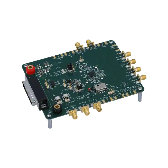
This manual explains how to use the CDCM7005 evaluation module (EVM)
and provides guidelines to build the customer’s own systems. The manual
includes schematics, layout, bill of materials, and a software description.
How to Use This Manual
This document contains the following chapters:
- Chapter 1—Introduction
- Chapter 2—Quick Start
- Chapter 3—EVM Hardware
- Chapter 4—Serial Peripheral Interface (SPI) Software
- Chapter 5—Schematics, Board Layout, and Parts List
Related Documentation From Texas Instruments
-
CDCM7005 Data Sheet, SCAS793, Texas Instruments
FCC Warning
This equipment is intended for use in a laboratory test environment only. It
generates, uses, and can radiate radio frequency energy and has not been
tested for compliance with the limits of computing devices pursuant to subpart
J of part 15 of FCC rules, which are designed to provide reasonable protection
against radio frequency interference. Operation of this equipment in other
environments may cause interference with radio communications, in which
case the user at his own expense will be required to take whatever measures
may be required to correct this interference.
If You Need Assistance. . .
If you need assitance with this device, please email
clocks_apps@list.ti.com
iii
�Contents
������
1
Introduction . . . . . . . . . . . . . . . . . . . . . . . . . . . . . . . . . . . . . . . . . . . . . . . . . . . . . . . . . . . . . . . . . . . . . 1-1
1.1
CDCM7005 Functional Block Diagram . . . . . . . . . . . . . . . . . . . . . . . . . . . . . . . . . . . . . . . . . 1-2
2
Quick Start . . . . . . . . . . . . . . . . . . . . . . . . . . . . . . . . . . . . . . . . . . . . . . . . . . . . . . . . . . . . . . . . . . . . . . 2-1
3
EVM Hardware . . . . . . . . . . . . . . . . . . . . . . . . . . . . . . . . . . . . . . . . . . . . . . . . . . . . . . . . . . . . . . . . . .
3.1
Board View and Connector Location . . . . . . . . . . . . . . . . . . . . . . . . . . . . . . . . . . . . . . . . . .
3.2
Hardware Configuration . . . . . . . . . . . . . . . . . . . . . . . . . . . . . . . . . . . . . . . . . . . . . . . . . . . . .
3.2.1 Power Supply (P1, P2) . . . . . . . . . . . . . . . . . . . . . . . . . . . . . . . . . . . . . . . . . . . . . . .
3.2.2 Onboard Switches and Indicators (SW1−SW2, D1−D4) . . . . . . . . . . . . . . . . . . .
3.2.3 Programming Interfaces (J30, J31) . . . . . . . . . . . . . . . . . . . . . . . . . . . . . . . . . . . .
3.2.4 Loop Filter (J32−J34) . . . . . . . . . . . . . . . . . . . . . . . . . . . . . . . . . . . . . . . . . . . . . . . .
3.2.5 High-Speed Outputs and Inputs (J1−J4, J6−J11, J13, J14, J22, and J23) . . .
3.2.6 VCXO Inputs and Outputs (J16−J18) . . . . . . . . . . . . . . . . . . . . . . . . . . . . . . . . . . .
3.2.7 AC-Coupling at PRI_REF (C1, R4, R6) and SEC_REF (C5, R13, R15) . . . . .
4
Serial Peripheral Interface (SPI) Software . . . . . . . . . . . . . . . . . . . . . . . . . . . . . . . . . . . . . . . . . . 4-1
4.1
Functional Description . . . . . . . . . . . . . . . . . . . . . . . . . . . . . . . . . . . . . . . . . . . . . . . . . . . . . . . 4-2
4.2
Software Installation . . . . . . . . . . . . . . . . . . . . . . . . . . . . . . . . . . . . . . . . . . . . . . . . . . . . . . . . 4-2
5
Application Level Circuit Diagram . . . . . . . . . . . . . . . . . . . . . . . . . . . . . . . . . . . . . . . . . . . . . . . .
5.1
Application Circuit Diagram . . . . . . . . . . . . . . . . . . . . . . . . . . . . . . . . . . . . . . . . . . . . . . . . . .
5.1.1 Passive Loop Filter . . . . . . . . . . . . . . . . . . . . . . . . . . . . . . . . . . . . . . . . . . . . . . . . . .
5.1.2 External Active Loop Filter Using OPA341 . . . . . . . . . . . . . . . . . . . . . . . . . .
5-1
5-2
5-2
5-3
6
Parts List, Board Layouts, and Schematics . . . . . . . . . . . . . . . . . . . . . . . . . . . . . . . . . . . . . . . .
6.1
Parts List . . . . . . . . . . . . . . . . . . . . . . . . . . . . . . . . . . . . . . . . . . . . . . . . . . . . . . . . . . . . . . . . . .
6.2
Board Layout . . . . . . . . . . . . . . . . . . . . . . . . . . . . . . . . . . . . . . . . . . . . . . . . . . . . . . . . . . . . . .
6.3
Schematic . . . . . . . . . . . . . . . . . . . . . . . . . . . . . . . . . . . . . . . . . . . . . . . . . . . . . . . . . . . . . . . . .
6-1
6-2
6-4
6-9
3-1
3-2
3-2
3-2
3-2
3-3
3-3
3-3
3-4
3-4
v
�Contents
�����
3−1
4−1
5−1
5−2
6−1
6−2
6−3
6−4
6−5
6−6
Board View . . . . . . . . . . . . . . . . . . . . . . . . . . . . . . . . . . . . . . . . . . . . . . . . . . . . . . . . . . . . . . . . . . . 3-2
Screen View . . . . . . . . . . . . . . . . . . . . . . . . . . . . . . . . . . . . . . . . . . . . . . . . . . . . . . . . . . . . . . . . . . 4-2
CDCM7005 With a Passive Loop Filter Configuration . . . . . . . . . . . . . . . . . . . . . . . . . 5-2
CDCM7005 With an External Active Loop Filter Using OPA341 . . . . . . . . . . . . . . . . . . . . . 5-3
Component View and Silkscreen (Top Side) . . . . . . . . . . . . . . . . . . . . . . . . . . . . . . . . . . . . . . 6-5
Component View and Silkscreen (Bottom Side) . . . . . . . . . . . . . . . . . . . . . . . . . . . . . . . . . . . 6-6
Top Layer View . . . . . . . . . . . . . . . . . . . . . . . . . . . . . . . . . . . . . . . . . . . . . . . . . . . . . . . . . . . . . . . 6-7
Bottom Layer View . . . . . . . . . . . . . . . . . . . . . . . . . . . . . . . . . . . . . . . . . . . . . . . . . . . . . . . . . . . . 6-8
Ground Plane View . . . . . . . . . . . . . . . . . . . . . . . . . . . . . . . . . . . . . . . . . . . . . . . . . . . . . . . . . . . . 6-9
Power Layer View . . . . . . . . . . . . . . . . . . . . . . . . . . . . . . . . . . . . . . . . . . . . . . . . . . . . . . . . . . . . 6-10
�����
3−1
vi
Filter Configurations . . . . . . . . . . . . . . . . . . . . . . . . . . . . . . . . . . . . . . . . . . . . . . . . . . . . . . . . . . . 3-3
�Chapter 1
������������
The CDCM7005 is a high-performance, low phase noise and low skew clock
synchronizer that synchronizes an on-board voltage controlled crystal
oscillator (VC(X)O) frequency to an external reference clock. The device
operates up to 2.2 GHz. The PLL loop bandwidth and damping factor can be
adjusted to meet different system requirements by selecting the external
VC(X)O, loop filter components, frequency for PFD, and charge pump current.
Each of the five differential LVPECL and five LVCMOS pair outputs can be
programmed by a serial peripheral interface (SPI). The SPI allows individual
control of the frequency and enable/disable state of each output. As the
system requires external components like a loop filter and VC(X)O, this EVM
provides an easy method to evaluate and modify the performance and
parameters of the clock system in conjunction with the specific customer
application. Loop bandwidth can be selected as low as 10 Hz or less, allowing
the device to clean the system’s clock jitter.
In non PLL mode, the CDCM7005 can be used as a simple LVPECL or
LVCMOS buffer with divider options.
Topic
1.1
Page
CDCM7005 Functional Block Diagram . . . . . . . . . . . . . . . . . . . . . . . . . . 1-2
Introduction
1-1
�CDCM7005 Functional Block Diagram
1.1 CDCM7005 Functional Block Diagram
AVCC
VCC
VCC_CP
Selected REF Signal
REF_SEL
Manual &
Automatic
CLK Select
STATUS_REF /
PRI_SEC_CLK
STATUS_VCXO
/ I_REF_CP
freq. detect
> 2 MHz
PLL_LOCK
PRI_REF
LVCMOS
SEC_REF
REF_MUX
freq. detect
> 2 MHz
Reference
Clock
Feedback
Clock
Progr. Delay
M
Progr. Divider
M 210
Progr. Delay
N
Progr. Divider
N 212
LOCK
HOLD
PFD
Charge
Pump
Current
Reference
SPI LOGIC
CTRL_LE
CP_OUT
CTRL_DATA
CTRL_CLK
PECL
to
LVCMOS
LV
CMOS
FB_MUX
RESET or
HOLD
Y0_MUX
Y0A
PD
LV
PECL
Y0B
LV
CMOS
Y1_MUX
LV
CMOS
÷1
Y1A
LV
PECL
Y1B
÷2
LV
CMOS
÷3
LV
CMOS
÷4
VCXO_IN
PECL
INPUT
Y2A
Y2_MUX
VCXO_IN
÷6
Y2B
÷/88
LV
CMOS
÷ 16
÷4
90o
LV
CMOS
Y3A
Y3_MUX
90o
÷8
LV
PECL
P16−Div
P Divider
LV
PECL
Y3B
LV
CMOS
Bias Generator
VCC − 1.3 V
LV
CMOS
Y4A
Y4_MUX
VBB
LV
PECL
Y4B
LV
CMOS
GND
1-2
�Chapter 2
����� �����
In order to setup the EVM quickly and to take some measurements at default
settings, the following actions are required:
- Supply 3.3 V to P1, LED D4 will be on.
- Apply a single-ended reference clock to the reference clock input
PRI_REF (pin A1) or SEC_REF (pin B1). For default setting, the reference
clock must be 1/8th of the VC(X)O frequency. If REF_SEL is set to 1, then
PRI_REF is selected. If REF_SEL is set to 0, then SEC_REF is selected.
This selection can be realized via J26 (header 1 and 2 is high; header 2
and 3 is low).
- Connect Y0/Y0B (or Y1/Y1B) to oscilloscope in order to check an output
signal. Ensure the oscilloscope has 50 Ω to ground termination.
After power up, D1 is on if there is a valid reference clock and D2 is on if there
is a valid VC(X)O clock for the CDCM7005. If D3 turns on, then the reference
clock and the VC(X)O clocks are phase locked.
Quick Start
2-1
�Chapter 3
��� ��������
This chapter discusses the EVM hardware.
Topic
Page
3.1
Board View and Connector Location . . . . . . . . . . . . . . . . . . . . . . . . . . . . 3-2
3.2
Hardware Configuration . . . . . . . . . . . . . . . . . . . . . . . . . . . . . . . . . . . . . . . 3-2
EVM Hardware
3-1
�Board View and Connector Location
3.1 Board View and Connector Location
Figure 3−1. Board View
3.2 Hardware Configuration
This section describes the board configuration using on-board jumpers and
solder bridges.
3.2.1
Power Supply (P1, P2)
- Supply 3.3 V ±10% on P1 and P2 using a stabilized external power supply.
J
3.2.2
WARNING: Never supply more than 3.6 V on P1.
Onboard Switches and Indicators (SW1−SW2, D1−D4)
- Push SW1 to enter the power-down mode of the CDCM7005 device. Then
all current sources are switched off, all outputs are switched into 3-state,
and all dividers (M, N, and P) are reset to default.
- Push SW2 to enter the reset mode of the device. The charge pump (CP)
is switched to 3-state and all counters (N, M, P) are rest to zero (the initial
divider settings are maintained in SPI.
- The three status outputs of the CDCM7005 are fed to LED indicators. D1
on indicates a valid reference input clock signal. D2 is on if the VC(X)O
input clock is valid and D3 turns on if the PLL has been locked.
- D4 indicates power supply
Note:
In case of a low input impedance of the VC(X)O control voltage input, there
is a possibility D3 may not turn on to indicate locking.
3-2
�Hardware Configuration
3.2.3
Programming Interfaces (J30, J31)
The SPI of the device is used for writing to the control register of the device.
It consists of three control lines CTRL_CLK, CTRL_DATA, and CTRL_LE.
There are four 30-bit wide RAM registers, which can be addressed by the two
LSBs of a transferred word. Every transmitted word must have 32 bits, starting
with MSB. After supplying power or activating the power-down mode, the
registers are loaded with the device default values internally (see the
CDCM7005 data sheet, SCAS793). However, if specific register settings are
required for any applications, there are two ways to program the device
externally:
- Connect the parallel port cable to the PC and EVM parallel port. This
needs control S/W (see Chapter 4).
3.2.4
Loop Filter (J32−J34)
The loop filter is one of the key elements determining the loop bandwidth of
the PLL. The loop filter converts the charge pump current into the control
voltage for the voltage controlled oscillator. The phase difference between the
input clocks of the phase frequency detector determines the width of the
charge pump output current pulses. These high frequency pulses are
transformed into a voltage to control the oscillator.
Basically, three types of loop filters are implemented on the EVM.
- Passive loop filter
- External active loop filter using an external low-noise OPA.
Filter types can be selected by soldering bridges J32−J34, see Table 3−1.
Control voltage of the VC(X)O can be measured at J9 or TP1. If an external
OPA is used, it needs to be switched on by connecting J34. For example,
passive filter operation is provided when pads 1 and 3 of J33 are solder bridged
and pads 1 and 3 of J32 are solder bridged.
Default setting: Passive Loop Filter
Table 3−1. Filter Configurations
Bridge
Passive Filter
Active With An External OPA
J33
1−3
1−2
J34
Open
Closed
J32
1−3
1−2
3.2.5
High-Speed Outputs and Inputs (J1−J4, J6−J11, J13, J14, J22, and J23)
The CDCM7005 drives five differential LVPECL outputs. All PECL outputs are
ac-coupled and terminated with 150 Ω to GND. This is in contrast to typical
LVPECL termination, which requires VCC − 2 V as termination voltage. The
reason is to simplify the power supply scheme. The device output’s trace
impedance is 50 Ω and traces are matched in length. All outputs have options
for pullup and pulldown resistors.
EVM Hardware
3-3
�Hardware Configuration
When the CDCM7005 is powered up, it defaults to five LVPECL outputs.
However, this EVM is configured as follows:
- Y0 − Y2 = LVPECL
- Y3, Y4 = LVCMOS (in addition Y4 has an option for a custom filter)
The reference input clock signal has to be applied to J1 or J6. The reference
input clock signal can be sensed on J4. In this case, close the bridge J5 (the
oscilloscope’s 50 Ω may be used to terminate the 50-Ω trace). The reference
input clock sense line is matched to the LVPECL outputs line to avoid any
additional delay offset. The input is ac-coupled (C4).
3.2.6
VC(X)O Inputs and Outputs (J16−J18)
The CDCM7005 requires an external VC(X)O in order to complete the PLL
loop. The VC(X)O adjusts the frequency and phase depending on the control
voltage level coming from the loop filter and provide the input clock to the
LVPECL block.
Another option would be to use an external source via J16 and J18.
3.2.7
AC-Coupling at PRI_REF (C1, R4, R6) and SEC_REF (C5, R13, R15)
An ac-coupling is provided at PRI_REF and SEC_REF to ease the use of the
CDCM7005 with different signaling levels (LVCMOS, LVPECL, LVDS,...).
However, the ac-coupling will increase the PLL stabilization time after power
up due to transient effects. It also increases the switching time between
PRI_REF and SEC_REF in case of automatic reference clock switching.
Therefore, the ac-coupling must be removed for optimized system
performance (C1 and C5 has to be replaced with an 0-Ω resistor and R4, R6,
R13, and R15 have to be removed).
3-4
�Chapter 4
������ ���������� �����!��� "���# ��!�����"$#
This chapter discusses the serial peripheral interface software.
Topic
Page
4.1
Functional Description . . . . . . . . . . . . . . . . . . . . . . . . . . . . . . . . . . . . . . . . 4-2
4.2
Software Installation . . . . . . . . . . . . . . . . . . . . . . . . . . . . . . . . . . . . . . . . . . 4-2
1) Copyright 2005 National Instruments Corporation. All Rights Reserved.
Copyright 2005 Texas Instruments Incorporated. All Rights Reserved.
Serial Peripheral Interface (SPI) Software (1)
4-1
�Functional Description
4.1 Functional Description
Programming software here as described is intended for programming the
internal control register of the CDCM7005. The software runs under Windows
2000 / XP / XP *64. A quick installation is required prior to use. See the
Software Installation section.
There are several cases where programming is mandatory.
As a rule of thumb here are some examples:
- Use of active loop filter
- Change of divider ratio or disable of certain LVPECL/LVCMOS outputs
- Select between LVPECL or LVCMOS output
- Change of phase offset, (Delay M/N), or selection of 90’ or 180’ phase shift
- Change of charge pump output current.
- Widening the lock detect window
Figure 4−1. Screen View
4.2 Software Installation
Follow the steps below in order to install the SPI control software:
1)
2)
3)
4)
4-2
Download the CDCM7005 SPI Software from the TI Website (www.ti.com)
Run program setup.exe
Reboot your computer
Run the software from Start −> Programs −> CDCM7005 SPI
�Chapter 5
%����������
������ &�����'
This chapter discusses the application circuit diagram.
Topic
5.1
Page
Application Circuit Diagram . . . . . . . . . . . . . . . . . . . . . . . . . . . . . . . . . . . . 5-2
Application Circuit Diagram
5-1
�Application Circuit Diagram
5.1 Application Circuit Diagram
The following applications sections the two loop filter configurations are
discussed.
5.1.1
Passive Loop Filter
The passive loop filter is a second order filter (two poles, one zero). The zero
is required for the overall loop stability. R1, C1, and C2 generate the dominant
pole of the system. A second pole is introduced by R2 and C3.
Figure 5−1. CDCM7005 With a Passive Loop Filter Configuration
Low-Pass Filter
R2
160 Ω
VC(X)O
491.52 MHz
V_CTRL
PECL_OUT_B
PECL_OUT
C3
100 nF
CDCM7005
PRI_REF
SEC_REF
R1
4.7 kΩ
C2
100 nF
CP_OUT
VCC
VCC
C1
22 µF
CTRL_LE
CTRL_DATA
CTRL_CLK STATUS_REF
STATUS_VC(X)O
PLL_LOCK
SPI
10 nF
130 Ω
YnA
130 Ω
10 nF
VC(X)O_IN
VC(X)O_IN_B
R
82 Ω
5-2
R
82 Ω
YnB
R
150 Ω
R
150 Ω
�Application Circuit Diagram
5.1.2
External Active Loop Filter Using OPA341
Figure 5−2. CDCM7005 With a External Active Loop Filter Using OPA341
Low-Pass Filter
R3
10 kΩ
VC(X)O
491.52 MHz
PECL_OUT_B
PECL_OUT
V_CTRL
C3
100 nF
Vcc
R2
4.7 kΩ
C2
10 µF
Vcc
CDCM7005
R5
10 kΩ
PRI_REF
InN
R1
180 Ω OPA341 Out
InP
SEC_REF
CP_OUT
CTRL_LE
STATUS_REF
CTRL_DATA STATUS_VC(X)O
CTRL_CLK
PLL_LOCK
SPI
VCC
R6
10 kΩ
C1
100 nF
VCC
130 Ω
130 Ω
R
82 Ω
C1
100 nF
YnA
VC(X)O_IN
VC(X)O_IN
R
82 Ω
YnB
R
150 Ω
10 nF
10 nF
R
150 Ω
Application Circuit Diagram
5-3
�Chapter 6
���� (� �) *���� (�+���) ��� ����'����
This chapter contains the parts list, board layout, and schematics for the
CDCM7005 EVM.
Topic
Page
6.1
Parts List . . . . . . . . . . . . . . . . . . . . . . . . . . . . . . . . . . . . . . . . . . . . . . . . . . . . . 6-2
6.2
Board Layout . . . . . . . . . . . . . . . . . . . . . . . . . . . . . . . . . . . . . . . . . . . . . . . . . 6-4
6.3
Schematics . . . . . . . . . . . . . . . . . . . . . . . . . . . . . . . . . . . . . . . . . . . . . . . . . . . 6-8
Parts List, Board Layout, and Schematics
6-1
�Parts List
6.1 Parts List
Item QTY
Reference
Designator
C1−C9, C12,
C13, C15, C17,
C26, C40, C41,
C46, C47, C53,
C54, C56−C58,
C66
C72, C10
Footprint
Part
smd_cap_0402
10 nF
Panasonic
ECJ−0EB1E103K
smd_cap_0402
100 nF
smd_cap_0402
100 pF
Panasonic
ECJ−0EB1E104K
Panasonic
ECJ−0EB1E101K
smd_cap_0402
0Ω
1
24
2
2
3
7
4
2
C11, C32,
C62−C64, C68,
C73
C14, C16
5
1
C18
smd_cap_0402
1000 pF
6
1
C19
smd_cap_0603
1 µF
7
2
C20, C22
smd_cap_0402
0.1 µF
8
1
C21
smd_cap_0402
10 nF
9
1
C23
smd_cap_0402
NU 1.1 pF
10
1
C24
smd_cap_0402
22 pF
11
1
C25
smd_cap_0402
NU 1 pF
12
7
smd_cap_0805
0.1 µF
13
1
C27−C29, C75,
C76, C79, C80
C30
smd_cap_1210
22 µF
14
1
C31
smd_cap_0402
22 nF
15
3
C33−C35
smd_cap_0402
10 nF
16
4
C36, C42, C48,
C49
C49
smd_cap_1210_pol
22 µF
smd_cap_1210_pol
22 µF
smd_cap_1210_pol
10 µF
smd_cap_0402
100 nF
smd_cap_0402
smd_cap_0402
smd_cap_0402
33 nF
2.2 nF
10 pF
17
5
18
3
C37, C43, C50,
C55, C65
C38, C44, C51
19
20
21
3
4
3
C39, C45, C52
C59−C61, C67
C69−C71
6-2
Part Number
Panasonic
ERJ−2GE0R00X
Panasonic
ECJ−0EB1E102K
Panasonic
ECJ−1VF1C105Z
Panasonic
ECJ−0EB1A104K
Panasonic
ECJ−0EB1E103K
NU Rohm
MCH155A1R1CK
Panasonic
ECJ−0EC1H220J
NU Rohm
MCH155A1R1CK
Panasonic
ECP−U1C104MA5
Murata
GRM32ER71A226KE20L
Panasonic
ECJ−0EB1E104K
Panasonic
ECJ−0EF1H103Z
Panasonic
ECS−T1CC226R
Panasonic
ECS−T1CC226R
Panasonic
ECS−H1CC106R
Yageo
04022F104Z7B20D
AVX 0402YD333KAT2A
AVX 0402YC223KAT2A
Panasonic
ECD−G0E100C
�Parts List
Item QTY
22
2
Reference
Designator
Footprint
Part
Part Number
C74
smd_cap_1210
10 µF
Murata
GRM32DR61E106KA12L
C77
smd_cap_1210
10 µF
Murata
GRM32DR61E106KA12L
23
1
C78
smd_cap_0805
NU
Panasonic
ECP−U1C104MA5
24
25
3
1
D1−D3
D4
smd_led_1206
smd_led_1206
Amber
GREEN
Lite−On LTST−C150AKT
Lite−On
LTST−C150KGKT
26
27
1
7
FLT1
J1−J4, J6−J8
ts−38s
sma_alt
TS−38S
SMA
Toyocom Filter
Johnson Comp
142−0701−841
28
1
J5
jumper2
HEADER 2
29
9
sma_alt
NU_SMA
30
4
J9−J11, J13,
J14, J16, J18,
J22, J23
J12, J25, J26,
J27
hdr3_100ctr
HDR3
31
2
J17, J15
smd_bridge_0402
SMD3P_BRIDGE Panasonic
ERJ−2GE0R00X
32
33
1
2
J19
J21, J20
jumper2
smd_bridge_0402
HDR2
Header 2 pos, 0.1 ctr
SMD3P_BRIDGE Panasonic
ERJ−2GE0R00X
34
35
3
1
J24, J28, J29
J30
jumper2
dcon25m
HDR2
PARALLEL
PORT
Header 2 pos, 0.1 ctr
SPC Technology
DB−25P−PCB
36
37
1
2
J31
J33, J32
jumper4
JUMPER3_SMD_WVIA_CD
C7005
HDR4
HDR 3_cdc7005
Header 4 pos, 0.1 ctr
Use 0 W to short pins
(see assy dwg)
38
39
1
1
J34
L1
jumper2
smd_cap_0603
HDR2
75 Ω at100 MHz
Header 3 pos, 0.1 ctr
Murata
BLM18BA750SN1D
40
1
L2
smd_cap_0603
470 nH
Murata
LQW18ANR47J00D
41
2
L4, L3
smd_cap_0603
180 nH
Panasonic
ELJ−FJR18JF2
42
3
L5−L7
smd_cap_0603
75 Ω at 100 MHz
Murata
BLM18BA750SN1D
43
1
L8
smd_cap_0805
2.2 nH
J W Miller Magnetics
PM0805−2N2M
44
45
46
1
1
18
banana_jack
banana_jack
smd_res_0402
PWR_IN
GND
NU 100 Ω
47
2
P1
P2
R1, R2, R7, R9,
R10, R11, R16,
R18−R20, R22,
R24, R26, R27,
R30, R35, R48,
R50
R3, R12
smd_res_0402
NU
Johnson Comp
142−0701−841
Header 3 pos, 0.1 ctr
SPC Technologies 845R
SPC Technologies 845B
Panasonic
ERJ−2RKF1000X
Panasonic
ERJ−2GEJ510X
Parts List, Board Layout, and Schematics
6-3
�Parts List
Item QTY
Reference
Designator
R4, R6, R13, R15,
R62, R63, R65
R5, R8, R14, R17,
R21, R23
R25, R57, R59,
R60, R68−R71,
R74, R75
R28, R45
Footprint
Part
smd_res_0402
100 Ω
smd_res_0402
150 Ω
smd_res_0402
10 kΩ
smd_res_0402
NU 0 Ω
R29, R32, R49,
R80
R38, R31
smd_res_0402
NU 150 Ω
smd_res_0402
130 Ω
smd_res_0402
0Ω
smd_res_0402
82 Ω
48
7
49
6
50
10
51
2
52
4
53
2
54
10
55
2
R33, R34, R41,
R42, R82,−R87
R43, R36
56
57
2
2
R37, R44
R39, R40
smd_res_0402
smd_res_0402
NU
62 W
58
2
R47, R46
smd_res_0402
NU 100
59
4
smd_res_0402
100 kΩ
60
1
R51, R64, R66,
R67
R52
smd_res_0402
160 Ω
61
2
R53, R72
smd_res_0402
4.7 kΩ
62
3
R54−R56
smd_res_0402
750
63
1
R58
smd_res_0402
NU 12K 1%
64
1
R61
smd_cap_0402
1.5 kΩ
65
1
R73
smd_res_0402
180 Ω
66
3
R78, R79, R81
smd_res_0402
22 Ω
67
2
SW2, SW1
switch_reset
68
69
2
1
TP1, TP2
U2
testpin_30dia
mbga_pt8mm_64_skt
SW
PUSHBUTTON
T POINT R
CDCM7005
70
1
U3
soic14
SN74LV125
71
72
1
1
U4
U5
soic_round_4
soic8
NU SGA−4586
OPA341
73
74
1
4
VCXO1
MP3
VCXO_6
STAND OFF
VCXO_6
75
4
MP2
SCREW
6-4
Part Number
Panasonic
ERJ−2RKF1000X
Panasonic
ERJ−2RKF1500X
Panasonic
ERJ−2RKF1002X
Panasonic
ERJ−2GE0R00X
Panasonic
ERJ−2RKF1500X
Panasonic
ERJ−2GEJ131X
Panasonic
ERJ−2GE0R00X
Panasonic
ERJ−2GEJ820X
NU
Panasonic
ERJ−2GEJ620X
Panasonic
ERJ−2RKF1000X
Panasonic
ERJ−2RKF1003X
Panasonic
ERJ−2RKF1002X
Panasonic
ERJ−2RKF1472X
Panasonic
ERJ−2GEJ131X
Panasonic
ERJ−2RKF4121X
Panasonic
ERJ−2RKF1501X
Panasonic
ERJ−2RKF1472X
Panasonic
ERJ−2GEJ220X
KT11P3JM
Test point
Texas Instruments
CDCM7005
Texas Instruments
SN74LV125AD
NU Sirenza SGA−4586
Texas Instruments
OPA341UA
Toyocom VCXO
Legs for PCB
Legs for PCB
�Board Layout
6.2 Board Layout
Figure 6−1. Component View and Silkscreen (Top View)
Parts List, Board Layout, and Schematics
6-5
�Board Layout
Figure 6−2. Component View and Silkscreen (Bottom View)
6-6
�Board Layout
Figure 6−3. Top Layer View
Parts List, Board Layout, and Schematics
6-7
�Board Layout
Figure 6−4. Bottom Layer View
6-8
�Board Layout
Figure 6−5. Ground Plane View
Parts List, Board Layout, and Schematics
6-9
�Board Layout
Figure 6−6. Power Layer View
6-10
�A
B
5
1 1
GND
P2
PW R_IN
1 1
R61
1.5K
D4
GREEN
PWR_IN
GND
L7
VCC
C48
22uF
4
GND
C51
100n
C44
100n
C50
10uF
GND
C38
100n
C49
22uF
1
2
75 OHM @ 100MHZ
C43
10uF
C42
22uF
C37
10uF
1
2
P1
GND
AVCC
1
2
75 OHM @ 100MHZ
L6
C36
22uF
VCC_CP
1
2
75 OHM @ 100MHZ
L5
1
2
1
2
C
1
12
2
1
2
1
2
1
1
2
2
1
2
1
2
1
2
C45
33n
C52
33n
3
C53
10n
C46
10n
3
C40
10n
C39
33n
1
1
2
1
2
1
2
1
2
2
1
2
4
VCC
1
C56
C55 10n
10uF
C65
10uF
AVCC
2
1
2
1
2
1
2
C66
10n
C58
10n
C68
100P
C57
10n
GND
C67
2.2n
2
1
2
1
2
1
2
1
1
2
2
C59
2.2n
2
1
2
C60
2.2n
1
2
Parts List, Board Layout, and Schematics
1
1
45
of Sheet
A
CDCM7005EVM_QFN−SCH
Tuesday, April 26, 2005
Document Number
CDCM7005_QFN Evaluation Module
GND
C62 C63 C64
100P 100P 100P
D a te:
Size
B
Title
C61
2.2n
2
1
2
1
2
1
D
5
A
B
C
D
Schematics
6.3 Schematics
The following pages contain the schematics for the CDCM7005 (QFN
package).
6-11
�A
B
C
D
VCC
2
5
GND
R 57 10K
1
1
2
J26 3
VCC_CP
AVCC
1
2
C32100P AVCC
C3122n
1
2
CTRL_LE
CTRL_CLK
CP_OUT
GND
SEC_REF
REF_SEL PRI_REF
VBB
VCXO_IN
VCXO_INB
Y0B
Y0
4
34 NC
33 VCC_CP
32 AVCC
31 CP_OUT
30 AVCC
29 CTRL_LE
28 CTRL_CLK
27 AVCC
37 SEC_REF
36 PRI_REF
35 REF_SEL
43 VCXO_IN
42 VCXO_INB
40 VBB
39 AVCC
38 AVCC
47 Y0B
46 Y0A
4
U2
Y4
Y4B
STAT_VCXO/I_REF_CP
Y3
Y3B
Y2
Y2B
Y1
Y1B
J27
CDCM7005
3
GND
10nC33
1
2
J25
R 54
2
2
GND
1
10n
1
J29 2
GND
GND
SW2
1
GND
1
of
35 Sheet
CDCM7005EVM_QFN−SCH A
Document Number
Tuesday, April 26, 2005
D a te:
CDCM7005_QFN Evaluation Module
GND
RST
SW1
Size
B
Title
10n C35
2
10KR60
1
2
1
J28 2
PWRDWN
C34
2
1
10KR59
1
2
750 Amber D1
1 1
2
STAT_VCXO
2
R 56
2
Amber D3
1 1
2
750
GND
RESET
R58
NU 12K 1%
1
2
PW R_ DW N
22
R 55
750 Amber D2
STATUS_VCXO or I_REF_CP
23
2
1 1
2
STATUS_REF or PRI_SEC_CLK
GND 24
GND
GND
PLL_LOCK
PLL_LOCK 25
CTRL_DATA
CTRL_DATA 26
PLLLOCK
Y4A 16
Y4B 17
Y3A 11
Y3B 12
/RESET or /HOLD14
Y2A 7
Y2B 8
/PD 1
Y1A 3
Y1B 4
3
1
2
3
6-12
1
2
3
5
A
B
C
D
Rev
Schematics
�A
B
C
5
GND
.1uF
C27
2
1
V CHECK
J24
V_CTRL
1 R51 2
100K
V_CTRL
2
1
3
R52 2
160
4
C28
.1uF
1
J32
C29
.1uF
GND
C30
22uF
R53
4.7K
R70 2
10K
GND
.1uF
C76
1
GND
3
.1uF
C79
2
1
C77
R72
2
1 1
2
4.7K
10uF C78
2
1
NU
J33
R73
180
R71 10K
2
1
C74
10uF
6
OPA341
GND
.1uF
C75
− 2
+ 3
CP_OUT
U5
GND
L8
2.2nH
VCC
J34
2
1
4
2
1
2
1
2
1
5
7
8
4
1
2
2
VCC
R74
10K
1
2
Passive Filter (Default Setting): short pin 1 & 3 on J3 2, J33
pin 1 & 2 on J32, J33, J34
Active Filter w/ External Op Amp: short
2
1
3
1
2
2
1
2
2 1
1
1
2
3
1
2
R75
10K
2
.1uF
C80
GND
1
1
2
D
5
Parts List, Board Layout, and Schematics
1
of
15 Sheet
CDCM7005EVM_QFN−SCH A
Document Number
Tuesday, April 26, 2005
D a te:
CDCM7005_QFN Evaluation Module
Size
B
Title
1
A
B
C
D
Rev
Schematics
6-13
�A
B
C
Y4B
Y3B
Y2B
Y1B
1
R80
NU 150
Y4
Y3
Y2
R49
NU 150
GND
R21
150
R8
150
R23
150
1 R87 2
0 ohm
1 R86 2
0 ohm
GND
GND
GND
1
10n
2
C9
1
C8
1
R11
NU 100
1 R88 2 Y1_SMA
0 ohm
GND
R9
NU 100
GND
1
2
SMA
J7
2
2
GND
SMA
J3
NU_SMA
J10 GND
1 R91 2Y2B_SMA
1
2
0 ohm
R24
NU_SMA
NU 100
J11
GND
R22
NU 100
R20
R90
NU 100 1
2 Y2_SMA
1
0 ohm
VCC
GND
R19
NU 100
VCC
GND
10n
2
10n
2
VCC
VCC 1
GND
1
NU 100
R50
2
NU 100
R48
R40
** 62
** .1uF
GND C22
1
2
C20
** .1uF
GND
4
2
NU_SMA
J23
GND
L4
** 180nH
OUT 5
** TS−38S
FLT1
1 IN
C23
** NU 1.1pF
L3
** 180nH
GND
J19
** 75 ohm@100MHz
1
2
L1
C19
** 1uF
GND
** 1000pF
C18
GND
1 R94 2 Y4B_SMA
1
0 ohm
L2
** 470nH
R39
** 62
SGA−4586 J21
U4
GND
3
Def ault setting
Amp Bypass :
S hort pin 1&2
of J18 & J22
GND
1 R81 2 1
2
22 ohm
C 26 10n2
5
C6
1
10n
2
VCC
Y0_SMA
1 R76 2
1
2
0 ohm
NU 100 R2
SMA
R7
J2
GND
NU 100
1 R77 2Y0B_SMA
1
0 ohm
R1
NU 100
VCC
GND
R10
NU 100 VCC
C3
1
10n
2
R16
1 R85 2 1
2
1 R89 2Y1B_SMA 1
2
0 ohm
NU 100
0 ohm
R17
C7
10n
SMA
R18
150
J8
GND
GND
NU 100
GND
1 R84 2
0 ohm
1 R83 2
0 ohm
C2
1
VCC
4
3
GND
GND
VCC
1
C25
** NU 1pF
2
TP2
GND
3
2
GND
TP1
NU_SMA
J22 GND
2
2 VCXO_INB_SMA
10n
2 VCXO_IN_SMA
2
2
2
GND
2
GND
J15 2
1 J17
3
3
1
1
2
C11100P
GND
GND
VCC
GND
VCC
VBB
GND
VBB
2
2
1
82
130
1
NU 0 ohm
2
R28
R43
2
R45
1
NU 0 ohm
1
82
R 38 130
1
1
SEC_REF
PRI_REF
VCXO_IN
VCXO_INB
1
of
25 Sheet
CDCM7005EVM_QFN−SCH A
Document Number
Tuesday, April 26, 2005
D a te:
CDCM7005_QFN Evaluation Module
2
0 ohm
VCC
Size
B
Title
R41
1
0 ohm
2
1
R44
NU
C16
R42
2
1 1
0 ohm
1
J5
HEADER 2
1
2
VCC R 31
C14
2
2
0 ohm 2
R36
GND
1 R13 2
100
1 R15 2
100
1 R4
2
100
1 R6
2
100
R33
R34
1 2
1 1
0 ohm
0 ohm
2
1
R37
NU
2
V_CTRL
C10100n
1
2
10n
2
10n
VCC
C5
1
C4
VCXO1
1 V_CTRLVCC 6
2 EN
OUTB 5
3 GND OUT 4
VCXO_6
10n
C17
1 VCXO_IN_EXT
1
NU_SMA
10n
C1
2
2
1
V_CTRL
R12 NU
NU_SMA
1
J9
GND
SEC_ REFCLK
1
2
C15
1 VCXO_INB_EXT
1
NU_SMA
J18
GND
SMA
1
NU
PRI_CLK_SENSE
1
R3
PRI_REFC LK
1
2
GND
J6
1
R 25 10K
1
1
2
J12 3
2
J16
2
GND
VCC
1
SMA
J1
SMA J4
GND
GND
2
GND
2
1 R95 2 Y4_SMA 1
0 ohm
2
R47
** NU 100
** 22pFC24
2
R46
** NU 100
VCC
3
GND
GND
VCC
R26
NU 100
C 12 10n
R27
NU 100
1 R78 2
1
2
1 R92 2 Y3_SMA
1
2
22 ohm
0 ohm
R29
R30
R93
NU_SMA
NU 150
NU 100 1
Y3B_SMA 1
J13 GND
1 R79 2
1
2
2
2
22 ohm
0 ohm
R32
C 13 10n
NU_SMA
NU 150
R35
NU 100
J14
GND
J20
1
C21 ** 10n
1
2
GND
R14
150
1
D
3
2
1
2
Y1
1
R5
150
3
2
4
2
1
1 2
2
1
2
1
2
Y0
1 R82 2
0 ohm
1
2
1
2
1
2
2
1
2
1
1
1 2
2
Y0B
1
2
2
1
1
1
1
2
1
2
1
1 2
2
3
3
1
2
1
2
2
1
3
3
3
1
1
2
2
2
2
3
2
1
2
1
2
1
2
1
2
1
2
1
2
3
2
1
2
3
3
3
1
2
1
2
3
3
3
1
2
1
2
1
2
3
OUT
OUTB
6-14
3
5
A
B
C
D
Rev
Schematics
�A
B
C
5
4
C 70
1
1
R63
100
10p
GND
SPI_DATA
SPI_CLK
SPI_LE
2
2
1
2
R62
100
10p
C 71
1
2
C 69 10p
1
2
1
J31 2
3
4
HDR4
GND
4
1
1
2
3
4
5
6
7
8
9
10
11
12
13
2
GND
3
VCC
10KR69
1
2
GND
DATA
VCC
R 68 10K
1
VCC
3
1OE VCC 14
1A
4OE 132
1Y
4A 12
2OE 4Y 11
3OE 10
2A
2Y
3A 9
GND 3Y 8
SN74LV125U3
1
2
C73100P
C72100n
1
2
14
J30 15
16
17
18
19
20
21
22
23
24
25
26
27
1
2
3
4
5
6
7
VCC
R 67 100K
1
R 66 100K
1
GND
2
R64 100K
1
GND
CLK
LE
R65
100
2
CTRL_DATA
CTRL_CLK
CTRL_LE
PARALLEL PORTGND
2
D
5
2
2
Parts List, Board Layout, and Schematics
1
of
55 Sheet
CDCM7005EVM_QFN−SCH A
Document Number
Tuesday, April 26, 2005
D a te:
CDCM7005_QFN Evaluation Module
Size
B
Title
1
A
B
C
D
Rev
Schematics
6-15
�