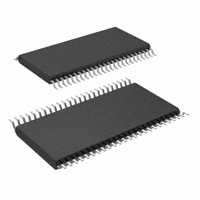
CDCV857
2.5-V PHASE LOCK LOOP CLOCK DRIVER
SCAS645A – AUGUST 2000 – REVISED OCTOBER 2000
D
D
D
D
D
D
D
D
D
D
Phase-Lock Loop Clock Driver for Double
Data-Rate Synchronous DRAM
Applications
Spread Spectrum Clock Compatible
Operating Frequency: 60 to 200 MHz
Low Jitter (cyc–cyc): ±75 ps
Distributes One Differential Clock Input to
Ten Differential Outputs
Three-State Outputs When the Input
Differential Clocks Are 20 MHz input signal this detection circuit turns on the PLL again and
enables the outputs.
When AVDD is strapped low, the PLL is turned off and bypassed for test purposes. The CDCV857 is also able
to track spread spectrum clocking for reduced EMI.
Since the CDCV857 is based on PLL circuitry, it requires a stabilization time to achieve phase-lock of the PLL.
This stabilization time is required following power up. The CDCV857 is characterized for operation from 0°C
to 85°C.
Please be aware that an important notice concerning availability, standard warranty, and use in critical applications of
Texas Instruments semiconductor products and disclaimers thereto appears at the end of this data sheet.
Copyright 2000, Texas Instruments Incorporated
PRODUCTION DATA information is current as of publication date.
Products conform to specifications per the terms of Texas Instruments
standard warranty. Production processing does not necessarily include
testing of all parameters.
POST OFFICE BOX 655303
• DALLAS, TEXAS 75265
1
�CDCV857
2.5-V PHASE LOCK LOOP CLOCK DRIVER
SCAS645A – AUGUST 2000 – REVISED OCTOBER 2000
FUNCTION TABLE
(Select Functions)
INPUTS
OUTPUTS
PLL
AVDD
GND
PWRDWN
CLK
CLK
Y[0:9]
Y[0:9]
FBOUT
FBOUT
H
L
H
L
H
L
H
Bypassed/Off
GND
H
H
L
H
L
H
L
Bypassed/Off
X
L
L
H
Z
Z
Z
Z
Off
X
L
H
L
Z
Z
Z
Z
Off
2.5 V (nom)
H
L
H
L
H
L
H
On
2.5 V (nom)
H
H
L
H
L
H
L
On
2.5 V (nom)
X
VDDQ) . . . . . . . . . . . . . . . . . . . . . . . . . . . . . . . . . . . . . . . . . . ±50 mA
Continuous output current, IO (VO = 0 to VDDQ) . . . . . . . . . . . . . . . . . . . . . . . . . . . . . . . . . . . . . . . . . . . . ±50 mA
Continuous current to GND or VDDQ . . . . . . . . . . . . . . . . . . . . . . . . . . . . . . . . . . . . . . . . . . . . . . . . . . . . . ±100 mA
Package thermal impedance, θJA (see Note 3): DGG package . . . . . . . . . . . . . . . . . . . . . . . . . . . . . . . . 89°C/W
Storage temperature range Tstg . . . . . . . . . . . . . . . . . . . . . . . . . . . . . . . . . . . . . . . . . . . . . . . . . . . –65°C to 150°C
† Stresses beyond those listed under “absolute maximum ratings” may cause permanent damage to the device. These are stress ratings only, and
functional operation of the device at these or any other conditions beyond those indicated under “recommended operating conditions” is not
implied. Exposure to absolute-maximum-rated conditions for extended periods may affect device reliability.
NOTES: 1. The input and output negative voltage ratings may be exceeded if the input and output clamp-current ratings are observed.
2. This value is limited to 3.6 V maximum.
3. The package thermal impedance is calculated in accordance with JESD 51.
POST OFFICE BOX 655303
• DALLAS, TEXAS 75265
3
�CDCV857
2.5-V PHASE LOCK LOOP CLOCK DRIVER
SCAS645A – AUGUST 2000 – REVISED OCTOBER 2000
recommended operating conditions (see Note 4)
MIN
Supply voltage, VDDQ, AVDD
TYP
PWRDWN
CLK, CLK, FBIN, FBIN
High level input voltage,
voltage VIH
PWRDWN
V
–0.3
VDDQ/2 – 0.18
0.7
V
VDDQ/2 + 0.18
1.7
DC input signal voltage (see Note 5)
VDDQ + 0.3
VDDQ
–0.3
Differential input signal voltage
voltage, VID (see Note 6)
DC
CLK, FBIN
0.36
AC
CLK, FBIN
0.7
Output differential cross-voltage, VOX (see Note 7)
Input differential pair cross-voltage, VIX (see Note 7)
UNIT
2.7
CLK, CLK, FBIN, FBIN
Low level input voltage
voltage, VIL
MAX
2.3
VDDQ/2 – 0.2
VDDQ/2 – 0.2
High-level output current, IOH
VDDQ + 0.6
VDDQ + 0.6
VDDQ/2
VDDQ/2 + 0.2
VDDQ/2 + 0.2
–12
Low-level output current, IOL
V
V
V
V
V
mA
12
mA
Input slew rate, SR
1
4
V/ns
Operating free-air temperature, TA
0
85
°C
NOTES: 4. Unused inputs must be held high or low to prevent them from floating.
5. DC input signal voltage specifies the allowable dc execution of differential input.
6. Differential input signal voltage specifies the differential voltage |VTR – VCP| required for switching, where VTR is the true input level
and VCP is the complementary input level.
7. Differential cross-point voltage is expected to track variations of VCC and is the voltage at which the differential signals must be
crossing.
4
POST OFFICE BOX 655303
• DALLAS, TEXAS 75265
�CDCV857
2.5-V PHASE LOCK LOOP CLOCK DRIVER
SCAS645A – AUGUST 2000 – REVISED OCTOBER 2000
electrical characteristics over recommended operating free-air temperature range (unless
otherwise noted)
PARAMETER
TEST CONDITIONS
All inputs
VDDQ = 2.3 V,
II = –18 mA
VDDQ = min to max, IOH = –1 mA
MIN
TYP†
MAX
UNIT
–1.2
V
VIK
Input voltage
VOH
High level output voltage
High-level
VOL
Low level output voltage
Low-level
IOH
IOL
VO
Output voltage swing
VOX
Output differential
cross-voltagew
II
Input current
VDDQ = 2.7 V,
VI = 0 V to 2.7 V
±10
µA
IOZ
High-impedance-state
output current
VDDQ = 2.7 V,
VO= VDDQ or GND
±10
µA
IDDPD
Power down current on
VDDQ + AVDD
CLK and CLK = 0 MHz; PWRDWN = Low;
Σ of IDD and AIDD
100
200
µA
fO = 200 MHz
330
Dynamic current on VDDQ
all outputs loaded
as shown in
Figure 3
275
IDD
fO = 167 MHz
250
300
AIDD
Supply current on AVDD
fO = 200 MHz
fO = 167 MHz
10
12
8
10
VDDQ = 2.3 V,
IOH = –12 mA
VDDQ = min to max, IOL = 1 mA
High-level output current
VDDQ = 2.3 V,
VDDQ = 2.3 V,
IOL = 12 mA
VO = 1 V
Low-level output current
VDDQ = 2.3 V,
VO = 1.2 V
Differential outputs are terminated with
120 Ω
VDDQ– 0.1
1.7
V
0.1
V
0.6
–18
–32
mA
26
35
mA
1.1
VDDQ/2 – 0.2
VDDQ– 0.4
VDDQ/2
V
VDDQ/2 + 0.2
mA
mA
CI
Input capacitance
VCC = 2.5 V
VI = VCC or GND
2
2.5
3
pF
CO
Output capacitance
VCC = 2.5 V
VO = VCC or GND
2.5
3
3.5
pF
† All typical values are at respective nominal VDDQ.
‡ The value of VOC is expected to be |VTR + VCP|/2. In case of each clock directly terminated by a 120-Ω resistor, where VTR is the true input
signal voltage and VCP is the complementary input signal voltage.
§ Differential cross-point voltage is expected to track variations of VDDQ and is the voltage at which the differential signals must be crossing.
timing requirements over recommended ranges of supply voltage and operating free-air
temperature
fCK
Operating clock frequency
Application clock frequency
Input clock duty cycle
MIN
MAX
UNIT
60
200
MHz
40%
60%
Stabilization timeW (PLL mode)
10
µs
Stabilization timeW (Bypass mode)
30
ns
¶ Time required for the integrated PLL circuit to obtain phase lock of its feedback signal to its reference signal. For phase lock to be obtained, a
fixed-frequency, fixed-phase reference signal must be present at CLK. Until phase lock is obtained, the specifications for propagation delay, skew,
and jitter parameters given in the switching characteristics table are not applicable. This parameter does not apply for input modulation under
SSC application.
POST OFFICE BOX 655303
• DALLAS, TEXAS 75265
5
�CDCV857
2.5-V PHASE LOCK LOOP CLOCK DRIVER
SCAS645A – AUGUST 2000 – REVISED OCTOBER 2000
switching characteristics
PARAMETER
tPLH}
tPHL}
tjit(per)
jit( )w
TEST CONDITIONS
Low to high level propagation delay time
Test mode/CLK to any output
High-to low level propagation delay time
Test mode/CLK to any output
66 MHz
Jitter (period)
(period), See Figure 6
Jitter (cycle-to-cycle),
(cycle to cycle) See Figure 3
tjit(hper)
jit(h )w
Half period jitter,
jitter See Figure 7
Half-period
tslr(i)
tslr(o)
POST OFFICE BOX 655303
ps
ps
75
66 MHz
–160
160
100/133/167/200 MHz
–100
100
1
4
V/ns
V/ns
ps
ps
1
2
66 MHz
–180
180
100/133 MHz
–130
130
167/200 MHz
–90
90
66 MHz
–230
230
100/133 MHz
–170
170
167/200 MHz
–100
100
66/100/133/167 MHz
–100
100
200 MHz
–150
50
75
ps
650
900
ps
tr, tf
Output rise and fall times (20% – 80%)
Load: 120 Ω/14 pF
† All typical values are at a respective nominal VDDQ.
‡ Refers to transition of noninverting output.
§ This parameter is assured by design but can not be 100% production tested.
¶ All differential output pins are terminated with 120 Ω/14 pF.
6
ns
90
–75
100/133/167/200 MHz
SSC on
Output skew, See Figure 5
4.5
75
Dynamic
phase offset ((this includes jjitter),
y
), See
Figure 4(b)
tsk(o)W
ns
180
Output clock slew rate, See Figure 8
offset See Figure 4(a)
Static phase offset,
UNIT
–75
Input clock slew rate, See Figure 8
t(Ø)
MAX
–180
66 MHz
SSC off
td(Ø)w
TYP{
4.5
–90
100/133/167/200 MHz
tjit(cc)
jit( )w
MIN
• DALLAS, TEXAS 75265
ps
ps
�CDCV857
2.5-V PHASE LOCK LOOP CLOCK DRIVER
SCAS645A – AUGUST 2000 – REVISED OCTOBER 2000
PARAMETER MEASUREMENT INFORMATION
VDD
V(CK)
R = 60 Ω
R = 60 Ω
VDD/2
V(CK)
CDCV857
GND
Figure 1. IBIS Model Output Load (used for slew rate measurement)
VDD/2
C = 14 pF
CDCV857
R = 10 Ω
Z = 60 Ω
SCOPE
–VDD/2
Z = 50 Ω
R = 50 Ω
V(TT)
Z = 60 Ω
R = 10 Ω
Z = 50 Ω
R = 50 Ω
V(TT)
C = 14 pF
–VDD/2
–VDD/2
NOTE: V(TT)= GND
Figure 2. Output Load Test Circuit
Yx, FBOUT
Yx, FBOUT
tc(n)
tc(n+1)
tjit(cc) = tc(n) – tc(n+1)
Figure 3. Cycle-to-Cycle Jitter
POST OFFICE BOX 655303
• DALLAS, TEXAS 75265
7
�CDCV857
2.5-V PHASE LOCK LOOP CLOCK DRIVER
SCAS645A – AUGUST 2000 – REVISED OCTOBER 2000
PARAMETER MEASUREMENT INFORMATION
CK
CK
FBIN
FBIN
t( ) n
∑1
t ( ) n+1
n=N
t( ) =
t( ) n
N
(N is a large number of samples)
(a) Static Phase Offset
CK
CK
FBIN
FBIN
t( )
td( )
t( )
td( )
td( )
(b) Dynamic Phase Offset
Figure 4. Phase Offset
Yx
Yx
Yx, FBOUT
Yx, FBOUT
tsk(o)
Figure 5. Output Skew
8
POST OFFICE BOX 655303
• DALLAS, TEXAS 75265
td( )
�CDCV857
2.5-V PHASE LOCK LOOP CLOCK DRIVER
SCAS645A – AUGUST 2000 – REVISED OCTOBER 2000
PARAMETER MEASUREMENT INFORMATION
Yx, FBOUT
Yx, FBOUT
tc(n)
Yx, FBOUT
Yx, FBOUT
1
fo
tjit(per) = tcn –
1
fo
Figure 6. Period Jitter
Yx, FBOUT
Yx, FBOUT
t(hper_n+1)
t(hper_n)
1
fo
tjit(hper) = t(hper_n) – 1
2xfo
Figure 7. Half-Period Jitter
80%
80%
VID, VOD
Clock Inputs
and Outputs
20%
20%
tslrr(i), tslrr(o)
tslrf(i), tslrf(o)
Figure 8. Input and Output Slew Rates
POST OFFICE BOX 655303
• DALLAS, TEXAS 75265
9
�CDCV857
2.5-V PHASE LOCK LOOP CLOCK DRIVER
SCAS645A – AUGUST 2000 – REVISED OCTOBER 2000
MECHANICAL DATA
DGG (R-PDSO-G**)
PLASTIC SMALL-OUTLINE PACKAGE
48 PINS SHOWN
0,27
0,17
0,50
48
0,08 M
25
6,20
6,00
8,30
7,90
0,15 NOM
Gage Plane
1
0,25
24
0°– 8°
A
0,75
0,50
Seating Plane
0,15
0,05
1,20 MAX
PINS **
0,10
48
56
64
A MAX
12,60
14,10
17,10
A MIN
12,40
13,90
16,90
DIM
4040078 / F 12/97
NOTES: A.
B.
C.
D.
10
All linear dimensions are in millimeters.
This drawing is subject to change without notice.
Body dimensions do not include mold protrusion not to exceed 0,15.
Falls within JEDEC MO-153
POST OFFICE BOX 655303
• DALLAS, TEXAS 75265
�PACKAGE OPTION ADDENDUM
www.ti.com
13-Sep-2005
PACKAGING INFORMATION
Orderable Device
Status (1)
Package
Type
Package
Drawing
Pins Package Eco Plan (2)
Qty
CDCV857DGG
ACTIVE
TSSOP
DGG
48
40
Green (RoHS &
no Sb/Br)
CU NIPDAU
Level-2-260C-1 YEAR
CDCV857DGGG4
ACTIVE
TSSOP
DGG
48
40
Green (RoHS &
no Sb/Br)
CU NIPDAU
Level-2-260C-1 YEAR
CDCV857DGGR
ACTIVE
TSSOP
DGG
48
2000 Green (RoHS &
no Sb/Br)
CU NIPDAU
Level-2-260C-1 YEAR
CDCV857DGGRG4
ACTIVE
TSSOP
DGG
48
2000 Green (RoHS &
no Sb/Br)
CU NIPDAU
Level-2-260C-1 YEAR
Lead/Ball Finish
MSL Peak Temp (3)
(1)
The marketing status values are defined as follows:
ACTIVE: Product device recommended for new designs.
LIFEBUY: TI has announced that the device will be discontinued, and a lifetime-buy period is in effect.
NRND: Not recommended for new designs. Device is in production to support existing customers, but TI does not recommend using this part in
a new design.
PREVIEW: Device has been announced but is not in production. Samples may or may not be available.
OBSOLETE: TI has discontinued the production of the device.
(2)
Eco Plan - The planned eco-friendly classification: Pb-Free (RoHS) or Green (RoHS & no Sb/Br) - please check
http://www.ti.com/productcontent for the latest availability information and additional product content details.
TBD: The Pb-Free/Green conversion plan has not been defined.
Pb-Free (RoHS): TI's terms "Lead-Free" or "Pb-Free" mean semiconductor products that are compatible with the current RoHS requirements
for all 6 substances, including the requirement that lead not exceed 0.1% by weight in homogeneous materials. Where designed to be soldered
at high temperatures, TI Pb-Free products are suitable for use in specified lead-free processes.
Green (RoHS & no Sb/Br): TI defines "Green" to mean Pb-Free (RoHS compatible), and free of Bromine (Br) and Antimony (Sb) based flame
retardants (Br or Sb do not exceed 0.1% by weight in homogeneous material)
(3)
MSL, Peak Temp. -- The Moisture Sensitivity Level rating according to the JEDEC industry standard classifications, and peak solder
temperature.
Important Information and Disclaimer:The information provided on this page represents TI's knowledge and belief as of the date that it is
provided. TI bases its knowledge and belief on information provided by third parties, and makes no representation or warranty as to the
accuracy of such information. Efforts are underway to better integrate information from third parties. TI has taken and continues to take
reasonable steps to provide representative and accurate information but may not have conducted destructive testing or chemical analysis on
incoming materials and chemicals. TI and TI suppliers consider certain information to be proprietary, and thus CAS numbers and other limited
information may not be available for release.
In no event shall TI's liability arising out of such information exceed the total purchase price of the TI part(s) at issue in this document sold by TI
to Customer on an annual basis.
Addendum-Page 1
�PACKAGE MATERIALS INFORMATION
www.ti.com
11-Mar-2008
TAPE AND REEL INFORMATION
*All dimensions are nominal
Device
CDCV857DGGR
Package Package Pins
Type Drawing
TSSOP
DGG
48
SPQ
Reel
Reel
Diameter Width
(mm) W1 (mm)
2000
330.0
24.4
Pack Materials-Page 1
A0 (mm)
B0 (mm)
K0 (mm)
P1
(mm)
W
Pin1
(mm) Quadrant
8.6
15.8
1.8
12.0
24.0
Q1
�PACKAGE MATERIALS INFORMATION
www.ti.com
11-Mar-2008
*All dimensions are nominal
Device
Package Type
Package Drawing
Pins
SPQ
Length (mm)
Width (mm)
Height (mm)
CDCV857DGGR
TSSOP
DGG
48
2000
346.0
346.0
41.0
Pack Materials-Page 2
�IMPORTANT NOTICE
Texas Instruments Incorporated and its subsidiaries (TI) reserve the right to make corrections, modifications, enhancements, improvements,
and other changes to its products and services at any time and to discontinue any product or service without notice. Customers should
obtain the latest relevant information before placing orders and should verify that such information is current and complete. All products are
sold subject to TI’s terms and conditions of sale supplied at the time of order acknowledgment.
TI warrants performance of its hardware products to the specifications applicable at the time of sale in accordance with TI’s standard
warranty. Testing and other quality control techniques are used to the extent TI deems necessary to support this warranty. Except where
mandated by government requirements, testing of all parameters of each product is not necessarily performed.
TI assumes no liability for applications assistance or customer product design. Customers are responsible for their products and
applications using TI components. To minimize the risks associated with customer products and applications, customers should provide
adequate design and operating safeguards.
TI does not warrant or represent that any license, either express or implied, is granted under any TI patent right, copyright, mask work right,
or other TI intellectual property right relating to any combination, machine, or process in which TI products or services are used. Information
published by TI regarding third-party products or services does not constitute a license from TI to use such products or services or a
warranty or endorsement thereof. Use of such information may require a license from a third party under the patents or other intellectual
property of the third party, or a license from TI under the patents or other intellectual property of TI.
Reproduction of TI information in TI data books or data sheets is permissible only if reproduction is without alteration and is accompanied
by all associated warranties, conditions, limitations, and notices. Reproduction of this information with alteration is an unfair and deceptive
business practice. TI is not responsible or liable for such altered documentation. Information of third parties may be subject to additional
restrictions.
Resale of TI products or services with statements different from or beyond the parameters stated by TI for that product or service voids all
express and any implied warranties for the associated TI product or service and is an unfair and deceptive business practice. TI is not
responsible or liable for any such statements.
TI products are not authorized for use in safety-critical applications (such as life support) where a failure of the TI product would reasonably
be expected to cause severe personal injury or death, unless officers of the parties have executed an agreement specifically governing
such use. Buyers represent that they have all necessary expertise in the safety and regulatory ramifications of their applications, and
acknowledge and agree that they are solely responsible for all legal, regulatory and safety-related requirements concerning their products
and any use of TI products in such safety-critical applications, notwithstanding any applications-related information or support that may be
provided by TI. Further, Buyers must fully indemnify TI and its representatives against any damages arising out of the use of TI products in
such safety-critical applications.
TI products are neither designed nor intended for use in military/aerospace applications or environments unless the TI products are
specifically designated by TI as military-grade or "enhanced plastic." Only products designated by TI as military-grade meet military
specifications. Buyers acknowledge and agree that any such use of TI products which TI has not designated as military-grade is solely at
the Buyer's risk, and that they are solely responsible for compliance with all legal and regulatory requirements in connection with such use.
TI products are neither designed nor intended for use in automotive applications or environments unless the specific TI products are
designated by TI as compliant with ISO/TS 16949 requirements. Buyers acknowledge and agree that, if they use any non-designated
products in automotive applications, TI will not be responsible for any failure to meet such requirements.
Following are URLs where you can obtain information on other Texas Instruments products and application solutions:
Products
Amplifiers
Data Converters
DSP
Clocks and Timers
Interface
Logic
Power Mgmt
Microcontrollers
RFID
RF/IF and ZigBee® Solutions
amplifier.ti.com
dataconverter.ti.com
dsp.ti.com
www.ti.com/clocks
interface.ti.com
logic.ti.com
power.ti.com
microcontroller.ti.com
www.ti-rfid.com
www.ti.com/lprf
Applications
Audio
Automotive
Broadband
Digital Control
Medical
Military
Optical Networking
Security
Telephony
Video & Imaging
Wireless
www.ti.com/audio
www.ti.com/automotive
www.ti.com/broadband
www.ti.com/digitalcontrol
www.ti.com/medical
www.ti.com/military
www.ti.com/opticalnetwork
www.ti.com/security
www.ti.com/telephony
www.ti.com/video
www.ti.com/wireless
Mailing Address: Texas Instruments, Post Office Box 655303, Dallas, Texas 75265
Copyright © 2008, Texas Instruments Incorporated
�