CDCVF25084
3.3-V 1:8 ZERO DELAY (PLL) x4 CLOCK MULTIPLIER
SCAS690A – APRIL 2003 – REVISED MAY 2003
D Phase-Locked Loop-Based Multiplier by
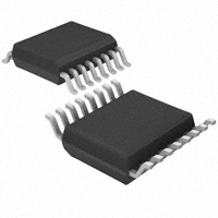
PW PACKAGE (TSSOP)
(TOP VIEW)
Four
D Input Frequency Range: 2.5 MHz to 45 MHz
D Output Frequency Range: 10 MHz to
D
D
D
D
D
D
D
D
D
D
CLKIN
1Y0
1Y1
VDD
GND
2Y0
2Y1
S2
180 MHz
LVCMOS/LVTTL I/O Compatible
Low Jitter (Cycle-Cycle): ±120 ps Over the
Range 75 MHz to 180 MHz
Distributes One Clock Input to Two Banks
of Four Outputs
Auto Frequency Detection to Disable
Device (Power-Down Mode)
Operates From Single 3.3-V Supply
Industrial Temperature Range –40°C to
85°C
25-Ω On-Chip Series Damping Resistors
No External RC Network Required
Spread Spectrum Clock Compatible (SSC)
Available in 16-Pin TSSOP Package
1
2
3
4
5
6
7
8
16
15
14
13
12
11
10
9
FBIN
1Y3
1Y2
VDD
GND
2Y3
2Y2
S1
description
The CDCVF25084 is a high-performance, low-skew, low-jitter, phase-lock loop clock multiplier. It uses a PLL
to precisely align, in both frequency and phase, the output clocks to the input clock signal including a
multiplication factor of four. The CDCVF25084 operates from a nominal supply voltage of 3.3 V. The device also
includes integrated series-damping resistors in the output drivers that make it ideal for driving point-to-point
loads.
Two banks of four outputs each provide low-skew, low-jitter copies of CLKIN x four. All outputs operate at the
same frequency. Output duty cycles are adjusted to 50%, independent of duty cycle at CLKIN. The device
automatically goes into power-down mode when no input signal is applied to CLKIN and the outputs go into a
low state. Unlike many products containing PLLs, the CDCVF25084 does not require an external RC network.
The loop filter for the PLL is included on-chip, minimizing component count, space, and cost.
Because it is based on a PLL circuitry, the CDCVF25084 requires a stabilization time to achieve phase lock of
the feedback signal to the reference signal. This stabilization is required following power up and application of
a fixed-frequency signal at CLKIN and any following changes to the PLL reference.
The CDCVF25084 is characterized for operation from –40°C to 85°C.
FUNCTION TABLE
S2
S1
1Y0–1Y3
2Y0–2Y3
OUTPUT SOURCE
PLL SHUTDOWN
0
0
Hi-Z
Hi-Z
Yes
0
1
Active
Hi-Z
N/A
PLL†
1
0
Active
Active
Input clock (PLL bypass)
PLL†
Yes
1
1
Active
Active
† A CLK input frequency < 2 MHz switches the outputs to low level.
No
No
Please be aware that an important notice concerning availability, standard warranty, and use in critical applications of
Texas Instruments semiconductor products and disclaimers thereto appears at the end of this data sheet.
Copyright 2003, Texas Instruments Incorporated
PRODUCTION DATA information is current as of publication date.
Products conform to specifications per the terms of Texas Instruments
standard warranty. Production processing does not necessarily include
testing of all parameters.
POST OFFICE BOX 655303
• DALLAS, TEXAS 75265
1
�CDCVF25084
3.3-V 1:8 ZERO DELAY (PLL) x4 CLOCK MULTIPLIER
SCAS690A – APRIL 2003 – REVISED MAY 2003
Terminal Functions
TERMINAL
2
TYPE
DESCRIPTION
NAME
PIN NO.
1Y[0:3]
2, 3, 14, 15
O
Bank 1Yn clock outputs. These outputs are low-skew copies of CLKIN. Each output has an integrated
25-Ω series-damping resistor.
2Y[0:3]
6, 7, 10, 11
O
Bank 2Yn clock outputs. These outputs are low-skew copies of CLKIN. Each output has an integrated
25-Ω series-damping resistor.
CLKIN
1
I
Clock input. CLKIN provides the clock signal to be distributed by the CDCVF25084 clock driver. CLKIN is
used to provide the reference signal to the integrated PLL that generates the output signal. CLKIN must
have a fixed frequency and phase in order for the PLL to acquire lock. Once the circuit is powered up and
a valid signal is applied, a stabilization time is required for the PLL to phase lock the feedback signal to
CLKIN.
FBIN
16
I
Feedback input. FBIN provides the feedback signal to the internal PLL. FBIN must be wired to one of the
outputs to complete the feedback loop of the internal PLL. The integrated PLL synchronizes the FBIN and
output signal so there is nominally zero-delay from input clock to output clock.
GND
5, 12
Ground
S1, S2
9, 8
I
VDD
4, 13
Power
Ground
Select pins to determine mode of operation. See the FUNCTION TABLE for mode selection options.
Supply voltage. The supply voltage range is 3 V to 3.6 V
POST OFFICE BOX 655303
• DALLAS, TEXAS 75265
�CDCVF25084
3.3-V 1:8 ZERO DELAY (PLL) x4 CLOCK MULTIPLIER
SCAS690A – APRIL 2003 – REVISED MAY 2003
functional block diagram
2
25 Ω
FBIN
CLKIN
16
1Y0
Div by 4
PLL
1
M
U
X
3
25 Ω
14
25 Ω
15
25 Ω
S2
S1
1Y1
1Y2
1Y3
8
9
Input
Select
Decoding
6
25 Ω
7
25 Ω
10
25 Ω
11
25 Ω
POST OFFICE BOX 655303
• DALLAS, TEXAS 75265
2Y0
2Y1
2Y2
2Y3
3
�CDCVF25084
3.3-V 1:8 ZERO DELAY (PLL) x4 CLOCK MULTIPLIER
SCAS690A – APRIL 2003 – REVISED MAY 2003
absolute maximum ratings over operating free-air temperature (unless otherwise noted)†
Supply voltage range, VDD . . . . . . . . . . . . . . . . . . . . . . . . . . . . . . . . . . . . . . . . . . . . . . . . . . . . . . . . . –0.5 V to 4.6 V
Input voltage range, VI (see Notes 1 and 2) . . . . . . . . . . . . . . . . . . . . . . . . . . . . . . . . . . . . . . . . . . –0.5 V to 4.6 V
Output voltage range, VO (see Notes 1 and 2) . . . . . . . . . . . . . . . . . . . . . . . . . . . . . . . . . . –0.5 V to VDD + 0.5 V
Input clamp current, IIK (VI < 0) . . . . . . . . . . . . . . . . . . . . . . . . . . . . . . . . . . . . . . . . . . . . . . . . . . . . . . . . . . . –50 mA
Output clamp current, IOK (VO < 0) . . . . . . . . . . . . . . . . . . . . . . . . . . . . . . . . . . . . . . . . . . . . . . . . . . . . . . . . –50 mA
Continuous total output current, IO (VO = 0 to VDD) . . . . . . . . . . . . . . . . . . . . . . . . . . . . . . . . . . . . . . . . . . ±50 mA
Package thermal impedance, θJA (see Note 3): PW package . . . . . . . . . . . . . . . . . . . . . . . . . . . . . . . 147°C/W
Storage temperature range, Tstg . . . . . . . . . . . . . . . . . . . . . . . . . . . . . . . . . . . . . . . . . . . . . . . . . . . –65°C to 150°C
† Stresses beyond those listed under “absolute maximum ratings” may cause permanent damage to the device. These are stress ratings only, and
functional operation of the device at these or any other conditions beyond those indicated under “recommended operating conditions” is not
implied. Exposure to absolute-maximum-rated conditions for extended periods may affect device reliability.
NOTES: 1. The input and output negative voltage ratings may be exceeded if the input and output clamp-current ratings are observed.
2. This value is limited to 4.6 V maximum.
3. The package thermal impedance is calculated in accordance with JESD 51.
recommended operating conditions
MIN
Supply voltage, VDD
3
NOM
MAX
3.3
3.6
V
0.8
V
Low level input voltage, VIL
High level input voltage, VIH
2
Input voltage, VI
0
UNIT
V
3.6
V
High-level output current, IOH
–12
mA
Low-level output current, IOL
12
mA
85
°C
Operating free-air temperature, TA
–40
timing requirements over recommended ranges of supply voltage, load and operating free-air
temperature
MIN
Input clock frequency, fCLKIN
Input clock duty cycle
Clock frequency, fclkout
4
CL = 15 pF
POST OFFICE BOX 655303
• DALLAS, TEXAS 75265
MAX
UNIT
2.5
NOM
45
MHz
40%
60%
10
180
MHz
�CDCVF25084
3.3-V 1:8 ZERO DELAY (PLL) x4 CLOCK MULTIPLIER
SCAS690A – APRIL 2003 – REVISED MAY 2003
electrical characteristics over recommended operating free-air temperature range (unless
otherwise noted)
PARAMETER
TEST CONDITIONS
MAX
UNIT
II = –18 mA
–1.2
V
±5
µA
fCLKIN = 0 MHz,
fout = 80 MHz,
VDD = 3.3 V
CL = 15 pF
100
µA
80
mA
Vo = 0 V or VDD,
VI = 0 V or VDD
VDD = 3.6 V
±5
µA
Input voltage
IPD
IDD‡
Power-down current
IOZ
CI
Output 3-state
CI
Input capacitance at S1, S2
CO
Output capacitance
VI = 0 V or VDD
VI = 0 V or VDD
High-level
High
level out
output
ut voltage
VDD = min to max,
VDD = 3 V,
IOH = –100 µA
IOH = –12 mA
VDD = 3 V,
VDD = min to max,
IOH = –6 mA
IOL = 100 µA
VDD = 3 V,
VDD = 3 V,
IOL = 12 mA
IOL = 6 mA
VDD = 3 V,
VDD = 3.3 V,
VO = 1 V
VO = 1.65 V
VDD = 3.6 V,
VDD = 3 V,
VO = 3.135 V
VO = 1.95 V
VDD = 3.3 V,
VDD = 3.6 V,
VO = 1.65 V
VO = 0.4 V
VOH
VOL
IOH
IOL
Input current
Dynamic current
Input capacitance at FBIN, CLKIN
Low-level
Low
level out
output
ut voltage
High-level
High
level out
output
ut current
Low-level output current
TYP†
VDD = 3 V,
VI = 0 V or VDD
VIK
II
MIN
60
4
pF
2.2
pF
3
pF
VDD – 0.2
2.1
V
2.4
0.2
0.8
V
0.55
–24
–30
mA
-15
26
mA
33
14
† All typical values are at respective nominal VDD.
‡ All outputs are switching; for IDD over frequency see Figure 9.
POST OFFICE BOX 655303
• DALLAS, TEXAS 75265
5
�CDCVF25084
3.3-V 1:8 ZERO DELAY (PLL) x4 CLOCK MULTIPLIER
SCAS690A – APRIL 2003 – REVISED MAY 2003
switching characteristics over recommended operating free-air temperature range (unless
otherwise noted)
PARAMETER
TEST CONDITIONS
t(lock)
PLL lock time
t(phoffset)
Phase offset (CLKIN to FBIN), (see
Note 5)
tPLH, tPHL
tsk(o)
tsk(
sk(pp))
fout = 100 MHz
fout = 40 MHz to 75 MHz, Vth = VDD/2
Propagation delay
fout = 75 MHz to 180 MHz, Vth = VDD/2
S2 = High, S1 = Low (PLL bypass mode)
Output skew (Yn to Yn) (see Note 4)
See Figure 3
Part-to-part
P
tt
t skew
k
(low-to-high transition)
MIN
TYP†
MAX
±200
2.3
75
UNIT
µs
2
±100
ps
4.5
ns
150
ps
PLL bypass mode
900
PLL mode, fout = 40 MHz to 75 MHz
350
PLL mode, fout = 75 MHz to 180 MHz
300
ps
s
fout = 40 MHz to 75 MHz
fout = 75 MHz to 180 MHz
±220
ps
Jitter (cycle-to-cycle)
(cycle to cycle)
±120
ps
260
ps
tjit(per)
Period jitter
fout = 40 MHz to 75 MHz
fout = 75 MHz to 180 MHz
140
ps
tjit(θ)
Phase jitter
fout = 75 MHz to 180 MHz, peak-to-peak
(see Note 6)
±110
ps
ps
Output duty cycle
fout = 75 MHz to 180 MHz, RMS (see Note 6)
fout = 10 MHz to 180 MHz
26
odc
tjit(cc)
45%
55%
tsk(p)
Pulse skew
S2 = High, S1 = low (PLL bypass mode)
0.3
ns
tr, tf
Rise / fall time rate
See Figure 4
1
3
V/ns
† All typical values are at respective nominal VDD.
NOTES: 4. The tsk(o) specification is only valid for equal loading of all outputs.
5. Similar waveform at CLKIN and FBIN are required. Output 1Y3 is used as a feedback to FBIN loaded with 11 pF and all other outputs
have 15 pF. For phase displacement between CLKIN and Y-outputs, see Figure 5.
6. Input phase jitter < ±50 ps; output sample size is 20000 cycles.
6
POST OFFICE BOX 655303
• DALLAS, TEXAS 75265
�CDCVF25084
3.3-V 1:8 ZERO DELAY (PLL) x4 CLOCK MULTIPLIER
SCAS690A – APRIL 2003 – REVISED MAY 2003
PARAMETER MEASUREMENT INFORMATION
VDD
1000 Ω
From Output Under Test
CL = 15 pF at f = 10 MHz to 180 MHz
1000 Ω
NOTES: A. CL includes probe and jig capacitance.
B. All input pulses are supplied by generators having the following characteristics: ZO = 50 Ω, tr < 1.2 ns, tf < 1.2 ns
C. The outputs are measured one at a time with one transition per measurement.
Figure 1. Test Load Circuit
VOH
50% VDD
CLKIN
VOL
t(phoffset)
VOH
50% VDD
FBIN
VOL
Figure 2. Voltage Thresholds for Measurements, Phase Offset (PLL Mode)
50% VDD
Any Y
50% VDD
50% VDD
Any Y
t1
tsk(0)
t2
NOTE: odc = t1/(t1 + t2) x 100%
Figure 3. Output Skew and Output Duty Cycle (PLL Mode)
POST OFFICE BOX 655303
• DALLAS, TEXAS 75265
7
�CDCVF25084
3.3-V 1:8 ZERO DELAY (PLL) x4 CLOCK MULTIPLIER
SCAS690A – APRIL 2003 – REVISED MAY 2003
PARAMETER MEASUREMENT INFORMATION
VOH
50% VDD
CLKIN
VOL
tPLH
tPHL
80%
VOH
80%
50% VDD
20%
50% VDD
20%
Any Y
VOL
tr
tf
NOTE: tsk(p)=|tPLH–tPHL|
Figure 4. Propagation Delay and Pulse Skew (Non-PLL Mode)
500
400
300
200
100
0
–100
–200
–300
–400
–500
–600
–700
–800
–900
–1000
–1100
–1200
–1300
–10 –5
PHASE OFFSET
vs
FREQUENCY
250
CL(Yn) = 15 pF,
CL(FBIN) = 11 pF
VCC = 3.3 V,
CYn = 15 pF
t(phoffset) – Phase Offset – ps
Phase Displacement – ps
PHASE DISPLACEMENT
vs
CLOAD
200
150
100
50
0
0
5 10 15 20 25 30 50 35 40 45
–50
10
30
Cload Difference Between FBIN and Yn Pins – pF
(CFBIN + 4 pF) – CYn
70
90
Figure 6
Figure 5
8
50
POST OFFICE BOX 655303
110
130
f – Output Frequency – MHz
• DALLAS, TEXAS 75265
150
170
�CDCVF25084
3.3-V 1:8 ZERO DELAY (PLL) x4 CLOCK MULTIPLIER
SCAS690A – APRIL 2003 – REVISED MAY 2003
PARAMETER MEASUREMENT INFORMATION
CYCLE-TO-CYCLE / PERIOD JITTER
vs
FREQUENCY
TRANSFER CHARACTERISTIC FROM CLKIN TO Yn
20
VDD = 3.3 V
All Outputs
Switching
1200
1100
18
1000
16
900
14
Gain – dB
800
700
600
Cycle-to-Cycle Jitter
500
400
Period Jitter
12
10
8
6
300
4
200
100
0
10
2
30
50
70
90
0
0.1
110 130 150 170 190
f – Output Frequency – MHz
1
10
f – Frequency – MHz
Figure 7
Figure 8
SUPPLY CURRENT
vs
FREQUENCY
180
VDD = 3.6 V
TA = 85°C
160
I DD – Supply Current – mA
t jit(cc) – Cycle-to-Cycle / Period Jitter – ps
1300
VDD = 3 V
TA = –40°C
140
VDD = 3 V
TA = –40°C
120
100
VDD = 3 V
TA = –40°C
80
60
40
20
0
10
30
50 70 90 110 130 150 170 190
f – Output frequency – MHz
Figure 9
POST OFFICE BOX 655303
• DALLAS, TEXAS 75265
9
�PACKAGE OPTION ADDENDUM
www.ti.com
10-Dec-2020
PACKAGING INFORMATION
Orderable Device
Status
(1)
Package Type Package Pins Package
Drawing
Qty
Eco Plan
(2)
Lead finish/
Ball material
MSL Peak Temp
Op Temp (°C)
Device Marking
(3)
(4/5)
(6)
CDCVF25084PW
ACTIVE
TSSOP
PW
16
90
RoHS & Green
NIPDAU
Level-1-260C-UNLIM
-40 to 85
CK084
CDCVF25084PWR
ACTIVE
TSSOP
PW
16
2000
RoHS & Green
NIPDAU
Level-1-260C-UNLIM
-40 to 85
CK084
CDCVF25084PWRG4
ACTIVE
TSSOP
PW
16
2000
RoHS & Green
NIPDAU
Level-1-260C-UNLIM
-40 to 85
CK084
(1)
The marketing status values are defined as follows:
ACTIVE: Product device recommended for new designs.
LIFEBUY: TI has announced that the device will be discontinued, and a lifetime-buy period is in effect.
NRND: Not recommended for new designs. Device is in production to support existing customers, but TI does not recommend using this part in a new design.
PREVIEW: Device has been announced but is not in production. Samples may or may not be available.
OBSOLETE: TI has discontinued the production of the device.
(2)
RoHS: TI defines "RoHS" to mean semiconductor products that are compliant with the current EU RoHS requirements for all 10 RoHS substances, including the requirement that RoHS substance
do not exceed 0.1% by weight in homogeneous materials. Where designed to be soldered at high temperatures, "RoHS" products are suitable for use in specified lead-free processes. TI may
reference these types of products as "Pb-Free".
RoHS Exempt: TI defines "RoHS Exempt" to mean products that contain lead but are compliant with EU RoHS pursuant to a specific EU RoHS exemption.
Green: TI defines "Green" to mean the content of Chlorine (Cl) and Bromine (Br) based flame retardants meet JS709B low halogen requirements of


 工商网监
湘ICP备2023018690号
工商网监
湘ICP备2023018690号
