CDCVF310
www.ti.com
SCAS771B – AUGUST 2004 – REVISED JANUARY 2008
2.5-V TO 3.3-V HIGH-PERFORMANCE CLOCK BUFFER
FEATURES
1
•
•
•
•
•
•
•
•
•
High-Performance 1:10 Clock Driver
Pin-to-Pin Skew < 100 ps at VDD 3.3 V
VDD Range = 2.3 V to 3.6 V
Input Clock Up To 200 MHz (See Figure 7)
Operating Temperature Range –40°C to 85°C
Output Enable Glitch Suppression
Distributes One Clock Input to Two Banks of
Five Outputs
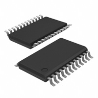
Packaged in 24-Pin TSSOP
Pin-to-Pin Compatible to the CDCVF2310,
Except the R = 22-Ω Series Damping
Resistors at Yn
PW PACKAGE
(TOP VIEW)
GND
VDD
1Y0
1Y1
1Y2
GND
GND
1Y3
1Y4
VDD
1G
2Y4
1
2
3
4
5
6
7
8
9
10
11
12
24
23
22
21
20
19
18
17
16
15
14
13
CLK
VDD
VDD
2Y0
2Y1
GND
GND
2Y2
2Y3
VDD
VDD
2G
APPLICATIONS
•
General-Purpose Applications
DESCRIPTION
The CDCVF310 is a high-performance, low-skew clock buffer that operates up to 200 MHz. Two banks of five
outputs each provide low-skew copies of CLK. After power up, the default state of the outputs is low regardless
of the state of the control pins. For normal operation, the outputs of bank 1Y[0:4] or 2Y[0:4] can be placed in a
low state when the control pins (1G or 2G, respectively) are held low and a negative clock edge is detected on
the CLK input. The outputs of bank 1Y[0:4] or 2Y[0:4] can be switched into the buffer mode when the control pins
(1G and 2G) are held high and a negative clock edge is detected on the CLK input. The device operates in a
2.5-V and 3.3-V environment. The built-in output enable glitch suppression ensures a synchronized output enable
sequence to distribute full period clock signals.
The CDCVF310 is characterized for operation from –40C to 85C.
1
Please be aware that an important notice concerning availability, standard warranty, and use in critical applications of
Texas Instruments semiconductor products and disclaimers thereto appears at the end of this data sheet.
PRODUCTION DATA information is current as of publication date.
Products conform to specifications per the terms of the Texas
Instruments standard warranty. Production processing does not
necessarily include testing of all parameters.
Copyright © 2004–2008, Texas Instruments Incorporated
�CDCVF310
www.ti.com
SCAS771B – AUGUST 2004 – REVISED JANUARY 2008
These devices have limited built-in ESD protection. The leads should be shorted together or the device placed in conductive foam
during storage or handling to prevent electrostatic damage to the MOS gates.
FUNCTIONAL BLOCK DIAGRAM
3
4
5
8
9
1G
2G
11
Logic Control
13
Logic Control
21
CLK
24
20
17
16
12
2
Submit Documentation Feedback
1Y0
1Y1
1Y2
1Y3
1Y4
2Y0
2Y1
2Y2
2Y3
2Y4
Copyright © 2004–2008, Texas Instruments Incorporated
Product Folder Link(s): CDCVF310
�CDCVF310
www.ti.com
SCAS771B – AUGUST 2004 – REVISED JANUARY 2008
FUNCTION TABLE
INPUT
(1)
OUTPUT
1G
2G
CLK
1Y[0:4]
2Y[0:4]
L
L
↓
L
L
(1)
H
L
↓
CLK
L
H
↓
L
CLK (1)
H
H
↓
CLK (1)
CLK (1)
L
After detecting one negative edge on the CLK input, the output
follows the input CLK if the control pin is held high.
Terminal Functions
TERMINAL
NAME
NO.
I/O
DESCRIPTION
1G
11
I
Output enable control for 1Y[0:4] outputs. This output enable is active-high, meaning the
1Y[0:4] clock outputs follow the input clock (CLK) if this pin is logic high.
2G
13
I
Output enable control for 2Y[0:4] outputs. This output enable is active-high, meaning the
2Y[0:4] clock outputs follow the input clock (CLK) if this pin is logic high.
1Y[0:4]
3, 4, 5, 8, 9
O
Buffered output clocks
2Y[0:4]
21, 20, 17, 16, 12
O
Buffered output clocks
CLK
24
I
Input reference frequency
GND
1, 6, 7, 18, 19
VDD
2, 10, 14, 15, 22, 23
Ground
DC power supply, 2.3 V – 3.6 V
Submit Documentation Feedback
Copyright © 2004–2008, Texas Instruments Incorporated
Product Folder Link(s): CDCVF310
3
�CDCVF310
www.ti.com
SCAS771B – AUGUST 2004 – REVISED JANUARY 2008
DETAILED DESCRIPTION
Output Enable Glitch Suppression Circuit
The purpose of the glitch suppression circuitry is to ensure the output enable sequence is synchronized with the
clock input such that the output buffer is enabled or disabled on the next full period of the input clock (negative
edge triggered by the input clock) (see Figure 1).
The G input must fulfill the timing requirements (tsu, th) according to the Switching Characteristics table for
predictable operation.
CLK
Gn
Yn
tsu(en)
th(en)
a) Enable Mode
CLK
Gn
Yn
tsu(dis)
th(dis)
b) Disable Mode
Figure 1. Enable and Disable Mode Relative to CLK↓
4
Submit Documentation Feedback
Copyright © 2004–2008, Texas Instruments Incorporated
Product Folder Link(s): CDCVF310
�CDCVF310
www.ti.com
SCAS771B – AUGUST 2004 – REVISED JANUARY 2008
ABSOLUTE MAXIMUM RATINGS
over operating free-air temperature range (unless otherwise noted)
(1)
Supply voltage range, VDD
–0.5 V to 4.6 V
Input voltage range, VI (2) (3)
–0.5 V to VDD + 0.5 V
Output voltage range, VO (2) (3)
–0.5 V to VDD + 0.5 V
Input clamp current, IIK (VI < 0 or VI> VDD)
±50 mA
Output clamp current, IOK (VO < 0 or VO > VDD)
±50 mA
Continuous total output current, IO (VO = 0 to VDD)
±50 mA
88°C/W, high K
Package thermal impedance, θJA (4): PW package
120°C/W, low K
Storage temperature range Tstg
(1)
(2)
(3)
(4)
–65°C to 150°C
Stresses beyond those listed under “absolute maximum ratings” may cause permanent damage to the device. These are stress ratings
only, and functional operation of the device at these or any other conditions beyond those indicated under “recommended operating
conditions” is not implied. Exposure to absolute-maximum-rated conditions for extended periods may affect device reliability.
The input and output negative voltage ratings may be exceeded if the input and output clamp-current ratings are observed.
This value is limited to 4.6 V maximum.
The package thermal impedance is calculated in accordance with JESD 51.
RECOMMENDED OPERATING CONDITIONS
(1)
Supply voltage, VDD
Low-level input voltage, VIL
High-level input voltage, VIH
NOM
2.3
2.5
3.3
Low-level output current, IOL
3.6
0.8
VDD = 2.3 V to 2.7 V
0.7
VDD = 3 V to 3.6 V
2
VDD = 2.3 V to 2.7 V
VDD = 3 V to 3.6 V
VDD
–12
VDD = 2.3 V to 2.7 V
–6
VDD = 3 V to 3.6 V
12
VDD = 2.3 V to 2.7 V
6
Operating free-air temperature, TA
UNIT
V
V
V
1.7
0
High-level output current, IOH
MAX
VDD = 3 V to 3.6 V
Input voltage, VI
(1)
MIN
–40
85
V
mA
mA
°C
Unused inputs must be held high or low to prevent them from floating.
TIMING REQUIREMENTS
over operating free-air temperature range (unless otherwise noted)
PARAMETER
fclk
Clock frequency
TEST CONDITIONS
VDD = 2.3 V to 3.6 V, See Figure 7
MIN
0
TYP
MAX
UNIT
200
MHz
Submit Documentation Feedback
Copyright © 2004–2008, Texas Instruments Incorporated
Product Folder Link(s): CDCVF310
5
�CDCVF310
www.ti.com
SCAS771B – AUGUST 2004 – REVISED JANUARY 2008
ELECTRICAL CHARACTERISTICS
over recommended operating free-air temperature range (unless otherwise noted) (1)
PARAMETER
TEST CONDITIONS
MIN
TYP
UNIT
Input voltage
VDD = 3 V,
II
Input current
VI = 0 V or VDD
IDD (2)
Static device current
CLK = 0 V or VDD = 3.6 V,
IO = 0 mA
CI
Input capacitance
VDD = 2.3 V to 3.6 V,
VI = 0 V or VDD
2.5
pF
CO
Output capacitance
VDD = 2.3 V to 3.6 V,
VI = 0 V or VDD
2.6
pF
(3)
VDD = 2.3 V to 3.6 V,
VI= 0 V or VDD
CPD
(1)
(2)
(3)
Power dissipation
II = –18 mA
MAX
VIK
–1.2
V
±5
µA
80
µA
32
pF
All typical values are with respect to nominal VDD.
For dynamic IDD over Frequency see Figure 6.
This is the formula for the power dissipation calculation.
P_tot + P_stat ) P_Dyn ) P_Load[W]
P_stat + V DD
I DD [W]
P_Dyn + C_PD
VDD
VDD
ƒ [W]
P_Load + C_Load VDD VDD
ƒ
n + Number of switching output pins
n [W]
VDD = 3.3 V ±0.3 V
PARAMETER
TEST CONDITIONS
VDD = min to max,
VOH
High-level output voltage
VDD = 3 V
VDD = min to max,
VOL
IOH
IOL
(1)
Low-level output voltage
High-level output current
Low-level output current
VDD = 3 V
MIN
IOH = –100 µA
VDD - 0.2
IOH = –12 mA
2.1
IOH = –6 mA
2.4
TYP (1) MAX
V
IOL = 100 µA
0.2
IOL = 12 mA
0.4
IOL = 6 mA
0.3
VDD = 3 V,
VO = 1 V
VDD = 3.3 V,
VO = 1.65 V
VDD = 3.6 V,
VO = 3.135 V
VDD = 3 V,
VO = 1.95 V
VDD = 3.3 V,
VO = 1.65 V
VDD = 3.6 V,
VO = 0.4 V
UNIT
V
–37
–57
mA
–38
37
57
mA
38
All typical values are with respect to nominal VDD.
VDD = 2.5 V ±0.2 V
PARAMETER
VOH
High-level output voltage
VOL
Low-level output voltage
IOH
High-level output current
IOL
(1)
6
Low-level output current
TEST CONDITIONS
MIN
TYP (1)
MAX
VDD = min to max,
IOH = –100 A
VDD - 0.2
VDD = 2.3 V
IOH = –6 mA
1.8
VDD = min to max,
IOL = 100 A
0.2
VDD = 2.3 V
IOL = 6 mA
0.4
VDD = 2.3 V,
VO = 1 V
VDD = 2.5 V,
VO = 1.25 V
VDD = 2.7 V,
VO = 2.375 V
VDD = 2.3 V,
VO = 1.2 V
VDD = 2.5 V,
VO = 1.25 V
VDD = 2.7 V,
VO = 0.3 V
UNIT
V
V
–20
–36
mA
–25
20
36
mA
25
All typical values are with respect to nominal VDD.
Submit Documentation Feedback
Copyright © 2004–2008, Texas Instruments Incorporated
Product Folder Link(s): CDCVF310
�CDCVF310
www.ti.com
SCAS771B – AUGUST 2004 – REVISED JANUARY 2008
JITTER CHARACTERISTICS
Characterized using CDCVF310 Performance EVM when VDD=3.3 V. Outputs not under test are terminated to 50 Ω.
PARAMETER
tjitter
TEST CONDITIONS
Additive phase jitter from input to output 1Y0
MIN
TYP
12 kHz to 5 MHz, fout = 30.72 MHz
47
12 kHz to 20 MHz, fout = 125 MHz
40
MAX
UNIT
fs rms
SWITCHING CHARACTERISTICS
over recommended operating free-air temperature range (unless otherwise noted)
PARAMETER
TEST CONDITIONS
MIN
TYP (1)
MAX
UNIT
VDD = 3.3 V ±0.3 V (see Figure 2)
tPLH
CLK to Yn
tPHL
f = 0 MHz to 200 MHz
(2)
1
2.8
1
2.8
(see Figure 4)
100
ns
tsk(o)
Output skew (Ym to Yn)
tsk(p)
Pulse skew (see Figure 5)
150
ps
250
ps
tsk(pp)
Part-to-part skew
350
ps
tr
Rise time
VO = 0.4 V to 2 V
1.3
2.7
V/ns
tf
Fall time
VO = 2 V to 0.4 V
1.3
2.7
V/ns
tsu(en)
Enable setup time, G_high before CLK ↓
0.1
ns
tsu(dis)
Disable setup time, G_low before CLK ↓
0.1
ns
th(en)
Enable hold time, G_high after CLK ↓
0.4
ns
th(dis)
Disable hold time, G_low after CLK ↓
0.4
ns
VDD = 2.5 V ±0.2 V (see Figure 2)
tPLH
CLK to Yn
tPHL
f = 0 MHz to 200 MHz
(2)
1.3
4
1.3
4
tsk(o)
Output skew (Ym to Yn)
230
ps
tsk(p)
Pulse skew (see Figure 5)
280
ps
tsk(pp)
Part-to-part skew
400
ps
tr
Rise time
VO = 0.4 V to 1.7 V
0.5
1.6
V/ns
tf
Fall time
VO = 1.7 V to 0.4 V
0.5
1.6
V/ns
tsu(en)
Enable setup time, G_high before CLK ↓
0.1
ns
tsu(dis)
Disable setup time, G_low before CLK ↓
0.1
ns
th(en)
Enable hold time, G_high after CLK ↓
0.4
ns
th(dis)
Disable hold time, G_low after CLK ↓
0.4
ns
(1)
(2)
(see Figure 4 )
150
ns
All typical values are with respect to nominal VDD.
The tsk(o) specification is only valid for equal loading of all outputs.
Submit Documentation Feedback
Copyright © 2004–2008, Texas Instruments Incorporated
Product Folder Link(s): CDCVF310
7
�CDCVF310
www.ti.com
SCAS771B – AUGUST 2004 – REVISED JANUARY 2008
PARAMETER MEASUREMENT INFORMATION
From Output
Under Test
500 Ω
CL = 25 pF on Yn
A.
CL includes probe and jig capacitance.
B.
All input pulses are supplied by generators having the following characteristics: Clock Frequency ≤ 200 MHz, ZO = 50
Ω,
tr < 1.2 ns, tf < 1.2 ns.
Figure 2. Test Load Circuit
VDD
50% VDD
0V
CLK
tPLH
tPHL
1.7 V or 2 V
Yn
0.4 V
0.4 V
tr
VOH
50% VDD
VOL
tf
Figure 3. Voltage Waveforms Propagation Delay Times
VDD
CLK
0V
VOH
50% VDD
Any Y
VOL
VOH
50% VDD
Any Y
VOL
tsk(o)
tsk(o)
Figure 4. Output Skew
VDD
50% VDD
CLK
0V
tPLH
tPHL
VOH
Yn
50% VDD
VOL
NOTE: tsk(p) = | tPLH − tPHL |
Figure 5. Pulse Skew
8
Submit Documentation Feedback
Copyright © 2004–2008, Texas Instruments Incorporated
Product Folder Link(s): CDCVF310
�CDCVF310
www.ti.com
SCAS771B – AUGUST 2004 – REVISED JANUARY 2008
DYNAMIC SUPPLY CURRENT
vs
CLOCK FREQUENCY
50
VDD = 2.3 V to 3.6 V
CL(Yn) = No Load
CPD = 32 pF
CO = 10 x 2.6 pF
CI = 3 x 2.5 pF
All Outputs Switching
TA = -405C to 855C
Dynamic Supply Current - mA
45
40
35
30
25
VDD = 3.3 V, No C_Load, TA = 255C
VDD = 3.6 V, No C_Load, TA = -405C
20
15
VDD = 2.7 V, No C_Load, TA = -405C
10
VDD = 2.5 V, No C_Load, TA = 255C
5
0
0
20
40
60
80
100
120
140
160
180
200
fCLK - Clock Frequency - MHz
Figure 6.
C_LOAD(max) PER OUTPUT PIN Yn
vs
CLOCK FREQUENCY
40
VDD = 2.7 V, TA = -405C
for High-K Material
35
C_Load - pF
30
25
20
VDD = 3.6 V, TA = -405C
for High-K Material
15
VDD = 2.3 V to 3.6 V
CL(Yn) max = According to Graph
CPD = 32 pF
CO = 10 x 2.6 pF
CI = 3 x 2.5 pF
All Outputs Switching
TA = -405C to 855C
10
5
0
0
20
40
60
80
100
120
140
160
180
200
fCLK - Clock Frequency - MHz
Figure 7.
Submit Documentation Feedback
Copyright © 2004–2008, Texas Instruments Incorporated
Product Folder Link(s): CDCVF310
9
�PACKAGE OPTION ADDENDUM
www.ti.com
10-Dec-2020
PACKAGING INFORMATION
Orderable Device
Status
(1)
Package Type Package Pins Package
Drawing
Qty
Eco Plan
(2)
Lead finish/
Ball material
MSL Peak Temp
Op Temp (°C)
Device Marking
(3)
(4/5)
(6)
CDCVF310PW
ACTIVE
TSSOP
PW
24
60
RoHS & Green
NIPDAU
Level-1-260C-UNLIM
-40 to 85
CKV310
CDCVF310PWR
ACTIVE
TSSOP
PW
24
2000
RoHS & Green
NIPDAU
Level-1-260C-UNLIM
-40 to 85
CKV310
(1)
The marketing status values are defined as follows:
ACTIVE: Product device recommended for new designs.
LIFEBUY: TI has announced that the device will be discontinued, and a lifetime-buy period is in effect.
NRND: Not recommended for new designs. Device is in production to support existing customers, but TI does not recommend using this part in a new design.
PREVIEW: Device has been announced but is not in production. Samples may or may not be available.
OBSOLETE: TI has discontinued the production of the device.
(2)
RoHS: TI defines "RoHS" to mean semiconductor products that are compliant with the current EU RoHS requirements for all 10 RoHS substances, including the requirement that RoHS substance
do not exceed 0.1% by weight in homogeneous materials. Where designed to be soldered at high temperatures, "RoHS" products are suitable for use in specified lead-free processes. TI may
reference these types of products as "Pb-Free".
RoHS Exempt: TI defines "RoHS Exempt" to mean products that contain lead but are compliant with EU RoHS pursuant to a specific EU RoHS exemption.
Green: TI defines "Green" to mean the content of Chlorine (Cl) and Bromine (Br) based flame retardants meet JS709B low halogen requirements of