CLC520
Amplifier with Voltage Controlled Gain, AGC +Amp
General Description
Features
The CLC520 is a wideband DC-coupled amplifier with voltage controlled gain (AGC). The amplifier has a high impedance, differential signal input; a high bandwidth, gain control
input; and a single-ended voltage output. Signal channel
performance is outstanding with 160MHz small signal bandwidth, 0.5 degree linear phase deviation (to 60MHz) and
0.04% signal nonlinearity at 4VPP output.
Gain control is very flexible and easy to use. Maximum gain
may be set over a nominal range of 2 to 100 with one
external resistor. In addition, the gain control input provides
more than 40dB of voltage controlled gain adjustment from
the maximum gain setting. For example, a CLC520 may be
set for a maximum gain of 2 (or 6dB) for a voltage controlled
gain range from 40dB to less than 34dB. Alternatively, the
CLC520 could be set for a maximum gain of 100 or (40dB)
for a voltage controlled gain range from 40dB to less than
0dB.
The gain control bandwidth of 100MHz is superb for AGC/
ALC loop stabilization. And since the gain is minimum with a
zero volt input and maximum with a +2 volt input, driving the
control input is easy.
Finally, the CLC520 differential inputs, and ground referenced voltage output take the trouble out of designing
DC-coupled AGC circuits for display normalizers; signal leveling automatic circuits; etc.
Enhanced Solutions (Military/Aerospace)
SMD Number: 5962-91694
Space level versions also available.
For more information, visit http://www.national.com/mil
n
n
n
n
n
n
160MHz, −3dB bandwidth
2000V/µsec slew rate
0.04% signal nonlinearity at 4VPP output
−43dB feedthrough at 30MHz
User adjustable gain range
Differential voltage input and single-ended voltage
output
Applications
n
n
n
n
n
n
Wide bandwidth AGC systems
Automatic signal leveling
Video signal processing
Voltage controlled filters
Differential amplifier
Amplitude modulation
Gain vs. Vg
01275640
Connection Diagram
01275639
Gain vs. Vg
01275629
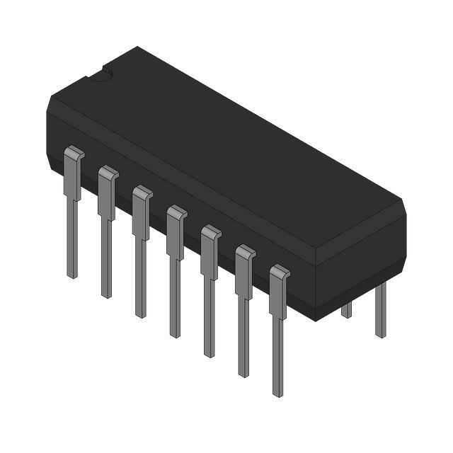
Pinout
DIP & SOIC
© 2001 National Semiconductor Corporation
DS012756
www.national.com
CLC520 Amplifier with Voltage Controlled Gain, AGC +Amp
May 2001
�CLC520
Ordering Information
Package
Temperature Range
Industrial
Part Number
Package
Marking
14-pin plastic DIP
−40˚C to +85˚C
CLC520AJP
CLC520AJP
N14A
14-pin plastic SOIC
−40˚C to +85˚C
CLC520AJE
CLC520AJE
M14A
www.national.com
2
NSC
Drawing
�(Note 1)
Junction Temperature
Operating Temperature Range
If Military/Aerospace specified devices are required,
please contact the National Semiconductor Sales Office/
Distributors for availability and specifications.
10 sec
ESD (human body model)
60mA
Package
Common Mode Input Voltage
± VCC
10V
500V
Operating Ratings
Thermal Resistance
VIN Differential Input Voltage
Vref Differential Input Voltage
−65˚C to +150˚C
Lead Solder Duration (+300˚C)
IOUT
Output is short circuit protected to
ground, but maximum reliability will
be maintained if IOUT does not
exceed...
Vg Differential Input Voltage
−40˚C to +85˚C
Storage Temperature Range
± 7V
Supply Voltage (VCC)
+150˚C
(θJC)
(θJA)
MDIP
55˚C/W
105˚C/W
SOIC
45˚C/W
120˚C/W
± VCC
± VCC
Electrical Characteristics
AV = +10, VCC = ± 5V, RL = 100Ω, Rf = 1kΩ, Rg = 182Ω, Vg = +2V; unless specified
Symbol
Parameter
Ambient Temperature
Conditions
CLC520AJ
Typ
Max/Min (Note 2)
Units
+25˚C
−40˚C
+25˚C
+85˚C
> 120
> 100
> 100
> 120
> 100
> 100
MHz
Frequency Domain Response
SSBW
-3dB Bandwidth
VOUT < 0.5VPP
160
140
> 110
> 90
> 85
-3dB Bandwidth
VOUT < 0.5VPP (AJE only)
VOUT < 4.0VPP
VOUT < 0.5VPP
Gain Control Channel
VIN = +0.2V, Vg = +1VDC
100
> 80
> 80
> 80
MHz
< 0.3
< 0.5
< 0.3
±2
mV
750
> 535
±3
> ± 35
> 600
± 3.2
> ± 50
> 600
± 3.2
> ± 50
Ω
12
DIB
Average Temperature Doefficient
100
IOS
Input Offset Current
0.5
DIOS
Average Temperature Coefficient
PSS
Power Supply Sensitivity
Output Referred DC
10
CMRR
Common Mode Rejection Ratio
Input Referred
70
ICC
Supply Current (Note 5)
No Load
28
RIN
VIN Signal Input
Resistance
200
Capacitance
DMIR
VIN Differential Voltage Range
CMIR
Common Mode Voltage Range
RINC
Vg Control Input
CINC
VGHI
5
Rg = 182Ω only
Resistance
Capacitance
Vg Input Voltage
VGLO
1
For Max Gain
1.6
For Min Gain
0.4
0.1
RO
Output Impedance
At DC
VO
Output Voltage Range
No Load
IO
Output Current
± 3.5
± 60
< 28
Units
< 28
< 165
59
< 38
> 100
50
740 ˚ Vdmax −3Ω
Operating with Rg larger than this value insures linear operation of the input buffers.
Rf may be computed from selected Rg and AVMAX:
01275648
FIGURE 5. Equivalent Input Noise Voltage (en) vs. Rg
Several points should be made concerning this model. First,
external component noise contributions need to be factored
in when computing total output referred noise. The only
exception is Rg, where its noise contribution is already factored in. Second, the model ignores flicker noise contributions. Applications where noise below approximately 100kHz
must be considered should use this model with caution.
Third, this model very accurately predicts output noise voltage for the typical application circuit (see above) but accuracy will degrade the component values deviate further from
those in the typical application circuit. In general, however,
Rf should be > = 1kΩ for overall best performance, however
Rf < 1kΩ can be implemented if necessary using a loop gain
reducing resistor to ground on the inverting summing node of
the output amplifier (see application note QA-13 for details).
Printed Circuit Layout
A good high frequency PCB layout including ground plane
construction and power supply bypassing close to the package are critical to achieving full performance. The amplifier is
sensitive to stray capacitance to ground at the
Inverting-input (pin12); keep node trace area small. Shunt
www.national.com
10
�CLC520
Application Information
(Continued)
the model should predict the equivalent output noise above
the flicker noise region to within a few dB of actual performance over the normal range of AVMAX and component
values.
ino does not contribute to the output buffer noise because the
output buffer non-inverting input is grounded.
The core noise is already output referred and is 37nV/
at Vg =1.1 (AVMAX/2) and approaches zero as A goes to 0 or
AVMAX Summing the noise power for each term gives the
total output noise power.
The total output noise voltage is given by:
01275610
FIGURE 6. Typical Circuit
Where AV is the input to output voltage gain, which varies
with Vg.
C accounts for the variation in core noise contribution as Vg
is adjusted. C=1 when gain AV is AVMAX/2. C is zero at
AVMAX and AV = 0 and varies between 0 and 1 for all other
values.
Using these equations, total calculated output noise for the
circuit was 20nV/
at minimum gain, 49nV/
at
mid-gain, and 53nV/
at maximum gain.
01275611
FIGURE 7. Noise Model for Typical Circuit
Calculating CLC520 output noise in a typical circuit
To calculate the noise in a CLC520 application, the noise
terms given for the amplifier as well as the noise terms of the
external components must be included. To clarify the techniques used, output noise in a typical circuit will be calculated. (Figure 6)
The noise model is depicted in Figure 7. The diagram assumes spot noise source with Vrms/
and Ampsrms/
units. The Thevenin equivalent of the source and input termination is used; 25Ω in series with a noise voltage source.
Rg is assumed noiseless since its effect is included in en.
The internal 5kΩ resistor at the CLC520 core output is also
assumed noiseless since its effect is included in iio, The
noise contribution from Rf is modeled as a noise source.
The easiest way to analyze the output noise of this circuit is
to divide the noise power into three pieces; −input buffer
noise calculation, output buffer noise and core noise. The
input buffer varies with the gain. The output buffer term is
constant. The core noise term is zero at both maximum and
minimum gain and reaches peak at AVMAX/2.
Since we assume all noise terms are uncorrelated, the
equivalent input noise voltage squared is given by:
01275612
FIGURE 8. Automatic Gain Control (AGC) Loop
AGC circuits
Figure 8 shows a typical AGC circuit. The CLC520 is followed up with a CLC401 for higher overall gain. The output
of the CLC401 is rectified and fed to an inverting integrator
using a CLC420 (wideband voltage feedback op amp).
When the output voltage, VOUT, is too large the integrator
output voltage ramps down reducing the net gain of the
CLC520 and VOUT. If the output voltage is too small, the
integrator ramps up increasing the net gain and the output
voltage. Actual output level is set with R1. To prevent shifts in
DC output voltage with DC changes in input signal level, trim
pot R2 is provided. AGC circuits are always limited in the
range of input signals over which constant output level can
be maintained. In this circuit, we would expect that reasonable AGC action could be maintained over the gain adjustment range of the CLC520 (at least 40dB). In practice,
rectifier dynamic range limits reduce this slightly.
Evaluation Board
Evaluation PC boards (part number 730029 for through-hole
and 730023 for SOIC) for the CLC520 are available.
ii does not contribute to the output buffer noise because the
input buffer inverting input is grounded. en is taken from
Figure 5.
The equivalent output buffer noise is given by:
11
www.national.com
�CLC520
Physical Dimensions
inches (millimeters)
unless otherwise noted
14-Pin MDIP
NS Package Number N14A
14-Pin SOIC
NS Package Number M14A
www.national.com
12
�CLC520 Amplifier with Voltage Controlled Gain, AGC +Amp
Notes
LIFE SUPPORT POLICY
NATIONAL’S PRODUCTS ARE NOT AUTHORIZED FOR USE AS CRITICAL COMPONENTS IN LIFE SUPPORT
DEVICES OR SYSTEMS WITHOUT THE EXPRESS WRITTEN APPROVAL OF THE PRESIDENT AND GENERAL
COUNSEL OF NATIONAL SEMICONDUCTOR CORPORATION. As used herein:
1. Life support devices or systems are devices or
systems which, (a) are intended for surgical implant
into the body, or (b) support or sustain life, and
whose failure to perform when properly used in
accordance with instructions for use provided in the
labeling, can be reasonably expected to result in a
significant injury to the user.
National Semiconductor
Corporation
Americas
Email: support@nsc.com
www.national.com
National Semiconductor
Europe
Fax: +49 (0) 180-530 85 86
Email: europe.support@nsc.com
Deutsch Tel: +49 (0) 69 9508 6208
English Tel: +44 (0) 870 24 0 2171
Français Tel: +33 (0) 1 41 91 8790
2. A critical component is any component of a life
support device or system whose failure to perform
can be reasonably expected to cause the failure of
the life support device or system, or to affect its
safety or effectiveness.
National Semiconductor
Asia Pacific Customer
Response Group
Tel: 65-2544466
Fax: 65-2504466
Email: ap.support@nsc.com
National Semiconductor
Japan Ltd.
Tel: 81-3-5639-7560
Fax: 81-3-5639-7507
National does not assume any responsibility for use of any circuitry described, no circuit patent licenses are implied and National reserves the right at any time without notice to change said circuitry and specifications.
�