CSD13303W1015
www.ti.com
SLPS298A – MAY 2012 – REVISED MAY 2012
N-Channel NexFET™ Power MOSFET
Check for Samples: CSD13303W1015
FEATURES
1
•
•
•
•
•
•
•
•
PRODUCT SUMMARY
Ultra Low on Resistance
Ultra Low Qg and Qgd
Small Footprint
Low Profile 0.62 mm Height
Pb Free
RoHS Compliant
Halogen Free
CSP 1 × 1.5 mm Wafer Level Package
TA = 25°C unless otherwise stated
UNIT
Drain to Source Voltage
12
V
Qg
Gate Charge Total (4.5V)
3.9
nC
Qgd
Gate Charge Gate to Drain
RDS(on)
Drain to Source On Resistance
VGS(th)
Voltage Threshold
0.4
nC
VGS = 2.5V
18
mΩ
VGS = 4.5V
16
mΩ
0.85
V
ORDERING INFORMATION
Device
Package
Media
Qty
Ship
CSD13303W1015
1 × 1.5 Wafer
Level Package
7-inch reel
3000
Tape and
Reel
APPLICATIONS
•
•
•
TYPICAL VALUE
VDS
Battery Management
Load Switch
Battery Protection
ABSOLUTE MAXIMUM RATINGS
TA = 25°C unless otherwise stated
DESCRIPTION
The device has been designed to deliver the lowest
on resistance and gate charge in the smallest outline
possible with excellent thermal characteristics in an
ultra low profile.
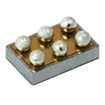
Top View
VALUE
UNIT
VDS
Drain to Source Voltage
12
V
VGS
Gate to Source Voltage
±8
V
ID
Continuous Drain Current, TC = 25°C(1)
3.5
A
IDM
Pulsed Drain Current, TA = 25°C(2)
31
A
PD
Power Dissipation(1)
1.65
W
TSTG
Storage Temperature Range
TJ
Operating Junction Temperature Range
–55 to 150
°C
(1) Typical RθJA = 75.7°C/W on 1in2 Cu (2 oz.) on 0.060" thick
FR4 PCB.
(2) Pulse width ≤1ms, duty cycle ≤2%
RDS(ON) vs VGS
Gate Charge
6
TC = 25°C Id = 1.5A
TC = 125ºC Id = 1.5A
TC = 25ºC Id = 3.5A
TC = 125ºC Id = 3.5A
45
40
35
VGS - Gate-to-Source Voltage (V)
RDS(on) - On-State Resistance - mΩ
50
30
25
20
15
10
5
0
0
1
2
3
4
5
6
VGS - Gate-to- Source Voltage - V
7
8
G001
ID = 3.5A
VDS = 10V
5
4
3
2
1
0
0
1
2
3
Qg - Gate Charge - nC (nC)
4
5
G001
1
Please be aware that an important notice concerning availability, standard warranty, and use in critical applications of
Texas Instruments semiconductor products and disclaimers thereto appears at the end of this data sheet.
PRODUCTION DATA information is current as of publication date.
Products conform to specifications per the terms of the Texas
Instruments standard warranty. Production processing does not
necessarily include testing of all parameters.
Copyright © 2012, Texas Instruments Incorporated
�CSD13303W1015
SLPS298A – MAY 2012 – REVISED MAY 2012
www.ti.com
These devices have limited built-in ESD protection. The leads should be shorted together or the device placed in conductive foam
during storage or handling to prevent electrostatic damage to the MOS gates.
ELECTRICAL CHARACTERISTICS
(TA = 25°C unless otherwise stated)
PARAMETER
TEST CONDITIONS
MIN
TYP
MAX
UNIT
Static Characteristics
BVDSS
Drain to Source Voltage
VGS = 0V, ID = 250μA
IDSS
Drain to Source Leakage Current
VGS = 0V, VDS = 9.6V
IGSS
Gate to Source Leakage Current
VDS = 0V, VGS = +8V
VGS(th)
Gate to Source Threshold Voltage
VDS = VGS, ID = 250μA
RDS(on)
Drain to Source On Resistance
gfs
Transconductance
12
0.65
V
1
μA
100
nA
0.85
1.2
V
VGS = 2.5V, ID = 1.5A
18
23
mΩ
VGS = 4.5V, ID = 1.5A
16
20
mΩ
VDS = 6V, ID =1.5A
14
S
Dynamic Characteristics
CISS
Input Capacitance
COSS
Output Capacitance
CRSS
Reverse Transfer Capacitance
VGS = 0V, VDS = 6V, f = 1MHz
Rg
550
715
pF
400
480
pF
29
36
pF
3
4.6
Ω
4.7
nC
Qg
Gate Charge Total (4.5V)
3.9
Qgd
Gate Charge Gate to Drain
0.4
nC
Qgs
Gate Charge Gate to Source
1
nC
Qg(th)
Gate Charge at Vth
0.6
nC
QOSS
Output Charge
4.9
nC
td(on)
Turn On Delay Time
4.6
ns
tr
Rise Time
10
ns
td(off)
Turn Off Delay Time
14.7
ns
tf
Fall Time
3.2
ns
VDS = 6V, ID = 1.5A
VDS = 6V, VGS = 0V
VDS = 6V, VGS = 4.5V, ID = 1.5A
RG = 4Ω
Diode Characteristics
VSD
Diode Forward Voltage
Qrr
Reverse Recovery Charge
trr
Reverse Recovery Time
IS = 1.5A, VGS = 0V
0.7
VDS= 6V, IF = 1.5A, di/dt = 200A/μs
1
V
14
nC
38.7
ns
THERMAL CHARACTERISTICS
(TA = 25°C unless otherwise stated)
PARAMETER
R θJA
2
Thermal Resistance Junction to Ambient (Minimum Cu area)
Thermal Resistance Junction to Ambient (1 in2 Cu area)
Submit Documentation Feedback
MIN
TYP
MAX
UNIT
295.5
°C/W
94.6
°C/W
Copyright © 2012, Texas Instruments Incorporated
�CSD13303W1015
www.ti.com
SLPS298A – MAY 2012 – REVISED MAY 2012
Max RθJA = 94.6°C/W
when mounted on 1
inch2 of 2 oz. Cu.
Max RθJA = 295.5°C/W
when mounted on
minimum pad area of 2
oz. Cu.
TYPICAL MOSFET CHARACTERISTICS
(TA = 25°C unless otherwise stated)
Figure 1. Transient Thermal Impedance
Copyright © 2012, Texas Instruments Incorporated
Submit Documentation Feedback
3
�CSD13303W1015
SLPS298A – MAY 2012 – REVISED MAY 2012
www.ti.com
TYPICAL MOSFET CHARACTERISTICS (continued)
(TA = 25°C unless otherwise stated)
50
20
IDS - Drain-to-Source Current - A
IDS - Drain-to-Source Current - A
VDS = 5V
40
30
20
VGS =4.5V
VGS =3.5V
VGS =3V
10
0
0
0.1
0.2 0.3 0.4 0.5 0.6 0.7 0.8
VDS - Drain-to-Source Voltage - V
0.9
16
12
8
TC = 125°C
TC = 25°C
TC = −55°C
4
0
0.75
1
Figure 2. Saturation Characteristics
G001
Ciss = Cgd + Cgs
Coss = Cds + Cgd
Crss = Cgd
C − Capacitance − nF
0.9
4
3
2
0.8
0.7
0.6
0.5
0.4
0.3
0.2
1
0.1
0
1
2
3
Qg - Gate Charge - nC (nC)
4
0
5
0
2
G001
Figure 4. Gate Charge
4
6
8
10
VDS - Drain-to-Source Voltage - V
12
G001
Figure 5. Capacitance
1.4
50
RDS(on) - On-State Resistance - mΩ
ID = 250uA
VGS(th) - Threshold Voltage - V
2
1
ID = 3.5A
VDS = 10V
5
0
1.2
1
0.8
0.6
0.4
0.2
0
−75
−25
25
75
125
TC - Case Temperature - ºC
Figure 6. Threshold Voltage vs. Temperature
4
1.25
1.5
1.75
VGS - Gate-to-Source Voltage - V
Figure 3. Transfer Characteristics
6
VGS - Gate-to-Source Voltage (V)
1
G001
Submit Documentation Feedback
175
G001
TC = 25°C Id = 1.5A
TC = 125ºC Id = 1.5A
TC = 25ºC Id = 3.5A
TC = 125ºC Id = 3.5A
45
40
35
30
25
20
15
10
5
0
0
1
2
3
4
5
6
VGS - Gate-to- Source Voltage - V
7
8
G001
Figure 7. On Resistance vs. Gate Voltage
Copyright © 2012, Texas Instruments Incorporated
�CSD13303W1015
www.ti.com
SLPS298A – MAY 2012 – REVISED MAY 2012
TYPICAL MOSFET CHARACTERISTICS (continued)
(TA = 25°C unless otherwise stated)
1.4
10
VGS = 2.5V
VGS = 4.5V
ID = 1.5A
ISD − Source-to-Drain Current - A
Normalized On-State Resistance
1.6
1.2
1
0.8
0.6
0.4
−75
−25
25
75
125
TC - Case Temperature - ºC
175
TC = 25°C
TC = 125°C
1
0.1
0.01
0.001
0.0001
0
0.2
0.4
0.6
0.8
VSD − Source-to-Drain Voltage - V
G001
Figure 8. Normalized On Resistance vs. Temperature
1
G001
Figure 9. Typical Diode Forward Voltage
− IDS - Drain- to- Source Current - A
4.0
3.5
3.0
2.5
2.0
1.5
1.0
0.5
0.0
−50
Figure 10. Maximum Safe Operating Area
−25
0
25
50
75
100 125
TC - Case Temperature - ºC
150
175
G001
Figure 11. Maximum Drain Current vs. Temperature
RDS(on) - On-State Resistance - mΩ
30
28
ID = 3.5A
26
24
22
20
18
16
14
VGS = 2.5V
VGS = 4.5V
12
10
−75
−25
25
75
125
TC - Case Temperature - ºC
175
G001
Figure 12. On Resistance vs. Temperature
Copyright © 2012, Texas Instruments Incorporated
Submit Documentation Feedback
5
�CSD13303W1015
SLPS298A – MAY 2012 – REVISED MAY 2012
www.ti.com
MECHANICAL DATA
CSD13303W1015 Package Dimensions
NOTE: All dimensions are in mm (unless otherwise specified)
Pinout
6
POSITION
DESIGNATION
C2, B2
Source
A2
Gate
A1, B1, C1
Drain
Submit Documentation Feedback
Copyright © 2012, Texas Instruments Incorporated
�CSD13303W1015
www.ti.com
SLPS298A – MAY 2012 – REVISED MAY 2012
Land Pattern Recommendation
Ø 0.25
1
2
1.00
0.50
A
B
C
0.50
M0158-01
NOTE: All dimensions are in mm (unless otherwise specified)
Tape and Reel Information
NOTE: All dimensions are in mm (unless otherwise specified)
Copyright © 2012, Texas Instruments Incorporated
Submit Documentation Feedback
7
�CSD13303W1015
SLPS298A – MAY 2012 – REVISED MAY 2012
www.ti.com
REVISION HISTORY
Changes from Original (May 2012) to Revision A
•
8
Page
Changed the Tape and Reel Information section ................................................................................................................. 7
Submit Documentation Feedback
Copyright © 2012, Texas Instruments Incorporated
�PACKAGE OPTION ADDENDUM
www.ti.com
10-Dec-2020
PACKAGING INFORMATION
Orderable Device
Status
(1)
Package Type Package Pins Package
Drawing
Qty
Eco Plan
(2)
Lead finish/
Ball material
MSL Peak Temp
Op Temp (°C)
Device Marking
(3)
(4/5)
(6)
CSD13303W1015
ACTIVE
DSBGA
YZC
6
3000
RoHS & Green
SNAGCU
Level-1-260C-UNLIM
-55 to 150
13303
(1)
The marketing status values are defined as follows:
ACTIVE: Product device recommended for new designs.
LIFEBUY: TI has announced that the device will be discontinued, and a lifetime-buy period is in effect.
NRND: Not recommended for new designs. Device is in production to support existing customers, but TI does not recommend using this part in a new design.
PREVIEW: Device has been announced but is not in production. Samples may or may not be available.
OBSOLETE: TI has discontinued the production of the device.
(2)
RoHS: TI defines "RoHS" to mean semiconductor products that are compliant with the current EU RoHS requirements for all 10 RoHS substances, including the requirement that RoHS substance
do not exceed 0.1% by weight in homogeneous materials. Where designed to be soldered at high temperatures, "RoHS" products are suitable for use in specified lead-free processes. TI may
reference these types of products as "Pb-Free".
RoHS Exempt: TI defines "RoHS Exempt" to mean products that contain lead but are compliant with EU RoHS pursuant to a specific EU RoHS exemption.
Green: TI defines "Green" to mean the content of Chlorine (Cl) and Bromine (Br) based flame retardants meet JS709B low halogen requirements of
很抱歉,暂时无法提供与“CSD13303W1015”相匹配的价格&库存,您可以联系我们找货
免费人工找货- 国内价格 香港价格
- 1+6.889331+0.89241
- 10+4.2927510+0.55606
- 100+2.76471100+0.35813
- 500+2.10414500+0.27256
- 1000+1.891101000+0.24497