CSD16342Q5A
www.ti.com
SLPS369A – FEBRUARY 2012 – REVISED MARCH 2012
N-Channel NexFET™ Power MOSFETs
Check for Samples: CSD16342Q5A
FEATURES
1
•
•
•
•
•
•
•
•
•
2
PRODUCT SUMMARY
Optimized for 5V Gate Drive
Resistance Rated at VGS = 2.5V
Ultra Low Qg and Qgd
Low Thermal Resistance
Avalanche Rated
Pb Free Terminal Plating
RoHS Compliant
Halogen Free
SON 5mm x 6mm Plastic Package
•
Drain to Source Voltage
25
V
Qg
Gate Charge Total (4.5V)
6.8
nC
Qgd
Gate Charge Gate to Drain
RDS(on)
Top View
S
2
7
D
S
3
6
D
VGS = 4.5V
4.3
mΩ
VGS = 8V
3.8
mΩ
Threshold Voltage
0.85
V
Package
Media
Qty
Ship
CSD16342Q5A
SON 5 × 6 Plastic
Package
13-inch
reel
2500
Tape and
Reel
ABSOLUTE MAXIMUM RATINGS
The NexFET™ power MOSFET has been designed
to minimize losses in power conversion and optimized
for 5V gate drive applications.
D
mΩ
TA = 25°C unless otherwise stated
DESCRIPTION
8
6.1
Device
VALUE
UNIT
VDS
Drain to Source Voltage
25
V
VGS
Gate to Source Voltage
+10 / –8
V
Continuous Drain Current, TC = 25°C
100
A
Continuous Drain Current(1)
21
A
IDM
Pulsed Drain Current, TA = 25°C(2)
131
A
PD
Power Dissipation(1)
3
W
TJ,
TSTG
Operating Junction and Storage
Temperature Range
–55 to 150
°C
EAS
Avalanche Energy, single pulse
ID = 40A, L = 0.1mH, RG = 25Ω
80
mJ
ID
1
nC
VGS = 2.5V
ORDERING INFORMATION
Point-of-Load Synchronous Buck Converter
for Applications in Networking, Telecom and
Computing Systems
Optimized for Control or Synchronous FET
Applications
S
1.2
Drain to Source On Resistance
Vth
APPLICATIONS
•
VDS
(1) Typical RθJA = 40°C/W on 1in2 Cu (2 oz.) on 0.060" thick FR4
PCB.
(2) Pulse width ≤300μs, duty cycle ≤2%
D
G
5
4
D
P0095-01
RDS(ON) vs VGS
Gate Charge
10
ID = 20A
18
VGS - Gate-to-Source Voltage (V)
RDS(on) - On-State Resistance - mΩ
20
16
14
12
10
8
6
4
TC = 25°C
TC = 125ºC
2
0
0
1
2
3
4
5
6
7
VGS - Gate-to- Source Voltage - V
8
9
10
G001
ID =20A
VDD = 12.5V
9
8
7
6
5
4
3
2
1
0
0
2
4
6
8
Qg - Gate Charge - nC (nC)
10
12
G001
1
2
Please be aware that an important notice concerning availability, standard warranty, and use in critical applications of
Texas Instruments semiconductor products and disclaimers thereto appears at the end of this data sheet.
NexFET is a trademark of Texas Instruments.
PRODUCTION DATA information is current as of publication date.
Products conform to specifications per the terms of the Texas
Instruments standard warranty. Production processing does not
necessarily include testing of all parameters.
Copyright © 2012, Texas Instruments Incorporated
�CSD16342Q5A
SLPS369A – FEBRUARY 2012 – REVISED MARCH 2012
www.ti.com
These devices have limited built-in ESD protection. The leads should be shorted together or the device placed in conductive foam
during storage or handling to prevent electrostatic damage to the MOS gates.
ELECTRICAL CHARACTERISTICS
(TA = 25°C unless otherwise stated)
PARAMETER
TEST CONDITIONS
MIN
TYP
MAX
UNIT
Static Characteristics
BVDSS
Drain to Source Voltage
VGS = 0V, IDS = 250μA
IDSS
Drain to Source Leakage Current
VGS = 0V, VDS = 20V
IGSS
Gate to Source Leakage Current
VDS = 0V, VGS = +10/-8V
VGS(th)
Gate to Source Threshold Voltage
VDS = VGS, IDS = 250μA
RDS(on)
gfs
Drain to Source On Resistance
Transconductance
25
0.6
V
1
μA
100
nA
0.85
1.1
V
VGS = 2.5V, IDS = 20A
6.1
7.8
mΩ
VGS = 4.5V, IDS = 20A
4.3
5.5
mΩ
VGS = 8V, IDS = 20A
3.8
4.7
mΩ
VDS = 15V, IDS = 20A
91
S
Dynamic Characteristics
CISS
Input Capacitance
COSS
Output Capacitance
1050
1350
pF
730
950
CRSS
pF
Reverse Transfer Capacitance
53
69
pF
Rg
Series Gate Resistance
1.5
3
Ω
Qg
Gate Charge Total (4.5V)
6.8
7.1
nC
Qgd
Gate Charge Gate to Drain
Qgs
Gate Charge Gate to Source
Qg(th)
Gate Charge at Vth
QOSS
Output Charge
td(on)
Turn On Delay Time
tr
Rise Time
td(off)
Turn Off Delay Time
tf
Fall Time
VGS = 0V, VDS = 12.5V, f = 1MHz
VDS = 12.5V, ID = 20A
VDS = 13V, VGS = 0V
VDS = 12.5V, VGS = 4.5V ID = 20A
RG = 2Ω
0.9
nC
1.9
nC
1.2
nC
13.7
nC
5.2
ns
16.6
ns
13.4
ns
3.1
ns
Diode Characteristics
VSD
Diode Forward Voltage
Qrr
Reverse Recovery Charge
trr
Reverse Recovery Time
IS = 20A, VGS = 0V
0.8
VDD = 13V, IF = 20A, di/dt = 300A/μs
1
V
14.5
nC
20
ns
THERMAL CHARACTERISTICS
(TA = 25°C unless otherwise stated)
PARAMETER
RθJC
RθJA
(1)
(2)
2
Thermal Resistance Junction to Case (1)
Thermal Resistance Junction to Ambient
(1) (2)
MIN
TYP
MAX
UNIT
1.2
°C/W
50
°C/W
RθJC is determined with the device mounted on a 1-inch2 (6.45-cm2), 2-oz. (0.071-mm thick) Cu pad on a 1.5-inch × 1.5-inch (3.81-cm ×
3.81-cm), 0.06-inch (1.52-mm) thick FR4 PCB. RθJC is specified by design, whereas RθJA is determined by the user’s board design.
Device mounted on FR4 material with 1-inch2 (6.45-cm2), 2-oz. (0.071-mm thick) Cu.
Submit Documentation Feedback
Copyright © 2012, Texas Instruments Incorporated
Product Folder Link(s): CSD16342Q5A
�CSD16342Q5A
www.ti.com
GATE
SLPS369A – FEBRUARY 2012 – REVISED MARCH 2012
GATE
Source
Source
Max RθJA = 123°C/W
when mounted on
minimum pad area of 2
oz. Cu.
Max RθJA = 50°C/W
when mounted on 1
inch2 of 2 oz. Cu.
DRAIN
DRAIN
M0161-02
M0161-01
TYPICAL MOSFET CHARACTERISTICS
(TA = 25°C unless otherwise stated)
Figure 1. Transient Thermal Impedance
Submit Documentation Feedback
Copyright © 2012, Texas Instruments Incorporated
Product Folder Link(s): CSD16342Q5A
3
�CSD16342Q5A
SLPS369A – FEBRUARY 2012 – REVISED MARCH 2012
www.ti.com
TYPICAL MOSFET CHARACTERISTICS (continued)
(TA = 25°C unless otherwise stated)
60
80
IDS - Drain-to-Source Current - A
IDS - Drain-to-Source Current - A
VDS = 5V
50
40
30
VGS =8.0V
VGS =4.5V
VGS =3.5V
VGS =2.5V
VGS =2.0V
20
10
0
0
0.5
1
1.5
60
50
40
30
20
TC = 125°C
TC = 25°C
TC = −55°C
10
0
2
VDS - Drain-to-Source Voltage - V
70
1
1.2
1.4
1.6
1.8
2
2.2
2.4
VGS - Gate-to-Source Voltage - V
G001
Figure 2. Saturation Characteristics
G001
Figure 3. Transfer Characteristics
ID =20A
VDD = 12.5V
9
Ciss = Cgd + Cgs
Coss = Cds + Cgd
Crss = Cgd
2.0
8
C − Capacitance − nF
VGS - Gate-to-Source Voltage (V)
10
7
6
5
4
3
2
1.5
1.0
0.5
1
0
0
2
4
6
8
10
0
12
Qg - Gate Charge - nC (nC)
5
Figure 4. Gate Charge
20
25
G001
20
RDS(on) - On-State Resistance - mΩ
ID = 20A
VGS(th) - Threshold Voltage - V
15
Figure 5. Capacitance
1.5
1.2
0.9
0.6
0.3
0
−75
−25
25
75
125
TC - Case Temperature - ºC
Figure 6. Threshold Voltage vs. Temperature
4
10
VDS - Drain-to-Source Voltage - V
G001
175
ID = 20A
18
16
14
12
10
8
6
4
TC = 25°C
TC = 125ºC
2
0
0
1
2
3
4
5
6
7
8
9
VGS - Gate-to- Source Voltage - V
G001
10
G001
Figure 7. On Resistance vs. Gate Voltage
Submit Documentation Feedback
Copyright © 2012, Texas Instruments Incorporated
Product Folder Link(s): CSD16342Q5A
�CSD16342Q5A
www.ti.com
SLPS369A – FEBRUARY 2012 – REVISED MARCH 2012
TYPICAL MOSFET CHARACTERISTICS (continued)
(TA = 25°C unless otherwise stated)
1.6
100
ID = 20A
VGS = 4.5V
ISD − Source-to-Drain Current - A
Normalized On-State Resistance
1.8
1.4
1.2
1
0.8
0.6
0.4
0.2
−75
−25
25
75
125
TC - Case Temperature - ºC
1
0.1
0.01
0.001
0.0001
175
TC = 25°C
TC = 125°C
10
0
0.2
0.4
0.6
0.8
1
VSD − Source-to-Drain Voltage - V
G001
Figure 8. Normalized On Resistance vs. Temperature
G001
Figure 9. Typical Diode Forward Voltage
I(AV) - Peak Avalanche Current - A
100
TC = 125°C
TC = 25°C
10
1
0.01
0.1
1
t(AV) - Time in Avalanche - ms
Figure 10. Maximum Safe Operating Area
10
G001
Figure 11. Single Pulse Unclamped Inductive Switching
− IDS - Drain- to- Source Current - A
120.0
100.0
80.0
60.0
40.0
20.0
0.0
−50
−25
0
25
50
75
100
125
TC - Case Temperature - ºC
150
175
G001
Figure 12. Maximum Drain Current vs. Temperature
Submit Documentation Feedback
Copyright © 2012, Texas Instruments Incorporated
Product Folder Link(s): CSD16342Q5A
5
�CSD16342Q5A
SLPS369A – FEBRUARY 2012 – REVISED MARCH 2012
www.ti.com
MECHANICAL DATA
Q5A Package Dimensions
E2
L
K
H
2
7
8
8
2
7
1
1
q
3
5
4
6
3
4
D2
6
D1
5
e
b
L1
Top View
Bottom View
Side View
q
A
c
E1
E
Front View
M0135-01
DIM
MILLIMETERS
NOM
MAX
MIN
NOM
MAX
A
0.90
1.00
1.10
0.037
0.039
0.043
b
0.33
0.41
0.51
0.000
0.000
0.002
c
0.20
0.25
0.34
0.011
0.013
0.016
D1
4.80
4.90
5.00
0.006
0.008
0.010
D2
3.61
3.81
4.02
0.126
0.130
0.134
E
5.90
6.00
6.10
–
–
–
E1
5.70
5.75
5.80
0.065
0.069
0.071
E2
3.38
3.58
3.78
0.126
0.130
0.134
e
1.17
1.27
1.37
–
–
–
H
0.41
0.56
0.71
0.093
0.096
0.100
K
6
INCHES
MIN
1.10
L
0.51
0.61
0.71
0.014
0.018
0.022
L1
0.06
0.13
0.20
0.014
0.018
0.022
θ
0°
12°
–
–
–
θ
–
–
–
–
–
–
Submit Documentation Feedback
Copyright © 2012, Texas Instruments Incorporated
Product Folder Link(s): CSD16342Q5A
�CSD16342Q5A
www.ti.com
SLPS369A – FEBRUARY 2012 – REVISED MARCH 2012
Recommended PCB Pattern
4.900 (0.193)
0.605 (0.024)
5
4
0.630 (0.025)
0.620 (0.024)
1.270
(0.050)
4.460
(0.176)
8
1
0.650 (0.026)
3.102 (0.122)
0.700 (0.028)
1.798 (0.071)
M0139-01
For recommended circuit layout for PCB designs, see application note SLPA005 – Reducing Ringing Through
PCB Layout Techniques.
Stencil Recommendation
0.500 (0.020)
1.235 (0.049)
0.500 (0.020)
1.585 (0.062)
4
5
0.450
(0.018)
1.570
(0.062)
0.620 (0.024)
1.270
(0.050)
1.570
(0.062)
4.260
(0.168)
8
1
PCB Pattern
0.632 (0.025)
3.037 (0.120)
1.088 (0.043)
Stencil Opening
M0209-01
NOTE: Dimensions are in mm (inches).
Submit Documentation Feedback
Copyright © 2012, Texas Instruments Incorporated
Product Folder Link(s): CSD16342Q5A
7
�CSD16342Q5A
SLPS369A – FEBRUARY 2012 – REVISED MARCH 2012
www.ti.com
Q5A Tape and Reel Information
K0
4.00 ±0.10 (See Note 1)
0.30 ±0.05
+0.10
2.00 ±0.05
Ø 1.50 –0.00
1.75 ±0.10
5.50 ±0.05
12.00 ±0.30
B0
R 0.30 MAX
A0
8.00 ±0.10
Ø 1.50 MIN
R 0.30 TYP
A0 = 6.50 ±0.10
B0 = 5.30 ±0.10
K0 = 1.40 ±0.10
M0138-01
NOTES: 1. 10-sprocket hole-pitch cumulative tolerance ±0.2
2. Camber not to exceed 1mm in 100mm, noncumulative over 250mm
3. Material: black static-dissipative polystyrene
4. All dimensions are in mm (unless otherwise specified)
5. A0 and B0 measured on a plane 0.3mm above the bottom of the pocket
Spacer
REVISION HISTORY
Changes from Original (February 2012) to Revision A
•
8
Page
Changed the device status From: Product Preview To: Production ..................................................................................... 1
Submit Documentation Feedback
Copyright © 2012, Texas Instruments Incorporated
Product Folder Link(s): CSD16342Q5A
�PACKAGE OPTION ADDENDUM
www.ti.com
10-Dec-2020
PACKAGING INFORMATION
Orderable Device
Status
(1)
Package Type Package Pins Package
Drawing
Qty
Eco Plan
(2)
Lead finish/
Ball material
MSL Peak Temp
Op Temp (°C)
Device Marking
(3)
(4/5)
(6)
CSD16342Q5A
ACTIVE
VSONP
DQJ
8
2500
RoHS-Exempt
& Green
SN
Level-1-260C-UNLIM
-55 to 150
CSD16342
(1)
The marketing status values are defined as follows:
ACTIVE: Product device recommended for new designs.
LIFEBUY: TI has announced that the device will be discontinued, and a lifetime-buy period is in effect.
NRND: Not recommended for new designs. Device is in production to support existing customers, but TI does not recommend using this part in a new design.
PREVIEW: Device has been announced but is not in production. Samples may or may not be available.
OBSOLETE: TI has discontinued the production of the device.
(2)
RoHS: TI defines "RoHS" to mean semiconductor products that are compliant with the current EU RoHS requirements for all 10 RoHS substances, including the requirement that RoHS substance
do not exceed 0.1% by weight in homogeneous materials. Where designed to be soldered at high temperatures, "RoHS" products are suitable for use in specified lead-free processes. TI may
reference these types of products as "Pb-Free".
RoHS Exempt: TI defines "RoHS Exempt" to mean products that contain lead but are compliant with EU RoHS pursuant to a specific EU RoHS exemption.
Green: TI defines "Green" to mean the content of Chlorine (Cl) and Bromine (Br) based flame retardants meet JS709B low halogen requirements of
很抱歉,暂时无法提供与“CSD16342Q5A”相匹配的价格&库存,您可以联系我们找货
免费人工找货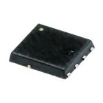


 工商网监
湘ICP备2023018690号
工商网监
湘ICP备2023018690号
