Order
Now
Product
Folder
Support &
Community
Tools &
Software
Technical
Documents
CSD17507Q5A
SLPS243G – JULY 2010 – REVISED JANUARY 2017
CSD17507Q5A 30-V N-Channel NexFET™ Power MOSFET
1 Features
•
•
•
•
•
•
•
1
Product Summary
Ultra-Low Qg and Qgd
Low-Thermal Resistance
Avalanche Rated
Lead-Free Terminal Plating
RoHS Compliant
Halogen Free
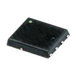
SON 5-mm × 6-mm Plastic Package
TA = 25°C
•
Point-of-Load Synchronous Buck in Networking,
Telecom and Computing Systems
Optimized for Control FET Applications
3 Description
This 30-V, 9-mΩ, SON 5-mm × 6-mm NexFET™
power MOSFET has been designed to minimize
losses in power conversion applications.
30
V
Qg
Gate Charge Total (4.5 V)
2.8
nC
Qgd
Gate Charge Gate-to-Drain
0.7
RDS(on)
Drain-to-Source On Resistance
VGS(th)
Threshold Voltage
Top View
S
1
8
D
S
2
7
D
11.8
VGS = 10 V
9
1.6
mΩ
V
Device Information(1)
DEVICE
MEDIA
QTY
PACKAGE
SHIP
CSD17507Q5A
13-Inch Reel
2500
CSD17507Q5AT
7-Inch Reel
250
SON
5.00-mm × 6.00-mm
Plastic Package
Tape
and
Reel
(1) For all available packages, see the orderable addendum at
the end of the data sheet.
Absolute Maximum Ratings
VALUE
UNIT
VDS
Drain-to-Source Voltage
30
V
VGS
Gate-to-Source Voltage
±20
V
Continuous Drain Current
65
Continuous Drain Current (Silicon Limited),
TC = 25°C
61
ID
(1)
6
3
D
IDM
D
G
nC
VGS = 4.5 V
TA = 25°C (unless otherwise stated)
S
UNIT
Drain-to-Source Voltage
.
2 Applications
•
TYPICAL VALUE
VDS
5
4
PD
D
P0093-01
.
.
Continuous Drain Current
14
Pulsed Drain Current, TC = 25°C(2)
163
Power Dissipation(1)
3.1
Power Dissipation, TC = 25°C
39
TJ,
TSTG
Operating Junction,
Storage Temperature
EAS
Avalanche Energy, Single Pulse
ID = 30 A, L = 0.1 mH, RG = 25 Ω
A
A
W
–55 to 150
°C
45
mJ
(1) Typical RθJA = 40°C/W on a 1-in2, 2-oz Cu pad on a
0.06-in thick FR4 PCB.
(2) Max RθJC = 2°C/W, pulse duration ≤ 100 μs, duty cycle ≤ 1%.
RDS(on) vs VGS
Gate Charge
10
TC = 25qC, ID = 11 A
TC = 125qC, ID = 11 A
25
VGS - Gate-to-Source Voltage (V)
RDS(on) - On-State Resistance (m:)
30
20
15
10
5
0
ID = 11 A
9 VDS = 15 V
8
7
6
5
4
3
2
1
0
0
2
4
6
8
10
12
14
16
VGS - Gate-to-Source Voltage (V)
18
20
D007
0
1
2
3
4
Qg - Gate Charge (nC)
5
6
D004
1
An IMPORTANT NOTICE at the end of this data sheet addresses availability, warranty, changes, use in safety-critical applications,
intellectual property matters and other important disclaimers. PRODUCTION DATA.
�CSD17507Q5A
SLPS243G – JULY 2010 – REVISED JANUARY 2017
www.ti.com
Table of Contents
1
2
3
4
5
Features ..................................................................
Applications ...........................................................
Description .............................................................
Revision History.....................................................
Specifications.........................................................
1
1
1
2
4
5.1 Electrical Characteristics........................................... 4
5.2 Thermal Information .................................................. 4
5.3 Typical MOSFET Characteristics.............................. 5
6
Device and Documentation Support.................... 8
6.1 Receiving Notification of Documentation Updates.... 8
6.2
6.3
6.4
6.5
7
Community Resources..............................................
Trademarks ...............................................................
Electrostatic Discharge Caution ................................
Glossary ....................................................................
8
8
8
8
Mechanical, Packaging, and Orderable
Information ............................................................. 9
7.1
7.2
7.3
7.4
Q5A Package Dimensions ........................................ 9
Recommended PCB Pattern................................... 10
Recommended Stencil Opening ............................. 11
Q5A Tape and Reel Information ............................. 11
4 Revision History
NOTE: Page numbers for previous revisions may differ from page numbers in the current version.
Changes from Revision F (November 2016) to Revision G
•
Page
Corrected package size in the Description section ................................................................................................................ 1
Changes from Revision E (July 2011) to Revision F
Page
•
Changed Description text. ..................................................................................................................................................... 1
•
Added silicon limited continuous drain current to Absolute Maximum Ratings table. ........................................................... 1
•
Changed Note 2 in Absolute Maximum Ratings table. .......................................................................................................... 1
•
Changed THERMAL CHARACTERISTICS table to Thermal Information table. ................................................................... 4
•
Changed RθJC from 1.9°C/W : to 2.1°C/W. ............................................................................................................................ 4
•
Changed RθJA from 51°C/W : to 50°C/W. .............................................................................................................................. 4
•
Added Device and Documentation Support section. ............................................................................................................. 8
•
Changed MECHANICAL DATA section to Mechanical, Packaging, and Orderable Information section. ............................ 9
Changes from Revision D (December 2010) to Revision E
Page
•
Changed VGS in the Abs Max Ratings table From: +20/-12 V To: ±20 V. ............................................................................. 1
•
Changed IGSS Test Conditions from VGS = 20 V +20/-12 V : to VGS = 20 V. ......................................................................... 4
Changes from Revision C (November 2010) to Revision D
•
Changed gfs Transconductance TYP value From: 16 S To: 44 S. ........................................................................................ 4
Changes from Revision B (September 2010) to Revision C
•
2
Page
Added Stencil Recommendation illustration. ....................................................................................................................... 11
Changes from Revision A (August 2010) to Revision B
•
Page
Page
Absolute Maximum Ratings, changed the EAS value from 145 to 45 mJ. ............................................................................. 1
Submit Documentation Feedback
Copyright © 2010–2017, Texas Instruments Incorporated
Product Folder Links: CSD17507Q5A
�CSD17507Q5A
www.ti.com
SLPS243G – JULY 2010 – REVISED JANUARY 2017
Changes from Original (July 2010) to Revision A
•
Page
Changed the Y axis scale for Figure 5. ................................................................................................................................. 5
Submit Documentation Feedback
Copyright © 2010–2017, Texas Instruments Incorporated
Product Folder Links: CSD17507Q5A
3
�CSD17507Q5A
SLPS243G – JULY 2010 – REVISED JANUARY 2017
www.ti.com
5 Specifications
5.1 Electrical Characteristics
TA = 25°C (unless otherwise stated)
PARAMETER
TEST CONDITIONS
MIN
TYP
MAX
UNIT
STATIC CHARACTERISTICS
BVDSS
Drain-to-source voltage
VGS = 0 V, IDS = 250 μA
IDSS
Drain-to-source leakage current
VGS = 0 V, VDS = 24 V
1
μA
IGSS
Gate-to-source leakage current
VDS = 0 V, VGS = 20 V
100
nA
VGS(th)
Gate-to-source threshold voltage
VDS = VGS, IDS = 250 μA
V
RDS(on)
Drain-to-source on resistance
gfs
Transconductance
30
1.1
V
1.6
2.1
VGS = 4.5 V, IDS = 11 A
11.8
16.1
VGS = 10 V, IDS = 11 A
9.0
10.8
VDS = 15 V, IDS = 11 A
44
mΩ
S
DYNAMIC CHARACTERISTICS
Ciss
Input capacitance
Coss
Output capacitance
Crss
Reverse transfer capacitance
RG
Series gate resistance
Qg
Gate charge total (4.5 V)
2.8
Qgd
Gate charge gate-to-drain
Qgs
Gate charge gate-to-source
Qg(th)
Gate charge at Vth
Qoss
Output charge
td(on)
Turnon delay time
tr
Rise time
td(off)
Turnoff delay time
tf
Fall time
VGS = 0 V, VDS = 15 V,
ƒ = 1 MHz
VDS = 15 V, IDS = 11 A
VDS = 13 V, VGS = 0 V
VDS = 15 V, VGS = 4.5 V,
IDS = 11 A, RG = 2 Ω
410
530
pF
270
350
pF
23
30
pF
0.7
1.4
Ω
3.6
nC
0.7
nC
1.3
nC
0.7
nC
7.2
nC
4.7
ns
5.2
ns
5.7
ns
2.3
ns
DIODE CHARACTERISTICS
VSD
Diode forward voltage
Qrr
Reverse recovery charge
trr
Reverse recovery time
ISD = 11 A, VGS = 0 V
0.85
VDS= 13 V, IF = 11 A, di/dt = 300 A/μs
1
V
11
nC
16
ns
5.2 Thermal Information
TA = 25°C (unless otherwise stated)
MAX
UNIT
RθJC
Thermal resistance junction-to-case (1)
PARAMETER
2.1
°C/W
RθJA
Thermal resistance junction-to-ambient (1) (2)
50
°C/W
(1)
(2)
4
MIN
TYP
RθJC is determined with the device mounted on a 1-in2 (6.45-cm2), 2-oz (0.071-mm) thick Cu pad on a 1.5-in × 1.5-in (3.81-cm × 3.81cm), 0.06-in (1.52-mm) thick FR4 PCB. RθJC is specified by design, whereas RθJA is determined by the user’s board design.
Device mounted on FR4 material with 1-in2 (6.45-cm2), 2-oz (0.071-mm) thick Cu.
Submit Documentation Feedback
Copyright © 2010–2017, Texas Instruments Incorporated
Product Folder Links: CSD17507Q5A
�CSD17507Q5A
www.ti.com
GATE
SLPS243G – JULY 2010 – REVISED JANUARY 2017
GATE
Source
N-Chan 5x6 QFN TTA MIN Rev3
N-Chan 5x6 QFN TTA MAX Rev3
Max RθJA = 50°C/W
when mounted on 1 in2
(6.45 cm2) of 2-oz
(0.071-mm) thick Cu.
Source
Max RθJA = 125°C/W
when mounted on a
minimum pad area of
2-oz (0.071-mm) thick
Cu.
DRAIN
DRAIN
M0137-02
M0137-01
5.3 Typical MOSFET Characteristics
TA = 25°C (unless otherwise stated)
Figure 1. Transient Thermal Impedance
Submit Documentation Feedback
Copyright © 2010–2017, Texas Instruments Incorporated
Product Folder Links: CSD17507Q5A
5
�CSD17507Q5A
SLPS243G – JULY 2010 – REVISED JANUARY 2017
www.ti.com
Typical MOSFET Characteristics (continued)
100
100
90
90
IDS - Drain-to-Source Current (A)
IDS - Drain-to-Source Current (A)
TA = 25°C (unless otherwise stated)
80
70
60
50
40
30
20
VGS = 4.5 V
VGS = 6 V
VGS = 10 V
10
TC = 125° C
TC = 25° C
TC = -55° C
80
70
60
50
40
30
20
10
0
0
0
0.5
1
1.5
2
2.5
3
3.5
4
VDS - Drain-to-Source Voltage (V)
4.5
5
1
1.5
2
D002
2.5
3
3.5
4
4.5
5
VGS - Gate-to-Source Voltage (V)
5.5
6
D003
VDS = 5 V
Figure 2. Saturation Characteristics
Figure 3. Transfer Characteristics
10000
ID = 11 A
9 VDS = 15 V
Ciss = Cgd + Cgs
Coss = Cds + Cgd
Crss = Cgd
8
C - Capacitance (pF)
VGS - Gate-to-Source Voltage (V)
10
7
6
5
4
3
1000
100
2
1
10
0
0
1
2
3
4
Qg - Gate Charge (nC)
ID = 11 A
5
0
6
5
D004
Figure 4. Gate Charge
D005
Figure 5. Capacitance
RDS(on) - On-State Resistance (m:)
VGS(th) - Threshold Voltage (V)
30
30
2
1.8
1.6
1.4
1.2
1
TC = 25qC, ID = 11 A
TC = 125qC, ID = 11 A
25
20
15
10
5
0
-50
-25
0
25
50
75 100
TC - Case Temperature (qC)
125
150
175
0
2
D006
ID = 250 µA
4
6
8
10
12
14
16
VGS - Gate-to-Source Voltage (V)
18
20
D007
ID = 11 A
Figure 6. Threshold Voltage vs Temperature
6
25
VDS = 15 V
2.2
0.8
-75
10
15
20
VDS - Drain-to-Source Voltage (V)
Figure 7. On-State Resistance vs Gate-to-Source Voltage
Submit Documentation Feedback
Copyright © 2010–2017, Texas Instruments Incorporated
Product Folder Links: CSD17507Q5A
�CSD17507Q5A
www.ti.com
SLPS243G – JULY 2010 – REVISED JANUARY 2017
Typical MOSFET Characteristics (continued)
TA = 25°C (unless otherwise stated)
100
1.6
ISD - Source-to-Drain Current (A)
Normalized On-State Resistance
1.8
1.4
1.2
1
0.8
0.6
0.4
-75
-50
-25
0
25
50
75 100
TC - Case Temperature (° C)
125
150
175
TC = 25° C
TC = 125° C
10
1
0.1
0.01
0.001
0.0001
0.2
0.4
D008
0.6
0.8
1
VSD - Source-to-Drain Voltage (V)
1.2
D009
ID = 11 A, VGS = 10 V
Figure 8. Normalized On-State Resistance vs Temperature
Figure 9. Typical Diode Forward Voltage
100
IAV - Peak Avalanche Current (A)
IDS - Drain-to-Source Current (A)
1000
100
10
1
DC
10 ms
1 ms
0.1
0.1
100 µs
10 µs
1
10
VDS - Drain-to-Source Voltage (V)
100
TC = 25q C
TC = 125q C
10
1
0.01
0.1
1
TAV - Time in Avalanche (ms)
D010
10
D011
Single pulse, max RθJC = 2.1°C/W
Figure 10. Maximum Safe Operating Area
Figure 11. Single Pulse Unclamped Inductive Switching
IDS - Drain-to-Source Current (A)
80
70
60
50
40
30
20
10
0
-50
-25
0
25
50
75
100 125
TC - Case Temperature (° C)
150
175
D012
Figure 12. Maximum Drain Current vs Temperature
Submit Documentation Feedback
Copyright © 2010–2017, Texas Instruments Incorporated
Product Folder Links: CSD17507Q5A
7
�CSD17507Q5A
SLPS243G – JULY 2010 – REVISED JANUARY 2017
www.ti.com
6 Device and Documentation Support
6.1 Receiving Notification of Documentation Updates
To receive notification of documentation updates, navigate to the device product folder on ti.com. In the upper
right corner, click on Alert me to register and receive a weekly digest of any product information that has
changed. For change details, review the revision history included in any revised document.
6.2 Community Resources
The following links connect to TI community resources. Linked contents are provided "AS IS" by the respective
contributors. They do not constitute TI specifications and do not necessarily reflect TI's views; see TI's Terms of
Use.
TI E2E™ Online Community TI's Engineer-to-Engineer (E2E) Community. Created to foster collaboration
among engineers. At e2e.ti.com, you can ask questions, share knowledge, explore ideas and help
solve problems with fellow engineers.
Design Support TI's Design Support Quickly find helpful E2E forums along with design support tools and
contact information for technical support.
6.3 Trademarks
NexFET, E2E are trademarks of Texas Instruments.
All other trademarks are the property of their respective owners.
6.4 Electrostatic Discharge Caution
These devices have limited built-in ESD protection. The leads should be shorted together or the device placed in conductive foam
during storage or handling to prevent electrostatic damage to the MOS gates.
6.5 Glossary
SLYZ022 — TI Glossary.
This glossary lists and explains terms, acronyms, and definitions.
8
Submit Documentation Feedback
Copyright © 2010–2017, Texas Instruments Incorporated
Product Folder Links: CSD17507Q5A
�CSD17507Q5A
www.ti.com
SLPS243G – JULY 2010 – REVISED JANUARY 2017
7 Mechanical, Packaging, and Orderable Information
The following pages include mechanical, packaging, and orderable information. This information is the most
current data available for the designated devices. This data is subject to change without notice and revision of
this document. For browser-based versions of this data sheet, refer to the left-hand navigation.
2
3
4
5
4
5
6
3
6
7
2
7
1
8
1
8
7.1 Q5A Package Dimensions
DIM
MILLIMETERS
MIN
NOM
MAX
A
0.90
1.00
1.10
b
0.33
0.41
0.51
c
0.20
0.25
0.34
D1
4.80
4.90
5.00
D2
3.61
3.81
4.02
E
5.90
6.00
6.10
E1
5.70
5.75
5.80
E2
3.38
3.58
3.78
E3
3.03
3.13
3.23
e
1.17
1.27
1.37
e1
0.27
0.37
0.47
e2
0.15
0.25
0.35
H
0.41
0.56
0.71
K
1.10
—
—
L
0.51
0.61
0.71
L1
0.06
0.13
0.20
0°
—
12°
θ
Submit Documentation Feedback
Copyright © 2010–2017, Texas Instruments Incorporated
Product Folder Links: CSD17507Q5A
9
�CSD17507Q5A
SLPS243G – JULY 2010 – REVISED JANUARY 2017
www.ti.com
7.2 Recommended PCB Pattern
F1
F7
8
F3
1
F2
F11
F5
F9
5
4
F6
F8
F4
F10
M0139-01
DIM
MILLIMETERS
INCHES
MIN
MAX
MIN
MAX
F1
6.205
6.305
0.244
0.248
F2
4.46
4.56
0.176
0.18
F3
4.46
4.56
0.176
0.18
F4
0.65
0.7
0.026
0.028
F5
0.62
0.67
0.024
0.026
F6
0.63
0.68
0.025
0.027
F7
0.7
0.8
0.028
0.031
F8
0.65
0.7
0.026
0.028
F9
0.62
0.67
0.024
0.026
F10
4.9
5
0.193
0.197
F11
4.46
4.56
0.176
0.18
For recommended circuit layout for PCB designs, see Reducing Ringing Through PCB Layout Techniques
(SLPA005).
10
Submit Documentation Feedback
Copyright © 2010–2017, Texas Instruments Incorporated
Product Folder Links: CSD17507Q5A
�CSD17507Q5A
www.ti.com
SLPS243G – JULY 2010 – REVISED JANUARY 2017
7.3 Recommended Stencil Opening
(0.020) 8x
0.500
(0.020)
0.500
5
4
0.500
(0.020) 8x
1.585
(0.062)
1.235
(0.049)
(0.024)
0.620
(0.170) 4.310
0.385
(0.015)
1.270 (0.050)
1
8
1.570 (0.062)
4x
0.615
(0.024)
1.105
(0.044)
3.020
(0.119)
K0
4.00 ±0.10 (See Note 1)
0.30 ±0.05
2.00 ±0.05
+0.10
–0.00
12.00 ±0.30
Ø 1.50
1.75 ±0.10
7.4 Q5A Tape and Reel Information
5.50 ±0.05
B0
R 0.30 MAX
A0
8.00 ±0.10
Ø 1.50 MIN
A0 = 6.50 ±0.10
B0 = 5.30 ±0.10
K0 = 1.40 ±0.10
R 0.30 TYP
M0138-01
Notes:
1. 10-sprocket hole-pitch cumulative tolerance ±0.2.
2. Camber not to exceed 1 mm in 100 mm, noncumulative over 250 mm.
3. Material: black static-dissipative polystyrene.
4. All dimensions are in mm (unless otherwise specified).
5. A0 and B0 measured on a plane 0.3 mm above the bottom of the pocket.
Submit Documentation Feedback
Copyright © 2010–2017, Texas Instruments Incorporated
Product Folder Links: CSD17507Q5A
11
�PACKAGE OPTION ADDENDUM
www.ti.com
10-Dec-2020
PACKAGING INFORMATION
Orderable Device
Status
(1)
Package Type Package Pins Package
Drawing
Qty
Eco Plan
(2)
Lead finish/
Ball material
MSL Peak Temp
Op Temp (°C)
Device Marking
(3)
(4/5)
(6)
CSD17507Q5A
ACTIVE
VSONP
DQJ
8
2500
RoHS-Exempt
& Green
SN
Level-1-260C-UNLIM
-55 to 150
CSD17507
CSD17507Q5AT
ACTIVE
VSONP
DQJ
8
250
RoHS-Exempt
& Green
SN
Level-1-260C-UNLIM
-55 to 150
CSD17507
(1)
The marketing status values are defined as follows:
ACTIVE: Product device recommended for new designs.
LIFEBUY: TI has announced that the device will be discontinued, and a lifetime-buy period is in effect.
NRND: Not recommended for new designs. Device is in production to support existing customers, but TI does not recommend using this part in a new design.
PREVIEW: Device has been announced but is not in production. Samples may or may not be available.
OBSOLETE: TI has discontinued the production of the device.
(2)
RoHS: TI defines "RoHS" to mean semiconductor products that are compliant with the current EU RoHS requirements for all 10 RoHS substances, including the requirement that RoHS substance
do not exceed 0.1% by weight in homogeneous materials. Where designed to be soldered at high temperatures, "RoHS" products are suitable for use in specified lead-free processes. TI may
reference these types of products as "Pb-Free".
RoHS Exempt: TI defines "RoHS Exempt" to mean products that contain lead but are compliant with EU RoHS pursuant to a specific EU RoHS exemption.
Green: TI defines "Green" to mean the content of Chlorine (Cl) and Bromine (Br) based flame retardants meet JS709B low halogen requirements of