CSD23201W10
www.ti.com
SLPS209A – AUGUST 2009 – REVISED MAY 2010
P-Channel NexFET™ Power MOSFET
Check for Samples: CSD23201W10
FEATURES
1
•
•
•
•
•
•
•
PRODUCT SUMMARY
Ultra Low Qg and Qgd
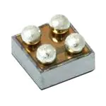
Small Footprint 1mm × 1mm
Low Profile 0.62mm Height
Pb Free
Gate ESD Protection – 3kV
RoHS Compliant
Halogen Free
VDS
Drain to Source Voltage
–12
V
Qg
Gate Charge Total (4.5V)
1.8
nC
Qgd
Gate Charge Gate to Drain
RDS(on)
VGS(th)
Drain to Source On Resistance
nC
110
mΩ
VGS = –2.5V
77
mΩ
VGS = –4.5V
66
mΩ
Threshold Voltage
–0.6
V
ORDERING INFORMATION
APPLICATIONS
•
•
•
0.26
VGS = –1.5V
Battery Management
Load Switch
Battery Protection
Device
Package
CSD23201W10
1 × 1 Wafer Level
Package
Media
7-inch reel
Qty
Ship
3000
Tape and
Reel
ABSOLUTE MAXIMUM RATINGS
DESCRIPTION
TA = 25°C unless otherwise stated
The device has been designed to deliver the lowest
on resistance and gate charge in the smallest outline
possible with excellent thermal characteristics in an
ultra low profile.
D
D
UNIT
–12
V
–6
V
–2.2
A
Drain to Source Voltage
VGS
Gate to Source Voltage
ID
Continuous Drain Current, TC = 25°C(1)
IDM
Pulsed Drain Current, TA = 25°C(2)
–8.8
A
Continuous Gate Clamp Current
–0.5
A
IG
Top View
VALUE
VDS
Pulsed Gate Clamp Current
–7
A
PD
Power Dissipation(1)
1
W
TJ,
TSTG
Operating Junction and Storage
Temperature Range
–55 to 150
°C
(1) RqJA = 100°C/W on 1in2 Cu (2 oz.) on 0.060" thick FR4 PCB.
(2) Pulse width ≤300ms, duty cycle ≤2%
G
S
P0097-01
RDS(ON) vs VGS
Gate Charge
4.5
ID = −0.5A
180
4.0
160
−VG − Gate Voltage − V
RDS(on) − On-State Resistance − mΩ
200
140
TC = 125°C
120
100
80
60
40
TC = 25°C
ID = −0.5A
VDS = −6V
3.5
3.0
2.5
2.0
1.5
1.0
0.5
20
0
0
1
2
3
4
−VGS − Gate to Source Voltage − V
5
6
G006
0.0
0.00
0.25
0.50
0.75
1.00
1.25
1.50
1.75
2.00
Qg − Gate Charge − nC
G003
1
Please be aware that an important notice concerning availability, standard warranty, and use in critical applications of Texas
Instruments semiconductor products and disclaimers thereto appears at the end of this data sheet.
PRODUCTION DATA information is current as of publication date.
Products conform to specifications per the terms of the Texas
Instruments standard warranty. Production processing does not
necessarily include testing of all parameters.
Copyright © 2009–2010, Texas Instruments Incorporated
�CSD23201W10
SLPS209A – AUGUST 2009 – REVISED MAY 2010
www.ti.com
These devices have limited built-in ESD protection. The leads should be shorted together or the device placed in conductive foam
during storage or handling to prevent electrostatic damage to the MOS gates.
ELECTRICAL CHARACTERISTICS
(TA = 25°C unless otherwise stated)
PARAMETER
TEST CONDITIONS
MIN
TYP
MAX
UNIT
Static Characteristics
BVDSS
Drain to Source Voltage
VGS = 0V, ID = –250mA
–12
BVGSS
Gate to Source Voltage;
VDS = 0V, IG = –250mA
–6.1
IDSS
Drain to Source Leakage Current
VGS = 0V, VDS = –9.6V
IGSS
Gate to Source Leakage Current
VDS = 0V, VGS = –6V
VGS(th)
Gate to Source Threshold Voltage
VDS = VGS, ID = –250mA
RDS(on)
gfs
Drain to Source On Resistance
Transconductance
–0.4
V
–7.2
V
–1
mA
–100
nA
–0.6
–1.0
V
VGS = –1.5V, ID = –0.5A
110
138
mΩ
VGS = –2.5V, ID = –0.5A
77
96
mΩ
VGS = –4.5V, ID = –0.5A
66
82
mΩ
VDS = –6.0V, ID = –0.5A
9
S
Dynamic Characteristics
CISS
Input Capacitance
COSS
Output Capacitance
250
325
pF
125
155
CRSS
Reverse Transfer Capacitance
pF
32
42
pF
Qg
Qgd
Gate Charge Total (–4.5V)
1.8
2.4
nC
Gate Charge Gate to Drain
0.26
Qgs
Gate Charge Gate to Source
nC
0.28
nC
Qg(th)
Gate Charge at Vth
QOSS
Output Charge
0.11
nC
1.7
td(on)
Turn On Delay Time
nC
24
ns
tr
Rise Time
td(off)
Turn Off Delay Time
19
ns
68
tf
Fall Time
ns
29
ns
VGS = 0V, VDS = –6.0V, f = 1MHz
VDS = –6.0V, ID = –0.5A
VDS = –6.0V, VGS = 0V
VDS = –6.0V, VGS = –2.5V, ID = –0.5A
RG = 20Ω
Diode Characteristics
VSD
Diode Forward Voltage
IS = –0.5A, VGS = 0V
Qrr
Reverse Recovery Charge
Vdd= –4.0V, IF = –0.5A, di/dt = 100A/ms
–0.77
2
–1.0
nC
V
trr
Reverse Recovery Time
Vdd= –4.0V, IF = –0.5A, di/dt = 100A/ms
9.5
ns
THERMAL CHARACTERISTICS
(TA = 25°C unless otherwise stated)
PARAMETER
R qJC
R qJA
2
Thermal Resistance Junction to Ambient (Minimum Cu area)
2
Thermal Resistance Junction to Ambient (1 in Cu area)
Submit Documentation Feedback
MIN
TYP
MAX
UNIT
245
°C/W
125
°C/W
Copyright © 2009–2010, Texas Instruments Incorporated
Product Folder Link(s): CSD23201W10
�CSD23201W10
www.ti.com
SLPS209A – AUGUST 2009 – REVISED MAY 2010
P-Chan 1.0x1.0 CSP TTA MAX Rev1
P-Chan 1.0x1.0 CSP TTA MIN Rev1
Max RqJA = 245°C/W
when mounted on
minimum pad area of 2
oz. Cu.
Max RqJA = 125°C/W
when mounted on
1inch2 of 2 oz. Cu.
M0149-01
M0150-01
TYPICAL MOSFET CHARACTERISTICS
(TA = 25°C unless otherwise stated)
ZqJA – NormalizedThermal Impedance
10
1
0.5
0.3
0.1
0.01
0.1
0.05
Duty Cycle = t1/t2
0.02
0.01
P
t1
t2
0.001
0.0001
0.00001
RqJA = 195°C/W (min Cu)
TJ = P x ZqJA x RqJA
Single Pulse
0.0001
0.001
0.01
0.1
1
10
100
tp – Pulse Duration–s
1k
G012
Figure 1. Transient Thermal Impedance
Submit Documentation Feedback
Copyright © 2009–2010, Texas Instruments Incorporated
Product Folder Link(s): CSD23201W10
3
�CSD23201W10
SLPS209A – AUGUST 2009 – REVISED MAY 2010
www.ti.com
TYPICAL MOSFET CHARACTERISTICS (continued)
(TA = 25°C unless otherwise stated)
5
5
VGS = −1.5V
VGS = −4.5V
−ID − Drain Current − A
−ID − Drain Current − A
VDS = −5V
4
3
VGS = −3V
2
VGS = −2.5V
VGS = −1.2V
1
4
TC = 125°C
3
2
TC = 25°C
1
TC = −55°C
0
0.0
0.3
0.6
0.9
1.2
0
0.50
1.5
−VDS − Drain to Source Voltage − V
0.75
G001
Figure 2. Saturation Characteristics
1.50
1.75
2.00
G002
300
ID = −0.5A
VDS = −6V
f = 1MHz, VGS = 0V
250
3.5
C − Capacitance − pF
−VG − Gate Voltage − V
1.25
Figure 3. Transfer Characteristics
4.5
4.0
1.00
−VGS − Gate to Source Voltage − V
3.0
2.5
2.0
1.5
1.0
COSS = CDS + CGD
200
CISS = CGD + CGS
150
100
CRSS = CGD
50
0.5
0.0
0.00
0
0.25
0.50
0.75
1.00
1.25
1.50
1.75
0
2.00
Qg − Gate Charge − nC
2
10
12
G004
200
RDS(on) − On-State Resistance − mΩ
−VGS(th) − Threshold Voltage − V
8
Figure 5. Capacitance
1.0
ID = −250µA
0.9
0.8
0.7
0.6
0.5
0.4
0.3
0.2
0.1
ID = −0.5A
180
160
140
TC = 125°C
120
100
80
60
40
TC = 25°C
20
0
−25
25
75
125
175
TC − Case Temperature − °C
0
1
2
3
4
5
−VGS − Gate to Source Voltage − V
G005
Figure 6. Threshold Voltage vs. Temperature
4
6
−VDS − Drain to Source Voltage − V
G003
Figure 4. Gate Charge
0.0
−75
4
6
G006
Figure 7. On Resistance vs. Gate Voltage
Submit Documentation Feedback
Copyright © 2009–2010, Texas Instruments Incorporated
Product Folder Link(s): CSD23201W10
�CSD23201W10
www.ti.com
SLPS209A – AUGUST 2009 – REVISED MAY 2010
TYPICAL MOSFET CHARACTERISTICS (continued)
(TA = 25°C unless otherwise stated)
10
1.4
ID = −0.5A
VGS = −4.5V
−ISD − Source to Drain Current − A
Normalized On-State Resistance
1.6
1.2
1.0
0.8
0.6
0.4
0.2
0.0
−75
1
TC = 125°C
0.1
TC = 25°C
0.01
0.001
0.0001
−25
25
75
125
TC − Case Temperature − °C
175
0.0
0.2
0.4
0.6
0.8
1.0
1.2
−VSD − Source to Drain Voltage − V
G007
Figure 8. On Resistance vs. Temperature
G008
Figure 9. Typical Diode Forward Voltage
3.0
100
−ID − Drain Current − A
−ID − Drain Current − A
2.5
10
100ms
1
100ms
0.1
Area Limited
by RDS(on)
10ms
1s
DC
Single Pulse
RθJA = 195°C/W (min Cu)
0.01
0.1
1
10
Figure 10. Maximum Safe Operating Area
1.5
1.0
0.5
100
−VDS − Drain To Source Voltage − V
2.0
0.0
−50
−25
0
25
50
75
100
125
150
175
TC − Case Temperature − °C
G009
G011
Figure 11. Maximum Drain Current vs. Temperature
Submit Documentation Feedback
Copyright © 2009–2010, Texas Instruments Incorporated
Product Folder Link(s): CSD23201W10
5
�CSD23201W10
SLPS209A – AUGUST 2009 – REVISED MAY 2010
www.ti.com
MECHANICAL DATA
CSD23201W10 Package Dimensions
Pin 1
Mark
1
Solder Ball
Ø 0.31 ±0.075
2
2
1
A
1.00
0.50
+0.00
–0.10
A
B
B
1.00
+0.00
–0.10
0.50
Side View
Bottom View
0.04
0.62 Max
0.38
Top View
0.62 Max
Seating Plate
Front View
M0151-01
NOTE: All dimensions are in mm (unless otherwise specified)
Pin Configuration Table
6
POSITION
DESIGNATION
B1
Source
A1
Gate
A2, B2
Drain
Submit Documentation Feedback
Copyright © 2009–2010, Texas Instruments Incorporated
Product Folder Link(s): CSD23201W10
�CSD23201W10
www.ti.com
SLPS209A – AUGUST 2009 – REVISED MAY 2010
Land Pattern Recommendation
Ø 0.25
1
2
0.50
A
B
0.50
M0152-01
NOTE: All dimensions are in mm (unless otherwise specified)
Tape and Reel Information
4.00 ±0.10
2.00 ±0.05
4.00 ±0.10
Ø 0.50 ±0.05
0.78 ±0.05
1.18 ±0.05
5° Max
3.50 ±0.05
8.00
+0.30
–0.10
1.75 ±0.10
Ø 1.50 ±0.10
0.254 ±0.02
1.18 ±0.05
5° Max
M0153-01
NOTE: All dimensions are in mm (unless otherwise specified)
REVISION HISTORY
Changes from Original (August 2009) to Revision A
•
Page
Deleted the Package Marking Information section ............................................................................................................... 7
Submit Documentation Feedback
Copyright © 2009–2010, Texas Instruments Incorporated
Product Folder Link(s): CSD23201W10
7
�IMPORTANT NOTICE
Texas Instruments Incorporated and its subsidiaries (TI) reserve the right to make corrections, modifications, enhancements, improvements,
and other changes to its products and services at any time and to discontinue any product or service without notice. Customers should
obtain the latest relevant information before placing orders and should verify that such information is current and complete. All products are
sold subject to TI’s terms and conditions of sale supplied at the time of order acknowledgment.
TI warrants performance of its hardware products to the specifications applicable at the time of sale in accordance with TI’s standard
warranty. Testing and other quality control techniques are used to the extent TI deems necessary to support this warranty. Except where
mandated by government requirements, testing of all parameters of each product is not necessarily performed.
TI assumes no liability for applications assistance or customer product design. Customers are responsible for their products and
applications using TI components. To minimize the risks associated with customer products and applications, customers should provide
adequate design and operating safeguards.
TI does not warrant or represent that any license, either express or implied, is granted under any TI patent right, copyright, mask work right,
or other TI intellectual property right relating to any combination, machine, or process in which TI products or services are used. Information
published by TI regarding third-party products or services does not constitute a license from TI to use such products or services or a
warranty or endorsement thereof. Use of such information may require a license from a third party under the patents or other intellectual
property of the third party, or a license from TI under the patents or other intellectual property of TI.
Reproduction of TI information in TI data books or data sheets is permissible only if reproduction is without alteration and is accompanied
by all associated warranties, conditions, limitations, and notices. Reproduction of this information with alteration is an unfair and deceptive
business practice. TI is not responsible or liable for such altered documentation. Information of third parties may be subject to additional
restrictions.
Resale of TI products or services with statements different from or beyond the parameters stated by TI for that product or service voids all
express and any implied warranties for the associated TI product or service and is an unfair and deceptive business practice. TI is not
responsible or liable for any such statements.
TI products are not authorized for use in safety-critical applications (such as life support) where a failure of the TI product would reasonably
be expected to cause severe personal injury or death, unless officers of the parties have executed an agreement specifically governing
such use. Buyers represent that they have all necessary expertise in the safety and regulatory ramifications of their applications, and
acknowledge and agree that they are solely responsible for all legal, regulatory and safety-related requirements concerning their products
and any use of TI products in such safety-critical applications, notwithstanding any applications-related information or support that may be
provided by TI. Further, Buyers must fully indemnify TI and its representatives against any damages arising out of the use of TI products in
such safety-critical applications.
TI products are neither designed nor intended for use in military/aerospace applications or environments unless the TI products are
specifically designated by TI as military-grade or "enhanced plastic." Only products designated by TI as military-grade meet military
specifications. Buyers acknowledge and agree that any such use of TI products which TI has not designated as military-grade is solely at
the Buyer's risk, and that they are solely responsible for compliance with all legal and regulatory requirements in connection with such use.
TI products are neither designed nor intended for use in automotive applications or environments unless the specific TI products are
designated by TI as compliant with ISO/TS 16949 requirements. Buyers acknowledge and agree that, if they use any non-designated
products in automotive applications, TI will not be responsible for any failure to meet such requirements.
Following are URLs where you can obtain information on other Texas Instruments products and application solutions:
Products
Applications
Audio
www.ti.com/audio
Communications and Telecom www.ti.com/communications
Amplifiers
amplifier.ti.com
Computers and Peripherals
www.ti.com/computers
Data Converters
dataconverter.ti.com
Consumer Electronics
www.ti.com/consumer-apps
DLP® Products
www.dlp.com
Energy and Lighting
www.ti.com/energy
DSP
dsp.ti.com
Industrial
www.ti.com/industrial
Clocks and Timers
www.ti.com/clocks
Medical
www.ti.com/medical
Interface
interface.ti.com
Security
www.ti.com/security
Logic
logic.ti.com
Space, Avionics and Defense
www.ti.com/space-avionics-defense
Power Mgmt
power.ti.com
Transportation and
Automotive
www.ti.com/automotive
Microcontrollers
microcontroller.ti.com
Video and Imaging
www.ti.com/video
RFID
www.ti-rfid.com
Wireless
www.ti.com/wireless-apps
RF/IF and ZigBee® Solutions
www.ti.com/lprf
TI E2E Community Home Page
e2e.ti.com
Mailing Address: Texas Instruments, Post Office Box 655303, Dallas, Texas 75265
Copyright © 2011, Texas Instruments Incorporated
�