Order
Now
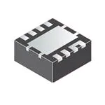
Product
Folder
Support &
Community
Tools &
Software
Technical
Documents
CSD87334Q3D
SLPS546A – JULY 2015 – REVISED MARCH 2017
CSD87334Q3D Synchronous Buck NexFET™ Power Block
1 Features
3 Description
•
•
•
•
•
•
•
•
•
•
•
•
•
•
The CSD87334Q3D NexFET™ power block is an
optimized design for synchronous buck and boost
applications offering high-current, high-efficiency, and
high-frequency capability in a small 3.3 mm × 3.3 mm
outline. Optimized for 5-V gate drive applications, this
product offers a flexible solution in high-duty cycle
applications when paired with an external controller or
driver.
1
Half-Bridge Power Block
Optimized for High-Duty Cycle
Up to 24 Vin
96.1% System Efficiency at 12 A
1.6-W PLoss at 12 A
Up to 20-A Operation
High-Frequency Operation (up to 1.5 MHz)
High-Density SON 3.3 mm × 3.3 mm Footprint
Optimized for 5-V Gate Drive
Low-Switching Losses
Ultra-Low-Inductance Package
RoHS Compliant
Halogen-Free
Lead-Free Terminal Plating
.
TOP VIEW
2 Applications
8
VSW
7
VSW
3
6
VSW
4
5
BG
VIN
1
VIN
2
TG
TGR
PGND
(Pin 9)
P0116-01
•
•
•
Synchronous Buck Converters
– High-Frequency Applications
– High-Duty Cycle Applications
Synchronous Boost Converters
POL DC-DC Converters
Device Information(1)
DEVICE
QTY
MEDIA
PACKAGE
SHIP
CSD87334Q3D
2500
13-Inch Reel
CSD87334Q3DT
250
7-Inch Reel
SON
3.30-mm × 3.30-mm
Plastic Package
Tape
and
Reel
(1) For all available packages, see the orderable addendum at
the end of the data sheet.
.
.
Typical Circuit
Typical Power Block Efficiency and Power Loss
VIN
VDD
VDD
100
5
90
4
BOOT
TGR
ENABLE
PWM
ENABLE
PWM
VSW
LL
DRVL
VOUT
BG
PGND
Driver IC
Efficiency (%)
GND
TG
VGS = 5 V
80 V = 12 V
IN
VOUT = 3.3 V
LOUT = 1.0 PH
70 fSW = 500 kHz
TA = 25qC
3
2
Power Loss (W)
VIN
DRVH
CSD87334Q3D
60
1
50
0
5
10
Output Current (A)
15
0
20
D000
1
An IMPORTANT NOTICE at the end of this data sheet addresses availability, warranty, changes, use in safety-critical applications,
intellectual property matters and other important disclaimers. PRODUCTION DATA.
�CSD87334Q3D
SLPS546A – JULY 2015 – REVISED MARCH 2017
www.ti.com
Table of Contents
1
2
3
4
5
6
Features ..................................................................
Applications ...........................................................
Description .............................................................
Revision History.....................................................
Specifications.........................................................
1
1
1
2
3
5.1
5.2
5.3
5.4
5.5
5.6
5.7
3
3
3
3
4
5
7
Absolute Maximum Ratings ......................................
Recommended Operating Conditions.......................
Power Block Performance ........................................
Thermal Information ..................................................
Electrical Characteristics...........................................
Typical Power Block Device Characteristics.............
Typical Power Block MOSFET Characteristics.........
Application and Implementation .......................... 9
6.1 Application Information.............................................. 9
6.2 Typical Application .................................................... 9
6.3 System Example ....................................................... 9
7
Layout ................................................................... 12
7.1 Layout Guidelines ................................................... 12
7.2 Layout Example ...................................................... 13
7.3 Thermal Considerations .......................................... 13
8
Device and Documentation Support.................. 14
8.1
8.2
8.3
8.4
8.5
9
Receiving Notification of Documentation Updates.. 14
Community Resources............................................ 14
Trademarks ............................................................. 14
Electrostatic Discharge Caution .............................. 14
Glossary .................................................................. 14
Mechanical, Packaging, and Orderable
Information ........................................................... 15
9.1
9.2
9.3
9.4
Q3D Package Dimensions......................................
Land Pattern Recommendation ..............................
Stencil Recommendation ........................................
Q3D Tape and Reel Information .............................
15
16
17
17
4 Revision History
Changes from Original (August 2015) to Revision A
Page
•
Changed TG to TGR minimum voltage, from –8 V : to –0.3 V in Absolute Maximum Ratings table ....................................... 3
•
Changed BG to PGND minimum voltage, from –8 V : to –0.3 V in Absolute Maximum Ratings table ..................................... 3
•
Changed IGSS test condition for VGS, from +10 / –8 V : to 10 V in Electrical Characteristics table ........................................ 4
•
Added Receiving Notification of Documentation Updates section and Community Resources section to Device and
Documentation Support section ........................................................................................................................................... 14
2
Submit Documentation Feedback
Copyright © 2015–2017, Texas Instruments Incorporated
Product Folder Links: CSD87334Q3D
�CSD87334Q3D
www.ti.com
SLPS546A – JULY 2015 – REVISED MARCH 2017
5 Specifications
5.1 Absolute Maximum Ratings
TA = 25°C (unless otherwise noted) (see
(1)
)
MIN
Voltage
MAX
VIN to PGND
30
VSW to PGND
30
VSW to PGND (10 ns)
UNIT
32
TG to TGR
–0.3
10
BG to PGND
–0.3
10
V
IDM
Pulsed current rating
60
A
PD
Power dissipation
6
W
EAS
Avalanche energy
TJ
Operating junction temperature
–55
150
°C
Tstg
Storage temperature
–55
150
°C
(1)
Sync FET, ID = 31 A, L = 0.1 mH
48
Control FET, ID = 31 A, L = 0.1 mH
48
mJ
Stresses beyond those listed under Absolute Maximum Ratings may cause permanent damage to the device. These are stress ratings
only, and functional operation of the device at these or any other conditions beyond those indicated in the Recommended Operating
Conditions is not implied. Exposure to absolute-maximum-rated conditions for extended periods may affect device reliability.
5.2 Recommended Operating Conditions
TA = 25°C (unless otherwise noted)
VGS
Gate drive voltage
VIN
Input supply voltage
ƒSW
Switching frequency
MIN
MAX
3.3
8
V
24
V
CBST = 0.1 µF (min)
1500
Operating current
TJ
Operating temperature
UNIT
kHz
20
A
125
°C
5.3 Power Block Performance
TA = 25°C (unless otherwise noted) (see
(1)
)
PARAMETER
TEST CONDITIONS
PLOSS
Power loss (1)
VIN = 12 V, VGS = 5 V, VOUT = 3.3 V,
IOUT = 12 A, ƒSW = 500 kHz,
LOUT = 1 µH, TJ = 25°C
IQVIN
VIN quiescent current
TG to TGR = 0 V BG to PGND = 0 V
(1)
MIN
TYP
MAX
UNIT
1.6
W
10
µA
Measurement made with six 10-µF (TDK C3216X5R1C106KT or equivalent) ceramic capacitors placed across VIN to PGND pins and
using a high current 5-V driver IC.
5.4 Thermal Information
TA = 25°C (unless otherwise stated)
THERMAL METRIC
RθJA
RθJC
(1)
(2)
Junction-to-ambient thermal resistance (min Cu) (1)
Junction-to-ambient thermal resistance (max Cu) (1) (2)
MIN
TYP
MAX
130
75
Junction-to-case thermal resistance (top of package) (1)
21
Junction-to-case thermal resistance (PGND pin) (1)
2.1
UNIT
°C/W
°C/W
RθJC is determined with the device mounted on a 1-in2 (6.45-cm2), 2-oz (0.071-mm) thick Cu pad on a 1.5-in × 1.5-in
(3.81-cm × 3.81-cm), 0.06-in (1.52-mm) thick FR4 board. RθJC is specified by design while RθJA is determined by the user’s board
design.
Device mounted on FR4 material with 1-in2 (6.45-cm2) Cu.
Submit Documentation Feedback
Copyright © 2015–2017, Texas Instruments Incorporated
Product Folder Links: CSD87334Q3D
3
�CSD87334Q3D
SLPS546A – JULY 2015 – REVISED MARCH 2017
www.ti.com
5.5 Electrical Characteristics
TA = 25°C (unless otherwise stated)
PARAMETER
TEST CONDITIONS
Q1 CONTROL FET
MIN
TYP
Q2 SYNC FET
MAX
MIN
TYP
MAX
UNIT
STATIC CHARACTERISTICS
BVDSS
Drain-to-source voltage
VGS = 0 V, IDS = 250 µA
IDSS
Drain-to-source leakage
current
30
VGS = 0 V, VDS = 20 V
1
1
µA
IGSS
Gate-to-source leakage
current
VDS = 0 V, VGS = 10 V
100
100
nA
VGS(th)
Gate-to-source threshold
voltage
VDS = VGS, IDS = 250 µA
0.90
1.20
V
RDS(on)
gfs
Transconductance
0.75
30
0.75
V
0.90
1.20
VGS = 3.5 V, IDS = 12 A
6.3
8.3
6.3
8.3
Drain-to-source on resistance VGS = 4.5 V, IDS = 12 A
5.6
7.0
5.6
7.0
VGS = 8 V, IDS = 12 A
4.9
6.0
4.9
6.0
VDS = 15 V, IDS = 12 A
62
62
mΩ
S
DYNAMIC CHARACTERISTICS
CISS
Input capacitance
COSS
Output capacitance
971
1260
971
1260
pF
453
589
453
589
CRSS
pF
Reverse transfer capacitance
16
21
16
21
pF
RG
Series gate resistance
1.0
2.0
1.0
2.0
Ω
Qg
Gate charge total (4.5 V)
6.4
8.3
6.4
8.3
nC
Qgd
Gate charge gate-to-drain
1.0
1.0
nC
Qgs
Gate charge gate-to-source
1.9
1.9
nC
Qg(th)
Gate charge at Vth
QOSS
Output charge
td(on)
Turnon delay time
tr
Rise time
td(off)
Turnoff delay time
tf
Fall time
VGS = 0 V, VDS = 15 V,
ƒ = 1 MHz
VDS = 15 V,
IDS = 12 A
VDS = 15 V, VGS = 0 V
VDS = 15 V, VGS = 4.5 V,
IDS = 12 A, RG = 2 Ω
0.9
0.9
nC
10.5
10.5
nC
4
4
ns
7
7
ns
11
11
ns
17
17
ns
DIODE CHARACTERISTICS
VSD
Diode forward voltage
Qrr
Reverse recovery charge
trr
Reverse recovery Time
IDS = 12 A, VGS = 0 V
0.8
VDS = 15 V, IF = 12 A,
di/dt = 300 A/µs
23
23
nC
18
18
ns
Max RθJA = 75°C/W
when mounted on 1 in2
(6.45 cm2) of 2-oz
(0.071-mm) thick Cu.
4
Submit Documentation Feedback
1.0
0.8
1.0
V
Max RθJA = 130°C/W
when mounted on
minimum pad area of
2-oz (0.071-mm) thick
Cu.
Copyright © 2015–2017, Texas Instruments Incorporated
Product Folder Links: CSD87334Q3D
�CSD87334Q3D
www.ti.com
SLPS546A – JULY 2015 – REVISED MARCH 2017
5.6 Typical Power Block Device Characteristics
The typical power block system characteristic curves (Figure 1 through Figure 9) are based on measurements made on a
PCB design with dimensions of 4 in (W) × 3.5 in (L) × 0.062 in (H) and 6 copper layers of 1-oz copper thickness. See
Application and Implementation for detailed explanation. Conditions for Figure 1 through Figure 5 are given by the following;
VIN = 12 V, VGS = 5 V, VOUT = 3.3 V, ƒSW = 500 kHz, LOUT = 1 µH. TA = 125°C, unless stated otherwise.
6
1.05
1
Power Loss, Normalized
Power Loss (W)
5
4
3
2
1
0.95
0.9
0.85
0.8
0.75
0.7
0
0
4
8
12
Output Current (A)
16
0.65
-50
20
-25
25
50
75
100
Junction Temperature (qC)
125
150
D002
Figure 2. Power Loss vs Temperature
25
20
20
Output Current (A)
Output Current (A)
Figure 1. Power Loss vs Output Current
25
15
10
400 LFM
200 LFM
100 LFM
Nat. conv.
5
0
D001
15
10
400 LFM
200 LFM
100 LFM
Nat. conv.
5
0
0
0
10
20
30
40
50
60
Ambient Temperature (qC)
70
80
90
0
10
20
D003
Figure 3. Safe Operating Area – PCB Horizontal Mount
30
40
50
60
Ambient Temperature (qC)
70
80
90
D004
Figure 4. Safe Operating Area – PCB Vertical Mount
25
Output Current (A)
20
15
10
5
0
0
20
40
60
80
100
Board Temperature (qC)
120
140
D005
Figure 5. Typical Safe Operating Area
Submit Documentation Feedback
Copyright © 2015–2017, Texas Instruments Incorporated
Product Folder Links: CSD87334Q3D
5
�CSD87334Q3D
SLPS546A – JULY 2015 – REVISED MARCH 2017
www.ti.com
Typical Power Block Device Characteristics (continued)
1.3
1.1
0.9
1.05
0.4
1
0.0
0.95
100
300
500
700
900 1100 1300
Switching Frequency (kHz)
VIN = 12 V
IOUT = 15 A
VGS = 5 V
LOUT = 1.0 µH
1500
-0.4
1700
1.8
1.15
1.3
1.1
0.9
1.05
0.4
1
0.0
0.95
-0.4
0.9
-0.9
0.85
0
ƒSW = 500 kHz
IOUT = 15 A
12
16
Input Voltage (V)
20
VGS = 5 V
LOUT = 1.0 µH
24
-1.3
28
D007
VOUT = 3.3 V
Figure 7. Normalized Power Loss vs Input Voltage
1.4
1.2
1.8
1.1
0.9
1.15
1.4
1.05
0.5
1.1
0.9
1
0.0
1.05
0.5
1
0.0
0.95
-0.5
0.9
-0.9
0.85
-1.4
0.8
0.5
-1.8
1
1.5
VIN = 12 V
ƒSW = 500 kHz
2
2.5
3 3.5 4 4.5 5
Output Voltage (V)
VGS = 5 V
LOUT = 1.0 µH
5.5
6
6.5
7
Power Loss, Normalized
1.15
SOA Temperature Adj. (qC)
Power Loss, Normalized
8
D006
VOUT = 3.3 V
Figure 6. Normalized Power Loss vs Switching Frequency
0.95
-0.5
0.9
-0.9
0.85
100
400
D008
IOUT = 15 A
Figure 8. Normalized Power Loss vs Output Voltage
6
4
SOA Temperature Adj. (qC)
1.15
1.2
VIN = 12 V
ƒSW = 500 kHz
700
1000 1300 1600 1900
Output Inductance (nH)
VGS = 5 V
VOUT = 3.3 V
2200
SOA Temperature Adj. (qC)
1.8
Power Loss, Normalized
1.2
SOA Temperature Adj. (qC)
Power Loss, Normalized
The typical power block system characteristic curves (Figure 1 through Figure 9) are based on measurements made on a
PCB design with dimensions of 4 in (W) × 3.5 in (L) × 0.062 in (H) and 6 copper layers of 1-oz copper thickness. See
Application and Implementation for detailed explanation. Conditions for Figure 1 through Figure 5 are given by the following;
VIN = 12 V, VGS = 5 V, VOUT = 3.3 V, ƒSW = 500 kHz, LOUT = 1 µH. TA = 125°C, unless stated otherwise.
-1.4
2500
D009
IOUT = 15 A
Figure 9. Normalized Power Loss vs Output Inductance
Submit Documentation Feedback
Copyright © 2015–2017, Texas Instruments Incorporated
Product Folder Links: CSD87334Q3D
�CSD87334Q3D
www.ti.com
SLPS546A – JULY 2015 – REVISED MARCH 2017
5.7 Typical Power Block MOSFET Characteristics
TA = 25°C, unless stated otherwise.
100
90
IDS - Drain-to-Source Current (A)
IDS - Drain-to-Source Current (A)
100
80
70
60
50
40
30
20
VGS = 3.5 V
VGS = 4.5 V
VGS = 8.0 V
10
TC = 125° C
TC = 25° C
TC = -55° C
10
1
0.1
0.01
0.001
0
0
0.1
0.2
0.3
0.4
0.5
0.6
0.7
VDS - Drain-to-Source Voltage (V)
0.8
0.9
0
0.5
D010
1
1.5
2
2.5
VGS - Gate-to-Source Voltage (V)
3
D011
VDS = 5 V
Figure 11. MOSFET Transfer Characteristics
Figure 10. MOSFET Saturation Characteristics
5000
7
1000
6
C - Capacitance (pF)
VGS - Gate-to-Source Voltage (V)
8
5
4
3
2
100
10
Ciss = Cgd + Cgs
Coss = Cds + Cgd
Crss = Cgd
1
1
0
0
2
4
6
8
Qg - Gate Charge (nC)
ID = 12 A
10
0
12
3
27
30
D013
Figure 13. MOSFET Capacitance
16
1.3
RDS(on) - On-State Resistance (m:)
1.2
VGS(th) - Threshold Voltage (V)
9
12
15
18
21
24
VDS - Drain-to-Source Voltage (V)
VDS = 15 V
Figure 12. MOSFET Gate Charge
1.1
1
0.9
0.8
0.7
0.6
0.5
0.4
0.3
-75
6
D012
TC = 25° C, I D = 12 A
TC = 125° C, I D = 12 A
14
12
10
8
6
4
2
0
-50
-25
0
25
50
75 100
TC - Case Temperature (° C)
125
150
175
0
1
D014
2
3
4
5
6
7
8
VGS - Gate-to-Source Voltage (V)
9
10
D014
ID = 250 µA
Figure 14. MOSFET VGS(th)
Figure 15. MOSFET RDS(on) vs VGS
Submit Documentation Feedback
Copyright © 2015–2017, Texas Instruments Incorporated
Product Folder Links: CSD87334Q3D
7
�CSD87334Q3D
SLPS546A – JULY 2015 – REVISED MARCH 2017
www.ti.com
Typical Power Block MOSFET Characteristics (continued)
TA = 25°C, unless stated otherwise.
100
ISD - Source-to-Drain Current (A)
Normalized On-State Resistance
1.6
1.4
1.2
1
0.8
0.6
-75
TC = 25° C
TC = 125° C
10
1
0.1
0.01
0.001
0.0001
-50
-25
0
25
50
75 100
TC - Case Temperature (° C)
125
150
175
0
0.2
D016
0.4
0.6
0.8
VSD - Source-to-Drain Voltage (V)
1
D017
ID = 12 A
Figure 16. MOSFET Normalized RDS(on)
Figure 17. MOSFET Body Diode
IAV - Peak Avalanche Current (A)
100
TC = 25q C
TC = 125q C
10
1
0.01
0.1
TAV - Time in Avalanche (ms)
1
D018
Figure 18. MOSFET Unclamped Inductive Switching
8
Submit Documentation Feedback
Copyright © 2015–2017, Texas Instruments Incorporated
Product Folder Links: CSD87334Q3D
�CSD87334Q3D
www.ti.com
SLPS546A – JULY 2015 – REVISED MARCH 2017
6 Application and Implementation
NOTE
Information in the following applications sections is not part of the TI component
specification, and TI does not warrant its accuracy or completeness. TI’s customers are
responsible for determining suitability of components for their purposes. Customers should
validate and test their design implementation to confirm system functionality.
6.1 Application Information
The CSD87334Q3D NexFET power block is an optimized design for synchronous buck applications using 5-V
gate drive. The control FET and sync FET silicon are parametrically tuned to yield the lowest power loss and
highest system efficiency. As a result, a new rating method is needed which is tailored towards a more systemscentric environment. System-level performance curves such as power loss, Safe Operating Area, and normalized
graphs allow engineers to predict the product performance in the actual application.
6.2 Typical Application
Input Current (IIN)
A
VDD
A
VDD
V
VIN
Gate Drive V
Voltage (VDD)
VIN
BOOT
ENABLE
DRVH
TGR
PWM
PWM
LL
DRVL
GND
Output Current (IOUT)
VSW
A
VOUT
BG
PGND
CSD87334Q3D
Driver IC
Input Voltage (VIN)
TG
Averaging
Circuit
Averaged Switch
V Node Voltage
(VSW_AVG)
Figure 19. Typical Circuit Application
6.3 System Example
6.3.1 Power Loss Curves
MOSFET centric parameters such as RDS(ON) and Qgd are needed to estimate the loss generated by the devices.
In an effort to simplify the design process for engineers, Texas Instruments has provided measured power loss
performance curves. Figure 1 plots the power loss of the CSD87334Q3D as a function of load current. This curve
is measured by configuring and running the CSD87334Q3D as it would be in the final application (see
Figure 19). The measured power loss is the CSD87334Q3D loss and consists of both input conversion loss and
gate drive loss. Equation 1 is used to generate the power loss curve.
Power loss = (VIN × IIN) + (VDD × IDD) – (VSW_AVG × IOUT)
(1)
The power loss curve in Figure 1 is measured at the maximum recommended junction temperatures of 125°C
under isothermal test conditions.
Submit Documentation Feedback
Copyright © 2015–2017, Texas Instruments Incorporated
Product Folder Links: CSD87334Q3D
9
�CSD87334Q3D
SLPS546A – JULY 2015 – REVISED MARCH 2017
www.ti.com
System Example (continued)
6.3.2 Safe Operating Area (SOA) Curves
The SOA curves in the CSD87334Q3D data sheet provides guidance on the temperature boundaries within an
operating system by incorporating the thermal resistance and system power loss. Figure 3 to Figure 5 outline the
temperature and airflow conditions required for a given load current. The area under the curve dictates the SOA.
All the curves are based on measurements made on a PCB design with dimensions of 4 in (W) × 3.5 in (L) ×
0.062 in (T) and 6 copper layers of 1-oz copper thickness.
6.3.3 Normalized Curves
The normalized curves in the CSD87334Q3D data sheet provides guidance on the power loss and SOA
adjustments based on their application specific needs. These curves show how the power loss and SOA
boundaries adjust for a given set of system conditions. The primary Y-axis is the normalized change in power
loss, and the secondary Y-axis is the change is system temperature required in order to comply with the SOA
curve. The change in power loss is a multiplier for the power loss curve and the change in temperature is
subtracted from the SOA curve.
6.3.4 Calculating Power Loss and SOA
The user can estimate product loss and SOA boundaries by arithmetic means (see Design Example section).
Though the power loss and SOA curves in this data sheet are taken for a specific set of test conditions, the
following procedure outlines the steps the user should take to predict product performance for any set of system
conditions.
6.3.4.1 Design Example
Operating conditions:
• Output current = 15 A
• Input voltage = 16 V
• Output voltage = 5 V
• Switching frequency = 1000 kHz
• Inductor = 0.6 µH
6.3.4.2 Calculating Power Loss
•
•
•
•
•
•
Power loss at 15 A = 2.8 W (Figure 1)
Normalized power loss for input voltage ≈ 1.05 (Figure 7)
Normalized power loss for output voltage ≈ 1.08 (Figure 8)
Normalized power loss for switching frequency ≈ 1.03 (Figure 6)
Normalized power loss for output inductor ≈ 1.05 (Figure 9)
Final calculated power loss = 2.8 W × 1.05 × 1.08 × 1.03 × 1.05 ≈ 3.4 W
6.3.4.3 Calculating SOA Adjustments
•
•
•
•
•
SOA adjustment for input voltage ≈ 0.5°C (Figure 7)
SOA adjustment for output voltage ≈ 0.7°C (Figure 8)
SOA adjustment for switching frequency ≈ 0.3°C (Figure 6)
SOA adjustment for output inductor ≈ 0.5°C (Figure 9)
Final calculated SOA adjustment = 0.5 + 0.7 + 0.3 + 0.5 ≈ 2°C
In the design example, the estimated power loss of the CSD87334Q3D would increase to 3.4 W. In addition, the
maximum allowable board or ambient temperature, or both, would have to decrease by 2°C. Figure 20
graphically shows how the SOA curve would be adjusted accordingly.
1. Start by drawing a horizontal line from the application current to the SOA curve.
2. Draw a vertical line from the SOA curve intercept down to the board or ambient temperature.
3. Adjust the SOA board or ambient temperature by subtracting the temperature adjustment value.
10
Submit Documentation Feedback
Copyright © 2015–2017, Texas Instruments Incorporated
Product Folder Links: CSD87334Q3D
�CSD87334Q3D
www.ti.com
SLPS546A – JULY 2015 – REVISED MARCH 2017
System Example (continued)
In the design example, the SOA temperature adjustment yields a reduction in allowable board/ambient
temperature of 2°C. In the event the adjustment value is a negative number, subtracting the negative number
would yield an increase in allowable board or ambient temperature.
.
Figure 20. Power Block SOA
Submit Documentation Feedback
Copyright © 2015–2017, Texas Instruments Incorporated
Product Folder Links: CSD87334Q3D
11
�CSD87334Q3D
SLPS546A – JULY 2015 – REVISED MARCH 2017
www.ti.com
7 Layout
7.1 Layout Guidelines
7.1.1 Recommended PCB Design Overview
There are two key system-level parameters that can be addressed with a proper PCB design: electrical and
thermal performance. Properly optimizing the PCB layout yields maximum performance in both areas. A brief
description on how to address each parameter is provided.
7.1.2 Electrical Performance
The power block has the ability to switch voltages at rates greater than 10 kV/µs. Special care must be then
taken with the PCB layout design and placement of the input capacitors, driver IC, and output inductor.
• The placement of the input capacitors relative to the power block’s VIN and PGND pins should have the highest
priority during the component placement routine. It is critical to minimize these node lengths. As such,
ceramic input capacitors need to be placed as close as possible to the VIN and PGND pins (see Figure 21).
The example in Figure 21 uses six 10-µF ceramic capacitors (TDK C3216X5R1C106KT or equivalent). Notice
there are ceramic capacitors on both sides of the board with an appropriate amount of vias interconnecting
both layers. In terms of priority of placement next to the power block, C5, C7, C19, and C8 should follow in
order.
• The driver IC should be placed relatively close to the power block gate pins. TG and BG should connect to the
outputs of the driver IC. The TGR pin serves as the return path of the high-side gate drive circuitry and should
be connected to the phase pin of the IC (sometimes called LX, LL, SW, PH, and so forth). The bootstrap
capacitor for the driver IC will also connect to this pin.
• The switching node of the output inductor should be placed relatively close to the power block VSW pins.
Minimizing the node length between these two components will reduce the PCB conduction losses and
actually reduce the switching noise level.(1) In the event the switch node waveform exhibits ringing that
reaches undesirable levels, the use of a boost resistor or RC snubber can be an effective way to easily
reduce the peak ring level. The recommended boost resistor value will range between 1 Ω to 4.7 Ω
depending on the output characteristics of driver IC used in conjunction with the power block. The RC
snubber values can range from 0.5 Ω to 2.2 Ω for the R, and from 330 pf to 2200 pF for the C. Please refer to
Snubber Circuits: Theory, Design and Application (SLUP100) for more details on how to properly tune the RC
snubber values. The RC snubber should be placed as close as possible to the VSW node and PGND (see
Figure 21). (1)
(1)
12
Keong W. Kam, David Pommerenke, “EMI Analysis Methods for Synchronous Buck Converter EMI Root Cause Analysis”, University of
Missouri – Rolla
Submit Documentation Feedback
Copyright © 2015–2017, Texas Instruments Incorporated
Product Folder Links: CSD87334Q3D
�CSD87334Q3D
www.ti.com
SLPS546A – JULY 2015 – REVISED MARCH 2017
7.2 Layout Example
Figure 21. Recommended PCB Layout (Top Down)
7.3 Thermal Considerations
The power block has the ability to utilize the GND planes as the primary thermal path. As such, the use of
thermal vias is an effective way to pull away heat from the device and into the system board. Concerns of solder
voids and manufacturability problems can be addressed by the use of three basic tactics to minimize the amount
of solder attach that will wick down the via barrel:
• Intentionally space out the vias from each other to avoid a cluster of holes in a given area.
• Use the smallest drill size allowed in your design. The example in Figure 21 uses vias with a 10-mil drill hole
and a 16-mil capture pad.
• Tent the opposite side of the via with solder-mask.
The number and drill size of the thermal vias should align with the PCB design rules and manufacturing
capabilities of the end user.
Submit Documentation Feedback
Copyright © 2015–2017, Texas Instruments Incorporated
Product Folder Links: CSD87334Q3D
13
�CSD87334Q3D
SLPS546A – JULY 2015 – REVISED MARCH 2017
www.ti.com
8 Device and Documentation Support
8.1 Receiving Notification of Documentation Updates
To receive notification of documentation updates, navigate to the device product folder on ti.com. In the upper
right corner, click on Alert me to register and receive a weekly digest of any product information that has
changed. For change details, review the revision history included in any revised document.
8.2 Community Resources
The following links connect to TI community resources. Linked contents are provided "AS IS" by the respective
contributors. They do not constitute TI specifications and do not necessarily reflect TI's views; see TI's Terms of
Use.
TI E2E™ Online Community TI's Engineer-to-Engineer (E2E) Community. Created to foster collaboration
among engineers. At e2e.ti.com, you can ask questions, share knowledge, explore ideas and help
solve problems with fellow engineers.
Design Support TI's Design Support Quickly find helpful E2E forums along with design support tools and
contact information for technical support.
8.3 Trademarks
NexFET, E2E are trademarks of Texas Instruments.
All other trademarks are the property of their respective owners.
8.4 Electrostatic Discharge Caution
These devices have limited built-in ESD protection. The leads should be shorted together or the device placed in conductive foam
during storage or handling to prevent electrostatic damage to the MOS gates.
8.5 Glossary
SLYZ022 — TI Glossary.
This glossary lists and explains terms, acronyms, and definitions.
14
Submit Documentation Feedback
Copyright © 2015–2017, Texas Instruments Incorporated
Product Folder Links: CSD87334Q3D
�CSD87334Q3D
www.ti.com
SLPS546A – JULY 2015 – REVISED MARCH 2017
9 Mechanical, Packaging, and Orderable Information
The following pages include mechanical, packaging, and orderable information. This information is the most
current data available for the designated devices. This data is subject to change without notice and revision of
this document. For browser-based versions of this data sheet, refer to the left-hand navigation.
9.1 Q3D Package Dimensions
DIM
MILLIMETERS
MIN
NOM
INCHES
MAX
MIN
A
0.850
1.050
0.033
0.041
b
0.280
0.400
0.011
0.016
b1
0.310
NOM
MAX
0.012
c
0.150
0.250
0.006
0.010
c1
0.150
0.250
0.006
0.010
d
0.940
1.040
0.037
0.041
d1
0.160
0.260
0.006
0.010
d2
0.150
0.250
0.006
0.010
d3
0.250
0.350
0.010
0.014
d4
0.175
0.275
0.007
0.011
D1
3.200
3.400
0.126
0.134
D2
2.650
2.750
0.104
0.108
E
3.200
3.400
0.126
0.134
E1
3.200
3.400
0.126
0.134
E2
1.750
1.850
0.069
e
0.650 TYP
L
0.400
0.500
0.016
θ
0.000
—
—
K
0.073
0.026 TYP
0.300 TYP
0.020
—
0.012 TYP
Submit Documentation Feedback
Copyright © 2015–2017, Texas Instruments Incorporated
Product Folder Links: CSD87334Q3D
15
�CSD87334Q3D
SLPS546A – JULY 2015 – REVISED MARCH 2017
www.ti.com
Table 1. Pinout Configuration
POSITION
DESIGNATION
Pin 1
VIN
Pin 2
VIN
Pin 3
TG
Pin 4
TGR
Pin 5
BG
Pin 6
VSW
Pin 7
VSW
Pin 8
VSW
Pin 9
PGND
9.2 Land Pattern Recommendation
1.900 (0.075)
0.200
(0.008)
0.210
(0.008)
4
0.350 (0.014)
5
0.440
(0.017)
0.650
(0.026)
2.800
(0.110)
2.390
(0.094)
8
0.210
(0.008)
1
1.090
(0.043)
0.300 (0.012)
0.650 (0.026)
0.650 (0.026)
3.600 (0.142)
M0193-01
NOTE: Dimensions are in mm (in).
16
Submit Documentation Feedback
Copyright © 2015–2017, Texas Instruments Incorporated
Product Folder Links: CSD87334Q3D
�CSD87334Q3D
www.ti.com
SLPS546A – JULY 2015 – REVISED MARCH 2017
9.3 Stencil Recommendation
0.160 (0.005)
0.550 (0.022)
0.200 (0.008)
5
4
0.300 (0.012)
0.300
(0.012)
0.340
(0.013)
2.290
(0.090)
0.333
(0.013)
8
1
0.990
(0.039)
0.100
(0.004)
0.300 (0.012)
0.350 (0.014)
0.850 (0.033)
3.500 (0.138)
M0207-01
NOTE: Dimensions are in mm (in).
For recommended circuit layout for PCB designs, see Reducing Ringing Through PCB Layout Techniques
(SLPA005).
1.75 ±0.10
9.4 Q3D Tape and Reel Information
4.00 ±0.10 (See Note 1)
2.00 ±0.05
Ø 1.50
+0.10
–0.00
3.60
1.30
3.60
5.50 ±0.05
12.00
+0.30
–0.10
8.00 ±0.10
M0144-01
NOTES: 1. 10-sprocket hole-pitch cumulative tolerance ± 0.2.
2. Camber not to exceed 1 mm in 100 mm, noncumulative over 250 mm.
3. Material: black static-dissipative polystyrene.
4. All dimensions are in mm, unless otherwise specified.
5. Thickness: 0.3 ± 0.05 mm.
6. MSL1 260°C (IR and convection) PbF reflow compatible.
Submit Documentation Feedback
Copyright © 2015–2017, Texas Instruments Incorporated
Product Folder Links: CSD87334Q3D
17
�PACKAGE OPTION ADDENDUM
www.ti.com
10-Dec-2020
PACKAGING INFORMATION
Orderable Device
Status
(1)
Package Type Package Pins Package
Drawing
Qty
Eco Plan
(2)
Lead finish/
Ball material
MSL Peak Temp
Op Temp (°C)
Device Marking
(3)
(4/5)
(6)
CSD87334Q3D
ACTIVE
VSON-CLIP
DPB
8
2500
RoHS-Exempt
& Green
NIPDAU | SN
Level-1-260C-UNLIM
-55 to 150
87334D
CSD87334Q3DT
ACTIVE
VSON-CLIP
DPB
8
250
RoHS-Exempt
& Green
NIPDAU | SN
Level-1-260C-UNLIM
-55 to 150
87334D
(1)
The marketing status values are defined as follows:
ACTIVE: Product device recommended for new designs.
LIFEBUY: TI has announced that the device will be discontinued, and a lifetime-buy period is in effect.
NRND: Not recommended for new designs. Device is in production to support existing customers, but TI does not recommend using this part in a new design.
PREVIEW: Device has been announced but is not in production. Samples may or may not be available.
OBSOLETE: TI has discontinued the production of the device.
(2)
RoHS: TI defines "RoHS" to mean semiconductor products that are compliant with the current EU RoHS requirements for all 10 RoHS substances, including the requirement that RoHS substance
do not exceed 0.1% by weight in homogeneous materials. Where designed to be soldered at high temperatures, "RoHS" products are suitable for use in specified lead-free processes. TI may
reference these types of products as "Pb-Free".
RoHS Exempt: TI defines "RoHS Exempt" to mean products that contain lead but are compliant with EU RoHS pursuant to a specific EU RoHS exemption.
Green: TI defines "Green" to mean the content of Chlorine (Cl) and Bromine (Br) based flame retardants meet JS709B low halogen requirements of


 工商网监
湘ICP备2023018690号
工商网监
湘ICP备2023018690号
