Product
Folder
Order
Now
Support &
Community
Tools &
Software
Technical
Documents
DAC11001A, DAC91001, DAC81001
SLASEL0B – OCTOBER 2019 – REVISED JUNE 2020
DACx1001 20-Bit, 18-Bit, and 16-Bit, Low-Noise, Ultra-Low Harmonic Distortion, FastSettling, High-Voltage Output, Digital-to-Analog Converters (DACs)
1 Features
3 Description
•
•
•
•
The 20-bit DAC11001A, 18-bit DAC91001, and 16-bit
DAC81001 (DACx1001) are highly accurate, lownoise, voltage-output, single-channel, digital-toanalog converters (DACs). The DACx1001 are
specified monotonic by design, and offer excellent
linearity of less than 4 LSB (max) across all ranges.
1
•
•
•
•
•
•
•
20-bit monotonic: 1-LSB DNL (max)
Integral linearity: 4-LSB INL (max)
Low noise: 7nV/√Hz
Code independent low glitch:
1 nV-s
Excellent THD: –105 dB at 1-kHz fOUT
Fast settling: 1 µs
Flexible output ranges: VREFPF to VREFNF
Integrated, precision feedback resistors
50-MHz, 4-wire SPI-compatible interface
– Readback
– Daisy-chain
Temperature range: –40°C to +125˚C
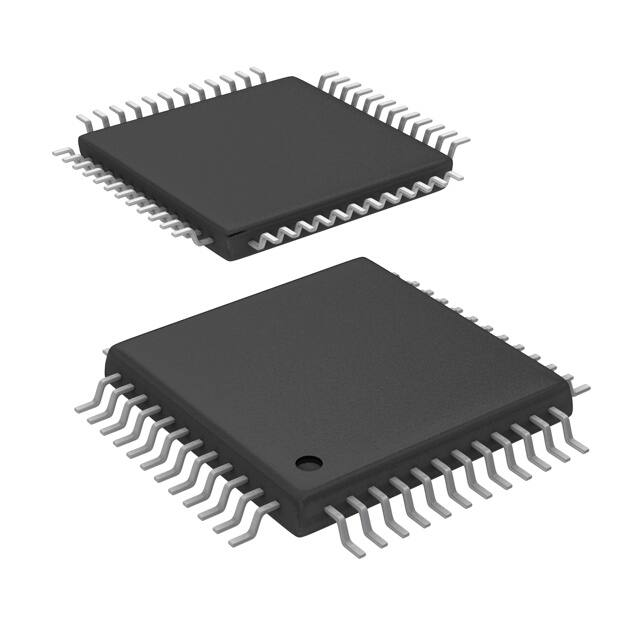
Package: 48-pin TQFP
The unbuffered voltage output offers low noise
performance (7 nV/√Hz) in combination with a fast
settling time (1µs), making this device an excellent
choice for low-noise, fast control-loop, and waveform
generation applications. The DACx1001 integrates an
enhanced deglitch circuit with code-independent
ultra-low glitch (1 nV-s) to enable clean waveform
ramps with ultra-low total harmonic distortion (THD).
The DACx1001 devices incorporate a power-on-reset
circuit so that the DAC powers with known values in
the registers. With external references, DAC output
ranges from VREFPF to VREFNF can be achieved,
including asymmetric output ranges.
2 Applications
•
•
•
•
•
•
•
•
•
Lab and field instrumentation
Spectrometer
Analog output module
Battery Test
Semiconductor test
Arbitrary waveform generator (AWG)
MRI
X-ray systems
Professional audio amplifier (rack mount)
The DACx1001 use a versatile 4–wire serial interface
that operates at clock rates of up to 50 MHz. The
DACx1001 is specified over the industrial
temperature range of –40°C to +125°C.
Device Information(1)
PART NUMBER
PACKAGE
BODY SIZE (NOM)
DAC11001A
DAC91001
TQFP (48)
7.00 mm × 7.00 mm
DAC81001
(1) For all available packages, see the package option addendum
at the end of the data sheet.
Functional Block Diagram
IOVDD DVDD
VCC
AVDD
High-Precision, Control-Loop Circuit
Gain/
Attenuation
REFPS REFPF
ROFS
LDAC
THS4011
Sensor
Output
REFPS
±
C1
RCM
±
REFNS
Power On Reset
±
RFB
Buffer
Registers
DACx1001
R
SPI Interface
SDO
+
REFPF
SDIN
SYNC
VREFP
R
SCLK
DAC
Register
DAC
+
THS4011
Power
Amplifier
Linear
Actuator
C2
REFNF
VREFN
+
THS4011
OUT
CLR
Power
Down Logic
ALARM
DGND
VSS
AGND
REFNS REFNF
1
An IMPORTANT NOTICE at the end of this data sheet addresses availability, warranty, changes, use in safety-critical applications,
intellectual property matters and other important disclaimers. PRODUCTION DATA.
�DAC11001A, DAC91001, DAC81001
SLASEL0B – OCTOBER 2019 – REVISED JUNE 2020
www.ti.com
Table of Contents
1
2
3
4
5
6
7
Features ..................................................................
Applications ...........................................................
Description .............................................................
Revision History.....................................................
Device Comparison Table.....................................
Pin Configuration and Functions .........................
Specifications.........................................................
1
1
1
2
3
3
5
7.1
7.2
7.3
7.4
7.5
7.6
Absolute Maximum Ratings ...................................... 5
ESD Ratings.............................................................. 5
Recommended Operating Conditions....................... 6
Thermal Information Package................................... 6
Electrical Characteristics........................................... 7
Timing Requirements: Write, 4.5 V ≤ DVDD ≤ 5.5
V............................................................................... 11
7.7 Timing Requirements: Write, 2.7 V ≤ DVDD < 4.5
V............................................................................... 12
7.8 Timing Requirements: Read and Daisy-Chain
Write, 4.5 V ≤ DVDD ≤ 5.5 V..................................... 13
7.9 Timing Requirements: Read and Daisy-Chain Write,
2.7 V ≤ DVDD < 4.5 V ............................................... 14
7.10 Typical Characteristics .......................................... 16
8
Detailed Description ............................................ 23
8.1 Overview ................................................................. 23
8.2 Functional Block Diagram ....................................... 23
8.3 Feature Description................................................. 23
8.4 Device Functional Modes........................................ 26
8.5 Programming........................................................... 27
8.6 Register Map........................................................... 29
9
Application and Implementation ........................ 34
9.1
9.2
9.3
9.4
9.5
Application Information............................................
Typical Application .................................................
System Examples ..................................................
What to Do and What Not to Do ............................
Initialization Set Up ................................................
34
34
39
42
42
10 Power Supply Recommendations ..................... 43
10.1 Power-Supply Sequencing.................................... 45
11 Layout................................................................... 46
11.1 Layout Guidelines ................................................. 46
11.2 Layout Example .................................................... 46
12 Device and Documentation Support ................. 47
12.1
12.2
12.3
12.4
12.5
12.6
12.7
12.8
Device Support......................................................
Documentation Support ........................................
Related Links ........................................................
Receiving Notification of Documentation Updates
Support Resources ...............................................
Trademarks ...........................................................
Electrostatic Discharge Caution ............................
Glossary ................................................................
47
47
47
47
47
47
47
47
13 Mechanical, Packaging, and Orderable
Information ........................................................... 48
4 Revision History
Changes from Revision A (December 2019) to Revision B
Page
•
Changed DAC81001 and DAC91001 from advanced information (preview) to production data (active), and added
associated content.................................................................................................................................................................. 1
•
Changed relative accuracy drift over time typical value from 0.1 LSB to ±0.1 LSB in Electrical Characteristics table ......... 7
•
Added output voltage drift over time parameter to the Electrical Characteristics table.......................................................... 8
•
Changed Figure 42, DAC Output Noise: 0.1 Hz to 10 Hz ................................................................................................... 22
Changes from Original (October 2019) to Revision A
•
2
Page
Changed DAC11001A device from advanced information (preview) to production data (active) .......................................... 1
Submit Documentation Feedback
Copyright © 2019–2020, Texas Instruments Incorporated
Product Folder Links: DAC11001A DAC91001 DAC81001
�DAC11001A, DAC91001, DAC81001
www.ti.com
SLASEL0B – OCTOBER 2019 – REVISED JUNE 2020
5 Device Comparison Table
DEVICE
RESOLUTION
DAC11001A
20-bit
DAC91001
18-bit
DAC81001
16-bit
6 Pin Configuration and Functions
NC
AGND
AGND
VCC
VSS
AGND
AGND
AVDD
AGND
AVDD
AGND
NC
48
47
46
45
44
43
42
41
40
39
38
37
PFB Package
48-Pin TQFP
Top View
REFPS
4
33
SYNC
REFNF
5
32
SDIN
REFNS
6
31
SCLK
OUT
7
30
CLR
AGND-OUT
8
29
NC
RFB
9
28
IOVDD
ROFS
10
27
DVDD
RCM
11
26
DGND
NC
12
25
NC
NC
DGND
DGND
DGND
DGND
ALARM
LDAC
DGND
DGND
NC
AGND-TnH
NC
Copyright © 2019–2020, Texas Instruments Incorporated
24
SDO
23
34
22
3
21
REFPF
20
AGND
19
35
18
2
17
AGND
16
NC
15
36
14
1
13
NC
Not to scale
Submit Documentation Feedback
Product Folder Links: DAC11001A DAC91001 DAC81001
3
�DAC11001A, DAC91001, DAC81001
SLASEL0B – OCTOBER 2019 – REVISED JUNE 2020
www.ti.com
Pin Functions
PIN
TYPE
DESCRIPTION
NAME
NO.
AGND
2, 35, 38,
40, 42, 43,
46, 47
Analog
ground
Connect to 0 V.
AGND-OUT
8
Analog
ground
Connect to 0 V. Measure DAC output voltage with respect to this node.
AGND-TnH
14
Analog
ground
Connect to 0 V. Integrated deglitcher clock ground..
ALARM
19
Output
Alarm output
39, 41
Power
Positive low voltage analog power supply
30
Input
DGND
16, 17, 20,
21, 22, 23,
26
Digital
ground
Connect to 0 V.
DVDD
27
Power
Digital power supply pin
RFB
9
Input
IOVDD
28
Power
Interface power supply pin
LDAC
18
Input
Load DAC pin, active low
1, 12, 13,
15, 24, 25,
29, 36, 37,
48
—
OUT
7
Output
RCM
11
Input
Integrated precision resistor common-mode node
REFNF
5
Input
External negative reference input. Connect to 0 V for unipolar DAC output.
REFNS
6
Input
External negative reference sense node
REFPF
3
Input
External positive reference input
REFPS
4
Input
External positive reference sense node
ROFS
10
Input
Integrated precision resistor offset node
SCLK
31
Input
Serial clock input of serial peripheral interface (SPI). Schmitt-trigger logic input.
Data are transferred at rates of up to 50 MHz.
SDIN
32
Input
Serial data input. Schmitt-trigger logic input.
Data are clocked into the input shift register on the falling edge of the serial clock input.
SDO
34
Output
SYNC
33
Input
VCC
45
Power
Analog positive power supply
VSS
44
Power
Analog negative power supply
AVDD
CLR
NC
4
DAC registers clear pin, active low
Integrated precision resistor feedback node
No connection, leave floating
Unbuffered voltage output
Serial data output. Data are valid on the falling edge of SCLK.
SPI bus chip select input (active low). Data bits are not clocked into the serial shift register unless
SYNC is low. When SYNC is high, the SDO pin is in high-impedance status.
Submit Documentation Feedback
Copyright © 2019–2020, Texas Instruments Incorporated
Product Folder Links: DAC11001A DAC91001 DAC81001
�DAC11001A, DAC91001, DAC81001
www.ti.com
SLASEL0B – OCTOBER 2019 – REVISED JUNE 2020
7 Specifications
7.1 Absolute Maximum Ratings
over operating free-air temperature range (unless otherwise noted) (1)
Positive supply voltage
Negative supply voltage
Positive reference voltage
Negative reference voltage
Digital and IO power supply
MIN
MAX
AVDD to AGND
–0.3
7
VCC to VSS
–0.3
40
VCC to AGND
–0.3
40
VSS to AGND
–19
0.3
VREFPF to VREFNF
–0.3
40
VREFPF to VCC
–0.3
VCC + 0.3
VREFPF to AGND
–0.3
40
–19
0.3
VSS – 0.3
0.3
VREFNF to AGND
VREFNF to VSS
DVDD, IOVDD to DGND
V
V
V
V
–0.3
7
V
DGND – 0.3
IOVDD + 0.3
V
VSS
VCC
0
VCC
Alarm pin voltage, ALARM to DGND
–0.3
DVDD + 0.3
Digital output, SDO to DGND
–0.3
DVDD + 0.3
Current into any pin
–10
10
mA
150
°C
150
°C
Digital input(s) to DGND
to AGND (VSS = AGND)
VOUT, VRFB, VRCM, VROFS
TJ
Junction temperature
Tstg
Storage temperature
(1)
UNIT
to VSS
–65
V
V
V
Stresses beyond those listed under Absolute Maximum Ratings may cause permanent damage to the device. These are stress ratings
only, which do not imply functional operation of the device at these or any other conditions beyond those indicated under Recommended
Operating Conditions. Exposure to absolute-maximum-rated conditions for extended periods may affect device reliability.
7.2 ESD Ratings
VALUE
V(ESD)
(1)
(2)
Electrostatic
discharge
Human body model (HBM), per ANSI/ESDA/JEDEC JS-001, all
pins (1)
±1000
Charged device model (CDM), per JEDEC specification
JESD22-C101, all pins (2)
±250
UNIT
V
JEDEC document JEP155 states that 500-V HBM allows safe manufacturing with a standard ESD control process.
JEDEC document JEP157 states that 250-V CDM allows safe manufacturing with a standard ESD control process.
Copyright © 2019–2020, Texas Instruments Incorporated
Submit Documentation Feedback
Product Folder Links: DAC11001A DAC91001 DAC81001
5
�DAC11001A, DAC91001, DAC81001
SLASEL0B – OCTOBER 2019 – REVISED JUNE 2020
www.ti.com
7.3 Recommended Operating Conditions
over operating free-air temperature range (unless otherwise noted)
MIN
NOM
UNIT
AVDD to AGND
4.5
5.5
V
VSS to AGND
–18
–3
V
VCC to AGND
8
33
V
VCC to VSS
11
36
V
DVDD to DGND
2.7
5.5
V
IOVDD to DGND
1.7
5.5
V
AGND to DGND
–0.3
0.3
V
VIH digital input high voltage
0.7 × IOVDD
V
VIL digital input low voltage
TA
MAX
0.3 × IOVDD
V
15
V
V
VREFPF to AGND
3
VREFNF to AGND
–15
0
VREFPF to VREFNF
3
30
V
–40
125
°C
Operating temperature
7.4 Thermal Information Package
THERMAL METRIC (1)
DAC11001A, DAC91001,
DAC81001
PFB (TQFP)
UNIT
48 PINS
RθJA
Junction-to-ambient thermal resistance
51.0
°C/W
RθJC(top)
Junction-to-case (top) thermal resistance
10.3
°C/W
RθJB
Junction-to-board thermal resistance
16.2
°C/W
ΨJT
Junction-to-top characterization parameter
0.3
°C/W
ΨJB
Junction-to-board characterization parameter
16.0
°C/W
RθJC(bot)
Junction-to-case (bottom) thermal resistance
N/A
°C/W
(1)
6
For more information about traditional and new thermal metrics, see the Semiconductor and IC Package Thermal Metrics application
report.
Submit Documentation Feedback
Copyright © 2019–2020, Texas Instruments Incorporated
Product Folder Links: DAC11001A DAC91001 DAC81001
�DAC11001A, DAC91001, DAC81001
www.ti.com
SLASEL0B – OCTOBER 2019 – REVISED JUNE 2020
7.5 Electrical Characteristics
at TA = –40°C to +125°C, VCC = +15 V, VSS = –15 V, AVDD = 5.5 V, DVDD = 3.3 V, IOVDD = 1.8 V, see note (1) for VREFPF and
VREFNF, 20-bit orderable used, OUT pin buffered with unity gain OPA827, ROFS, RCM, RFB unconnected, and all typical
specifications at TA = 25°C, (unless otherwise noted)
PARAMETER
TEST CONDITIONS
MIN
TYP
MAX
UNIT
STATIC PERFORMANCE
Resolution
DAC11001A
20
DAC91001
18
DAC81001
16
DAC11001A
DAC11001A
Relative accuracy (2)
INL
Relative accuracy drift over time
DNL
(2)
(3) (4)
–4
4
–2.6
2.6
DAC11001A, TA = 25°C (4)
–2
2
DAC91001
–1
1
DAC81001
–1
1
TA = 25°C, 1000 hrs
1
DAC11001A, TA = 0°C to 70°C, code 0d
into DAC, unipolar ranges only
–4
4
DAC11001A, TA = –40°C to +125°C,
code 0d into DAC, unipolar ranges only
–4
4
(1)
(2)
(3)
(4)
LSB
–4
4
DAC81001, TA = –40°C to +125°C, code
0d into DAC, unipolar ranges only
–4
4
TA = 0°C to 70°C, code 0d into DAC,
unipolar ranges only
±0.04
TA = –40°C to +125°C, code 0d into
DAC, unipolar ranges only
±0.04
ppm
FSR/°C
DAC11001A, TA = 0°C to 70°C
–8
8
DAC11001A, TA = 0°C to 70°C,
VREFPF = 3 V, VREFNF = –10 V
–8
8
–10
10
DAC11001A, TA = 25°C
Gain error temperature coefficient
LSB
±2
DAC91001, TA = –40°C to +125°C, code
0d into DAC, unipolar ranges only
DAC11001A, TA = –40°C to +125°C
Gain error (2) (4)
LSB
–1
DAC11001A, TA = 25°C, unipolar ranges
only
Zero code error temperature coefficient
LSB
±0.1
Differential nonlinearity (2) (3)
Zero code error (4)
Bits
±2
DAC91001, TA = –40°C to +125°C
–10
DAC81001, TA = –40°C to +125°C
–10
ppm of
FSR
10
10
TA = 0°C to 70°C
±0.04
TA = 0°C to 70°C, VREFPF = 3 V,
VREFNF = –10 V
±0.04
TA = –40°C to +125°C
±0.04
ppm
FSR/°C
Specified for the following pairs: VREFPF = 5 V and VREFNF = 0 V; VREFPF = 10 V and VREFNF = 0 V; VREFPF = +5 V and VREFNF = –5 V;
VREFPF = +10 V and VREFNF = –10 V.
Calculated between code 0d to 1048575d for DAC11001A, code 0d to 262143d for DAC91001, code 0d to 65535d for DAC81001.
With device temperature calibration mode enabled and used.
Specified by design, not production tested.
Copyright © 2019–2020, Texas Instruments Incorporated
Submit Documentation Feedback
Product Folder Links: DAC11001A DAC91001 DAC81001
7
�DAC11001A, DAC91001, DAC81001
SLASEL0B – OCTOBER 2019 – REVISED JUNE 2020
www.ti.com
Electrical Characteristics (continued)
at TA = –40°C to +125°C, VCC = +15 V, VSS = –15 V, AVDD = 5.5 V, DVDD = 3.3 V, IOVDD = 1.8 V, see note(1) for VREFPF and
VREFNF, 20-bit orderable used, OUT pin buffered with unity gain OPA827, ROFS, RCM, RFB unconnected, and all typical
specifications at TA = 25°C, (unless otherwise noted)
PARAMETER
TEST CONDITIONS
Positive full-scale error (4)
MIN
MAX
–8
8
DAC11001A, TA = 0°C to 70°C, code
1048575d into DAC, VREFPF = 3 V,
VREFNF = –10 V
–6
6
DAC11001A, TA = –40°C to +125°C,
code 1048575d into DAC
–10
10
DAC11001A, TA = 25°C, code 1048575d
into DAC
Full-scale error temperature coefficient
TYP
DAC11001A, TA = 0°C to 70°C, code
1048575d into DAC
UNIT
LSB
±2
DAC91001, TA = –40°C to +125°C, code
262143d into DAC
–10
10
DAC81001, TA = –40°C to +125°C, code
65535d into DAC
–10
10
TA = 0°C to 70°C
±0.04
TA = 0°C to 70°C, VREFPF = 3 V,
VREFNF = –10 V
±0.04
TA = –40°C to +125°C
±0.04
ppm
FSR/°C
OUTPUT CHARACTERISTICS
Headroom
From VREFPF to VCC
3
V
Footroom
From VREFNF to VSS
3
V
DC impedance
ZO
From ROFS to RCM
5
From RCM to RFB
5
DC output impedance
2.5
Power supply rejection ratio (dc)
Output voltage drift over time
TA = 25°C, VCC = 15 V ± 20%,
VSS = –15 V
kΩ
kΩ
1.5
µV/V
TA = 25°C, VCC = 15 V,
VSS = –15 V ± 20%
1
TA = 25°C, VOUT = midscale, 1000 hr
1
ppm of
FSR
VOLTAGE REFERENCE INPUT
8
Reference input impedance (REFPF)
DAC at midscale, VREFPF = 10 V,
VREFNF = 0 V
5.5
Reference input impedance (REFNF)
DAC at midscale, VREFPF = 10 V,
VREFNF = 0 V
7
Submit Documentation Feedback
kΩ
Copyright © 2019–2020, Texas Instruments Incorporated
Product Folder Links: DAC11001A DAC91001 DAC81001
�DAC11001A, DAC91001, DAC81001
www.ti.com
SLASEL0B – OCTOBER 2019 – REVISED JUNE 2020
Electrical Characteristics (continued)
at TA = –40°C to +125°C, VCC = +15 V, VSS = –15 V, AVDD = 5.5 V, DVDD = 3.3 V, IOVDD = 1.8 V, see note(1) for VREFPF and
VREFNF, 20-bit orderable used, OUT pin buffered with unity gain OPA827, ROFS, RCM, RFB unconnected, and all typical
specifications at TA = 25°C, (unless otherwise noted)
PARAMETER
TEST CONDITIONS
MIN
TYP
MAX
UNIT
DYNAMIC PERFORMANCE
VREFPF = 10 V, VREFNF = 0 V,
full-scale settling to 0.1%FSR
1
VREFPF = 10 V, VREFNF = 0 V,
full-scale settling to ±1 LSB
2.5
VREFPF = 10 V, VREFNF = 0 V,
1-mV step settling to ±1 LSB
2.5
Slew rate
VREFPF = 10 V, VREFNF = 0 V, full-scale
step, measured at OUT pin
50
Power-on glitch magnitude
Measured at unbuffered DAC voltage
output, VREFPF = 10 V, VREFNF = 0 V
Output voltage settling time (5)
ts
SR
Vn
V
0.4
µVpp
100-kHz bandwidth, DAC at midscale,
VREFPF = 10 V, VREFNF = 0 V
3
µVrms
Measured at 1 kHz, 10 kHz, 100 kHz,
DAC at mid scale, VREFPF = 10 V,
VREFNF = 0 V
7
nV/√Hz
DAC update rate = 400 kHz, fOUT = 1
kHz, VOUTPP = 0 V to 10 V
–105
dB
DAC update rate = 400 kHz, fOUT = 1
kHz, VOUTPP = 3 V to –10 V
–105
dB
DAC update rate = 400 kHz, fOUT = 1
kHz, VOUTPP = 0 V to 10 V
–105
dB
DAC update rate = 400 kHz, fOUT = 1
kHz, VOUTPP = 3 V to –10 V
–105
dB
200-mV 50-Hz or 60-Hz sine wave
superimposed on VSS, VCC = 15 V
95
dB
200-mV 50 Hz or 60 Hz sine wave
superimposed on VCC, VSS = –15 V
95
dB
Code change glitch impulse
±1 LSB change around mid code
(including feedthrough), VREFPF = 10 V,
VREFNF = 0 V, measured at output of
buffer op amp
1
nV-s
Code change glitch impulse magnitude
±1 LSB change around mid code
(including feedthrough), VREFPF = 10 V,
VREFNF = 0 V, measured at output of
buffer op amp
5
mV
Reference feedthrough
VREFPF = 10 V ± 10%, VREFNF = 0 V,
frequency = 100 Hz, DAC at zero scale
–90
dB
Reference feedthrough
VREFNF = –10 V ± 10%, VREFPF = 10 V,
frequency = 100 Hz, DAC at full scale
–90
dB
Digital feedthrough
At SCLK = 1 MHz, DAC output static at
midscale, 10-V range
1
0.1-Hz to 10-Hz, DAC at midscale,
VREFPF = 10 V, VREFNF = 0 V
Output noise density
THD
Spurious free dynamic range
Total harmonic distortion
Power supply rejection ratio (ac)
(5)
V/µs
–0.2
Output noise
SFDR
µs
nV-s
Adaptive TnH mode. TnH action is disabled for large code steps. For small steps, TnH action happens with a hold time of 1.2µs.
Copyright © 2019–2020, Texas Instruments Incorporated
Submit Documentation Feedback
Product Folder Links: DAC11001A DAC91001 DAC81001
9
�DAC11001A, DAC91001, DAC81001
SLASEL0B – OCTOBER 2019 – REVISED JUNE 2020
www.ti.com
Electrical Characteristics (continued)
at TA = –40°C to +125°C, VCC = +15 V, VSS = –15 V, AVDD = 5.5 V, DVDD = 3.3 V, IOVDD = 1.8 V, see note(1) for VREFPF and
VREFNF, 20-bit orderable used, OUT pin buffered with unity gain OPA827, ROFS, RCM, RFB unconnected, and all typical
specifications at TA = 25°C, (unless otherwise noted)
PARAMETER
TEST CONDITIONS
MIN
TYP
MAX
UNIT
DIGITAL INPUTS
Hysteresis voltage
Input current
Pin capacitance
Per pin
0.4
V
±5
µA
10
pF
DIGITAL OUTPUTS
VOL
Output low voltage
VOH
sinking 200 µA
Output high voltage
0.4
IOVDD –
0.5
sourcing 200 µA
V
V
High impedance leakage
±5
µA
High impedance output capacitance
10
pF
POWER
IAVDD
Current flowing into AVDD
VREFPF = 10 V, VREFNF = 0 V, midscale
code
1.5
mA
IVCC
Current flowing into VCC
VREFPF = 10 V, VREFNF = 0 V, midscale
code
7
mA
IVSS
Current flowing into VSS
VREFPF = 10 V, VREFNF = 0 V, midscale
code
7
mA
IDVDD
Current flowing into DVDD
VREFPF = 10 V, VREFNF = 0 V, midscale
code
0.5
mA
IIOVDD
Current flowing into IOVDD
VREFPF = 10 V, VREFNF = 0 V, midscale
code, all digital input pins static at IOVDD
0.1
mA
IREFPF
Reference input current (VREFPF)
VREFPF = 10 V, VREFNF = 0 V, midscale
code
5
mA
IREFNF
Reference input current (VREFNF)
VREFPF = 10 V, VREFNF = 0 V, midscale
code
5
mA
10
Submit Documentation Feedback
Copyright © 2019–2020, Texas Instruments Incorporated
Product Folder Links: DAC11001A DAC91001 DAC81001
�DAC11001A, DAC91001, DAC81001
www.ti.com
SLASEL0B – OCTOBER 2019 – REVISED JUNE 2020
7.6 Timing Requirements: Write, 4.5 V ≤ DVDD ≤ 5.5 V
all input signals are specified with tR = tF = 1 ns/V (10% to 90% of IOVDD) and timed from a voltage level of (VIL + VIH) / 2,
SDO loaded with 20 pF, and TA = –40°C to +125°C (unless otherwise noted)
MIN
fSCLK
tSCLKHIGH
tSCLKLOW
tSDIS
tSDIH
tCSS
tCSH
tCSHIGH
tCSIGNORE
tLDACSL
tLDACW
tCLRW
NOM
MAX
SCLK frequency, 1.7 V ≤ IOVDD < 2.7 V
33
SCLK frequency, 2.7 V ≤ IOVDD ≤ 5.5 V
50
SCLK high time, 1.7 V ≤ IOVDD < 2.7 V
15
SCLK high time, 2.7 V ≤ IOVDD ≤ 5.5 V
10
SCLK low time, 1.7 V ≤ IOVDD < 2.7 V
15
SCLK low time, 2.7 V ≤ IOVDD ≤ 5.5 V
10
SDI setup, 1.7 V ≤ IOVDD < 2.7 V
13
SDI setup, 2.7 V ≤ IOVDD ≤ 5.5 V
8
SDI hold, 1.7 V ≤ IOVDD < 2.7 V
13
SDI hold, 2.7 V ≤ IOVDD ≤ 5.5 V
8
SYNC falling edge to SCLK falling edge, 1.7 V ≤ IOVDD < 2.7 V
23
SYNC falling edge to SCLK falling edge, 2.7 V ≤ IOVDD ≤ 5.5 V
18
SCLK falling edge to SYNC rising edge, 1.7 V ≤ IOVDD < 2.7 V
15
SCLK falling edge to SYNC rising edge, 2.7 V ≤ IOVDD ≤ 5.5 V
10
SYNC high time, 1.7 V ≤ IOVDD < 2.7 V
55
SYNC high time, 2.7 V ≤ IOVDD ≤ 5.5 V
50
SCLK falling edge to SYNC ignore, 1.7 V ≤ IOVDD < 2.7 V
10
SCLK falling edge to SYNC ignore, 2.7 V ≤ IOVDD ≤ 5.5 V
5
Synchronous update: SYNC rising edge to LDAC falling edge, 1.7 V ≤
IOVDD < 2.7 V
50
Synchronous update: SYNC rising edge to LDAC falling edge, 2.7 V ≤
IOVDD ≤ 5.5 V
50
LDAC low time, 1.7 V ≤ IOVDD < 2.7 V
20
LDAC low time, 2.7 V ≤ IOVDD ≤ 5.5 V
20
CLR low time, 1.7 V ≤ IOVDD < 2.7 V
20
CLR low time, 2.7 V ≤ IOVDD ≤ 5.5 V
20
Copyright © 2019–2020, Texas Instruments Incorporated
UNIT
MHz
ns
ns
ns
ns
ns
ns
ns
ns
ns
Submit Documentation Feedback
Product Folder Links: DAC11001A DAC91001 DAC81001
ns
ns
11
�DAC11001A, DAC91001, DAC81001
SLASEL0B – OCTOBER 2019 – REVISED JUNE 2020
www.ti.com
7.7 Timing Requirements: Write, 2.7 V ≤ DVDD < 4.5 V
all input signals are specified with tR = tF = 1 ns/V (10% to 90% of IOVDD) and timed from a voltage level of (VIL + VIH) / 2,
SDO loaded with 20 pF, and TA = –40°C to +125°C (unless otherwise noted)
MIN
fSCLK
tSCLKHIGH
tSCLKLOW
tSDIS
tSDIH
tCSS
tCSH
tCSHIGH
tCSIGNORE
tLDACSL
tLDACW
tCLRW
12
NOM
MAX
SCLK frequency, 1.7 V ≤ IOVDD < 2.7 V
20
SCLK frequency, 2.7 V ≤ IOVDD ≤ 5.5 V
25
SCLK high time, 1.7 V ≤ IOVDD < 2.7 V
25
SCLK high time, 2.7 V ≤ IOVDD ≤ 5.5 V
20
SCLK low time, 1.7 V ≤ IOVDD < 2.7 V
25
SCLK low time, 2.7 V ≤ IOVDD ≤ 5.5 V
20
SDI setup, 1.7 V ≤ IOVDD < 2.7 V
21
SDI setup, 2.7 V ≤ IOVDD ≤ 5.5 V
16
SDI hold, 1.7 V ≤ IOVDD < 2.7 V
21
SDI hold, 2.7 V ≤ IOVDD ≤ 5.5 V
16
SYNC falling edge to SCLK falling edge, 1.7 V ≤ IOVDD < 2.7 V
41
SYNC falling edge to SCLK falling edge, 2.7 V ≤ IOVDD ≤ 5.5 V
36
SCLK falling edge to SYNC rising edge, 1.7 V ≤ IOVDD < 2.7 V
25
SCLK falling edge to SYNC rising edge, 2.7 V ≤ IOVDD ≤ 5.5 V
20
SYNC high time, 1.7 V ≤ IOVDD < 2.7 V
100
SYNC high time, 2.7 V ≤ IOVDD ≤ 5.5 V
100
SCLK falling edge to SYNC ignore, 1.7 V ≤ IOVDD < 2.7 V
10
SCLK falling edge to SYNC ignore, 2.7 V ≤ IOVDD ≤ 5.5 V
5
Synchronous update: SYNC rising edge to LDAC falling edge, 1.7 V ≤
IOVDD < 2.7 V
100
Synchronous update: SYNC rising edge to LDAC falling edge, 2.7 V ≤
IOVDD ≤ 5.5 V
100
MHz
ns
ns
ns
ns
ns
ns
ns
ns
ns
LDAC low time, 1.7 V ≤ IOVDD < 2.7 V
40
LDAC low time, 2.7 V ≤ IOVDD ≤ 5.5 V
40
CLR low time, 1.7 V ≤ IOVDD < 2.7 V
40
CLR low time, 2.7 V ≤ IOVDD ≤ 5.5 V
40
Submit Documentation Feedback
UNIT
ns
ns
Copyright © 2019–2020, Texas Instruments Incorporated
Product Folder Links: DAC11001A DAC91001 DAC81001
�DAC11001A, DAC91001, DAC81001
www.ti.com
SLASEL0B – OCTOBER 2019 – REVISED JUNE 2020
7.8 Timing Requirements: Read and Daisy-Chain Write, 4.5 V ≤ DVDD ≤ 5.5 V
all input signals are specified with tR = tF = 1 ns/V (10% to 90% of IOVDD) and timed from a voltage level of (VIL + VIH) / 2,
SDO loaded with 20 pF, and TA = –40°C to +125°C (unless otherwise noted)
MIN
fSCLK
tSCLKHIGH
tSCLKLOW
tSDIS
tSDIH
tCSS
tCSH
tCSHIGH
tCSIGNORE
tLDACSL
tLDACW
tCLRW
tSDODLY
tSDOZ
SCLK frequency
SCLK high time
SCLK low time
NOM
MAX
1.7 V ≤ IOVDD < 2.7 V, FSDO = 0
10
1.7 V ≤ IOVDD < 2.7 V, FSDO = 1
20
2.7 V ≤ IOVDD ≤ 5.5 V, FSDO = 0
15
2.7 V ≤ IOVDD ≤ 5.5 V, FSDO = 1
30
1.7 V ≤ IOVDD < 2.7 V, FSDO = 0
50
1.7 V ≤ IOVDD < 2.7 V, FSDO = 1
25
2.7 V ≤ IOVDD ≤ 5.5 V, FSDO = 0
33
2.7 V ≤ IOVDD ≤ 5.5 V, FSDO = 1
16
1.7 V ≤ IOVDD < 2.7 V, FSDO = 0
50
1.7 V ≤ IOVDD < 2.7 V, FSDO = 1
25
2.7 V ≤ IOVDD ≤ 5.5 V, FSDO = 0
33
2.7 V ≤ IOVDD ≤ 5.5 V, FSDO = 1
16
SDI setup, 1.7 V ≤ IOVDD < 2.7 V
13
SDI setup, 2.7 V ≤ IOVDD ≤ 5.5 V
8
SDI hold, 1.7 V ≤ IOVDD < 2.7 V
13
SDI hold, 2.7 V ≤ IOVDD ≤ 5.5 V
8
SYNC falling edge to SCLK falling edge, 1.7 V ≤ IOVDD < 2.7 V
30
SYNC falling edge to SCLK falling edge, 2.7 V ≤ IOVDD ≤ 5.5 V
20
SCLK falling edge to SYNC rising edge, 1.7 V ≤ IOVDD < 2.7 V
15
SCLK falling edge to SYNC rising edge, 2.7 V ≤ IOVDD ≤ 5.5 V
10
SYNC high time, 1.7 V ≤ IOVDD < 2.7 V
55
SYNC high time, 2.7 V ≤ IOVDD ≤ 5.5 V
50
SCLK falling edge to SYNC ignore, 1.7 V ≤ IOVDD < 2.7 V
10
SCLK falling edge to SYNC ignore, 2.7 V ≤ IOVDD ≤ 5.5 V
5
Synchronous update: SYNC rising edge to LDAC falling edge, 1.7 V ≤ IOVDD <
2.7 V
50
Synchronous update: SYNC rising edge to LDAC falling edge, 2.7 V ≤ IOVDD ≤
5.5 V
50
LDAC low time, 1.7 V ≤ IOVDD < 2.7 V
20
LDAC low time, 2.7 V ≤ IOVDD ≤ 5.5 V
20
CLR low time, 1.7 V ≤ IOVDD < 2.7 V
20
CLR low time, 2.7 V ≤ IOVDD ≤ 5.5 V
20
MHz
ns
ns
ns
ns
ns
ns
ns
ns
ns
ns
ns
SCLK rising edge to SDO valid data, 1.7 V ≤ IOVDD < 2.7 V, FSDO = 0
0
35
SCLK rising edge to SDO valid data, 2.7 V ≤ IOVDD ≤ 5.5 V, FSDO = 0
0
25
SCLK falling edge to SDO valid data, 1.7 V ≤ IOVDD < 2.7 V, FSDO = 1
0
35
SCLK falling edge to SDO valid data, 2.7 V ≤ IOVDD ≤ 5.5 V, FSDO = 1
0
25
SYNC rising edge to SDO HiZ, 1.7 V ≤ IOVDD < 2.7 V
0
20
SYNC rising edge to SDO HiZ, 2.7 V ≤ IOVDD ≤ 5.5 V
0
20
Copyright © 2019–2020, Texas Instruments Incorporated
UNIT
Submit Documentation Feedback
Product Folder Links: DAC11001A DAC91001 DAC81001
ns
ns
13
�DAC11001A, DAC91001, DAC81001
SLASEL0B – OCTOBER 2019 – REVISED JUNE 2020
www.ti.com
7.9 Timing Requirements: Read and Daisy-Chain Write, 2.7 V ≤ DVDD < 4.5 V
all input signals are specified with tR = tF = 1 ns/V (10% to 90% of IOVDD) and timed from a voltage level of (VIL + VIH) / 2,
SDO loaded with 20 pF, and TA = –40°C to +125°C (unless otherwise noted)
MIN
fSCLK
SCLK frequency
tSCLKHIGH
tSCLKLOW
tSDIS
tSDIH
tCSS
tCSH
tCSHIGH
tCSIGNORE
tLDACSL
tLDACW
tCLRW
tSDODLY
tSDOZ
14
SCLK high time
SCLK low time
NOM
MAX
1.7 V ≤ IOVDD < 2.7 V, FSDO = 0
8
1.7 V ≤ IOVDD < 2.7 V, FSDO = 1
16
2.7 V ≤ IOVDD ≤ 5.5 V, FSDO = 0
10
2.7 V ≤ IOVDD ≤ 5.5 V, FSDO = 1
20
1.7 V ≤ IOVDD < 2.7 V, FSDO = 0
62
1.7 V ≤ IOVDD < 2.7 V, FSDO = 1
31
2.7 V ≤ IOVDD ≤ 5.5 V, FSDO = 0
50
2.7 V ≤ IOVDD ≤ 5.5 V, FSDO = 1
25
1.7 V ≤ IOVDD < 2.7 V, FSDO = 0
62
1.7 V ≤ IOVDD < 2.7 V, FSDO = 1
31
2.7 V ≤ IOVDD ≤ 5.5 V, FSDO = 0
50
2.7 V ≤ IOVDD ≤ 5.5 V, FSDO = 1
25
SDI setup, 1.7 V ≤ IOVDD < 2.7 V
21
SDI setup, 2.7 V ≤ IOVDD ≤ 5.5 V
16
SDI hold, 1.7 V ≤ IOVDD < 2.7 V
21
SDI hold, 2.7 V ≤ IOVDD ≤ 5.5 V
16
SYNC falling edge to SCLK falling edge, 1.7 V ≤ IOVDD < 2.7 V
41
SYNC falling edge to SCLK falling edge, 2.7 V ≤ IOVDD ≤ 5.5 V
36
SCLK falling edge to SYNC rising edge, 1.7 V ≤ IOVDD < 2.7 V
25
SCLK falling edge to SYNC rising edge, 2.7 V ≤ IOVDD ≤ 5.5 V
20
SYNC high time, 1.7 V ≤ IOVDD < 2.7 V
100
SYNC high time, 2.7 V ≤ IOVDD ≤ 5.5 V
100
SCLK falling edge to SYNC ignore, 1.7 V ≤ IOVDD < 2.7 V
10
SCLK falling edge to SYNC ignore, 2.7 V ≤ IOVDD ≤ 5.5 V
5
Synchronous update: SYNC rising edge to LDAC falling edge, 1.7 V ≤ IOVDD <
2.7 V
100
Synchronous update: SYNC rising edge to LDAC falling edge, 2.7 V ≤ IOVDD ≤
5.5 V
100
MHz
ns
ns
ns
ns
ns
ns
ns
ns
ns
LDAC low time, 1.7 V ≤ IOVDD < 2.7 V
40
LDAC low time, 2.7 V ≤ IOVDD ≤ 5.5 V
40
CLR low time, 1.7 V ≤ IOVDD < 2.7 V
40
CLR low time, 2.7 V ≤ IOVDD ≤ 5.5 V
40
ns
ns
SCLK rising edge to SDO valid data, 1.7 V ≤ IOVDD < 2.7 V, FSDO = 0
0
40
SCLK rising edge to SDO valid data, 2.7 V ≤ IOVDD ≤ 5.5 V, FSDO = 0
0
30
SCLK rising edge to SDO valid data, 1.7 V ≤ IOVDD < 2.7 V, FSDO = 1
0
40
SCLK rising edge to SDO valid data, 2.7 V ≤ IOVDD ≤ 5.5 V, FSDO = 1
0
30
SYNC rising edge to SDO HiZ, 1.7 V ≤ IOVDD < 2.7 V
0
20
SYNC rising edge to SDO HiZ, 2.7 V ≤ IOVDD ≤ 5.5 V
0
20
Submit Documentation Feedback
UNIT
ns
ns
Copyright © 2019–2020, Texas Instruments Incorporated
Product Folder Links: DAC11001A DAC91001 DAC81001
�DAC11001A, DAC91001, DAC81001
www.ti.com
SLASEL0B – OCTOBER 2019 – REVISED JUNE 2020
tCSS
tCSHIGH
tCSH
SYNC
tCSIGNORE
tSCLKLOW
SCLK
tSCLKHIGH
tSDIS
SDIN
tSDIH
Bit 31
Bit 1
Bit 0
LDAC1
tCLRW
tLDACSL
tLDACW
CLR
Figure 1. Serial Interface Write Timing: Standalone Mode
tCSHIGH
tCSS
tCSH
SYNC
tCSIGNOR
E
tSCLKLOW
SCLK
tSCLKHIGH
FIRST READ COMMAND
SDIN
Bit 31
tSDIS
Bit 22
ANY COMMAND
Bit 0
Bit 31
Bit 22
Bit 0
tSDIH
DATA FROM FIRST
READ COMMAND
SDO
Bit 31
Bit 22
Bit 0
tSDODZ
tSDODLY
LDAC
1
tCLRW
tLDACSL
tLDACW
CLR
Figure 2. Serial Interface Read and Write Timing: Daisy-Chain Mode
Copyright © 2019–2020, Texas Instruments Incorporated
Submit Documentation Feedback
Product Folder Links: DAC11001A DAC91001 DAC81001
15
�DAC11001A, DAC91001, DAC81001
SLASEL0B – OCTOBER 2019 – REVISED JUNE 2020
www.ti.com
7.10 Typical Characteristics
4
1
3
0.8
2
1
0
-1
-2
UP, 5 V
UP, 10 V
BP, ±10 V
UP, 10 V (gain = 2x)
-3
Differential Linearity Error (LSB)
Integral Linearity Error (LSB)
at TA = 25°C, VCC = 15 V, VSS = –15 V, AVDD = 5 V, IOVDD = 1.8 V, gain resistors unconnected (gain = 1x), OPA827 used as
output and reference amplifier, UP = unipolar, BP = bipolar, and temperature calibration disabled (unless otherwise noted)
0.6
0.4
0.2
0
-0.2
-0.4
-0.8
-1
-4
0
262144
524288
Code
786432
0
1048575
Figure 3. . Integral Linearity Error vs Digital Input Code
1
3
0.8
2
1
0
-1
-2
-3
INL max, UP, 5 V
INL max, UP, 10 V
INL max, BP, ±10 V
INL min, UP, 5 V
-4
-40 -25 -10
5
INL min, UP, 10 V
INL min, BP, ±10 V
INL max, UP, 10 V, [gain 2x]
INL min, UP, 10 V, [gain 2x]
20 35 50 65
Temperature (°C)
80
95
262144
524288
Code
786432
1048575
Figure 4. Differential Linearity Error vs Digital Input Code
4
Differential Linearity Error (LSB)
Integral Linearity Error (LSB)
UP, 5 V
UP, 10 V
BP, ±10 V
UP, 10 V, [gain = 2x]
-0.6
0.6
0.4
0.2
0
-0.2
-0.4
-0.6
-0.8
DNL max, UP, 5 V
DNL max, UP, 10 V
DNL max, BP, ±10 V
DNL min, UP, 5 V
-1
-40 -25 -10
110 125
5
DNL min, UP, 10 V
DNL min, BP, ±10 V
DNL max, UP, 10 V [gain 2x]
DNL min, UP, 10 V [gain 2x]
20 35 50 65
Temperature (°C)
80
95
110 125
Temperature calibration enabled
3
8
2
1
0
-1
-2
-3
UP, 5 V
BP, ±5 V
-4
-40 -25 -10
5
20 35 50 65
Temperature (°C)
UP, 10 V
BP, ±10 V
80
95
110 125
Temperature calibration enabled
6
4
2
0
-2
-4
-6
UP, 5 V
BP, ±5 V
-8
-10
-40 -25 -10
5
20 35 50 65
Temperature (°C)
UP, 10 V
BP, ±10 V
80
95
110 125
Temperature calibration enabled
Figure 7. Zero Code Error vs Temperature
16
Figure 6. Differential Linearity Error vs Temperature
10
Positive Full-sale Error (LSB)
Zero Code Error (LSB)
Figure 5. Integral Linearity Error vs Temperature
4
Submit Documentation Feedback
Figure 8. Positive Full-Scale Error vs Temperature
Copyright © 2019–2020, Texas Instruments Incorporated
Product Folder Links: DAC11001A DAC91001 DAC81001
�DAC11001A, DAC91001, DAC81001
www.ti.com
SLASEL0B – OCTOBER 2019 – REVISED JUNE 2020
Typical Characteristics (continued)
15
4
12
3
Integral Linearity Error (LSB)
Gain Error (ppm of FSR)
at TA = 25°C, VCC = 15 V, VSS = –15 V, AVDD = 5 V, IOVDD = 1.8 V, gain resistors unconnected (gain = 1x), OPA827 used as
output and reference amplifier, UP = unipolar, BP = bipolar, and temperature calibration disabled (unless otherwise noted)
9
6
3
0
-3
-6
-9
UP, 5 V
BP, ±5 V
-12
-15
-40 -25 -10
5
20 35 50 65
Temperature (°C)
95
1
0
-1
-2
-3
UP, 10 V
BP, ±10 V
80
2
-4
11
110 125
INL min, UP, 5 V
INL max, UP, 5 V
11.5
INL min, BP, r5 V
INL max, BP, r5 V
12
12.5
13
13.5
14
Supply Voltage, VCC (V) = VSS (V)
14.5
15
Temperature calibration enabled
Figure 10. Integral Linearity Error vs Supply Voltage
10
0.8
8
0.6
6
Zero Code Error (LSB)
Differential Linearity Error (LSB)
Figure 9. Gain Error vs Temperature
1
0.4
0.2
0
-0.2
-0.4
-0.6
2
0
-2
-4
-6
DNL min, UP, 5 V
DNL max, UP, 5 V
-0.8
-1
11
4
11.5
DNL min, BP, r5 V
DNL max, BP, r5 V
12
12.5
13
13.5
14
Supply Voltage, VCC (V) = VSS (V)
14.5
-10
11
15
Figure 11. Differential Linearity Error vs Supply Voltage
12
12.5
13
13.5
14
Supply Voltage, VCC (V) = VSS (V)
14.5
15
4
BP, 5 V
UP, 5 V
3.2
2.4
1.6
0.8
0
-0.8
-1.6
-2.4
-3.2
BP, 5 V
UP, 5 V
3.2
Gain Error (ppm of FSR)
Positive Full Scale Error (LSB)
11.5
Figure 12. Zero Code Error vs Supply Voltage
4
-4
11
BP, r5 V
UP, 5 V
-8
2.4
1.6
0.8
0
-0.8
-1.6
-2.4
-3.2
11.5
12
12.5
13
13.5
14
Supply Voltage, VCC (V) = VSS (V)
14.5
15
Figure 13. Positive Full-Scale Error vs Supply Voltage
Copyright © 2019–2020, Texas Instruments Incorporated
-4
11
11.5
12
12.5
13
13.5
14
Supply Voltage, VCC (V) = VSS (V)
14.5
15
Figure 14. Gain Error vs Supply Voltage
Submit Documentation Feedback
Product Folder Links: DAC11001A DAC91001 DAC81001
17
�DAC11001A, DAC91001, DAC81001
SLASEL0B – OCTOBER 2019 – REVISED JUNE 2020
www.ti.com
Typical Characteristics (continued)
4
1
3
0.8
Differential Linearity Error (LSB)
Integral Linearity Error (LSB)
at TA = 25°C, VCC = 15 V, VSS = –15 V, AVDD = 5 V, IOVDD = 1.8 V, gain resistors unconnected (gain = 1x), OPA827 used as
output and reference amplifier, UP = unipolar, BP = bipolar, and temperature calibration disabled (unless otherwise noted)
2
1
0
-1
-2
-3
INL min
INL max
0.6
0.4
0.2
0
-0.2
-0.4
-0.6
-4
-1
5
5.5
6
6.5
7
7.5
8
8.5
9
9.5
Reference Voltage, VREFPF (V) = VREFNF (V)
10
5
Figure 15. Integral Linearity Error vs Reference Voltage
0
3.2
-0.2
2.4
-0.4
1.6
0.8
0
-0.8
-1.6
-2.4
5.5
6
6.5
7
7.5
8
8.5
9
9.5
Reference Voltage, VREFPF (V) = VREFNF (V)
-3.2
-0.6
-0.8
-1
-1.2
-1.4
-1.6
-1.8
-4
-2
5
5.5
6
6.5
7
7.5
8
8.5
9
9.5
Reference Voltage, VREFPF (V) = VREFNF (V)
10
5
Figure 17. Zero Code Error vs Reference Voltage
5.5
6
6.5
7
7.5
8
8.5
9
9.5
Reference Voltage, VREFPF (V) = VREFNF (V)
10
Figure 18. Gain Error vs Reference Voltage
1.5
20
IDVDD
IIOVDD
1.2
0.9
16
0.6
Current (PA)
Positive Full Scale Error (LSB)
10
Figure 16. Differential Linearity Error vs Reference Voltage
4
Gain Error (ppm of FSR)
Zero Code Error (LSB)
DNL min
DNL max
-0.8
0.3
0
-0.3
12
8
-0.6
-0.9
4
-1.2
-1.5
0
5
5.5
6
6.5
7
7.5
8
8.5
9
9.5
Reference Voltage, VREFPF (V) = VREFNF (V)
10
0
262144
524288
Code
786432
1048576
VREFPF = 10 V, VREFNF = 0 V
Figure 19. Positive Full-Scale Error vs Reference Voltage
18
Submit Documentation Feedback
Figure 20. Supply Current (DVDD and IOVDD)
vs Digital Input Code
Copyright © 2019–2020, Texas Instruments Incorporated
Product Folder Links: DAC11001A DAC91001 DAC81001
�DAC11001A, DAC91001, DAC81001
www.ti.com
SLASEL0B – OCTOBER 2019 – REVISED JUNE 2020
Typical Characteristics (continued)
at TA = 25°C, VCC = 15 V, VSS = –15 V, AVDD = 5 V, IOVDD = 1.8 V, gain resistors unconnected (gain = 1x), OPA827 used as
output and reference amplifier, UP = unipolar, BP = bipolar, and temperature calibration disabled (unless otherwise noted)
5
7
IREFPF
IIREFNF
5
3
1
IVCC
IIVSS
-1
Current (mA)
Current (mA)
3
1
-1
-3
-3
-5
-5
-7
0
262144
524288
Code
786432
0
1048576
VREFPF = 10 V, VREFNF = 0 V
262144
524288
Code
786432
1048576
VREFPF = 10 V, VREFNF = 0 V
Figure 21. Supply Current (VCC and VSS)
vs Digital Input Code
Figure 22. Reference Current (VREFPF and VREFNF)
vs Digital Input Code
2
50
IAVDD
IDVDD)
40
Current (PA)
Current (mA)
1.6
1.2
0.8
0.4
30
20
10
0
0
262144
524288
Code
786432
0
-40 -25 -10
1048576
VREFPF = 10 V, VREFNF = 0 V
5
20 35 50 65
Temperature (°C)
80
95
110 125
VREFPF = 10 V, VREFNF = 0 V, DAC at midcode
Figure 23. Supply Current (AVDD) vs Digital Input Code
Figure 24. Supply Current (DVDD) vs Temperature
8
12
IVCC
IVSS
8
IREFPF
IREFNF
6
Current (mA)
Current (mA)
4
4
0
-4
2
0
-2
-4
-8
-6
-12
-40 -25 -10
5
20 35 50 65
Temperature (°C)
80
95
110 125
VREFPF = 10 V, VREFNF = 0 V, DAC at midcode
Figure 25. Supply Current (VCC and VSS)
vs Temperature
Copyright © 2019–2020, Texas Instruments Incorporated
-8
-40 -25 -10
5
20 35 50 65
Temperature (°C)
80
95
110 125
VREFPF = 10 V, VREFNF = 0 V, DAC at midcode
Figure 26. Reference Current (VREFPF and VREFNF)
vs Temperature
Submit Documentation Feedback
Product Folder Links: DAC11001A DAC91001 DAC81001
19
�DAC11001A, DAC91001, DAC81001
SLASEL0B – OCTOBER 2019 – REVISED JUNE 2020
www.ti.com
Typical Characteristics (continued)
at TA = 25°C, VCC = 15 V, VSS = –15 V, AVDD = 5 V, IOVDD = 1.8 V, gain resistors unconnected (gain = 1x), OPA827 used as
output and reference amplifier, UP = unipolar, BP = bipolar, and temperature calibration disabled (unless otherwise noted)
12
2
IAVDD
1.8
8
1.6
4
Current (mA)
1.2
1
0.8
0
-4
0.6
0.4
-8
0.2
IVCC
0
-40 -25 -10
5
20 35 50 65
Temperature (°C)
80
95
-12
11
110 125
11.5
12
12.5
13
13.5
14
Supply Voltage, VCC (V) = VSS (V)
Figure 28. Supply Current (VCC and VSS) vs Supply Voltage
Figure 27. Supply Current (AVDD) vs Temperature
50
1000
IOVDD = 1.8 V
IOVDD = 5 V
IOVDD = 3 V
40
Current (PA)
Current (PA)
800
600
400
30
20
10
200
0
0
0
0.5
1
1.5
2
2.5
3
3.5
Logic Voltage, VLOGIC (V)
4
4.5
0
5
VREFPF = 10 V, VREFNF = 0 V, DAC at midcode
0.2
0.4
0.6
0.8
1
1.2
Logic Voltage, VLOGIC (V)
1.4
1.6
1.8
VREFPF = 10 V, VREFNF = 0 V, DAC at midcode
Figure 29. Supply Current (IOVDD)
vs Input Pin Logic Level
0.005
Figure 30. Supply Current (IOVDD = 1.8 V)
vs Input Pin Logic Level
15
VOUT
LDAC 10
0.004
0.005
15
VOUT
LDAC 10
0.004
0.003
5
0.003
5
0.002
0
0.002
0
0.001
-5
0.001
-5
LDAC Voltage (V)
Output Voltage (V)
Output Voltage (V)
15
VREFPF = 5 V, VREFNF = 0 V, DAC at midcode
VREFPF = 10 V, VREFNF = 0 V, DAC at midcode
0
-10
-0.001
-15
-0.002
-20
-0.003
-25
-0.003
-0.004
-30
-0.004
-35
5E-6
-0.005
DAC Glitch (0.75 nV-s)
-0.005
0
1E-6
2E-6
3E-6
Time (s)
4E-6
VREFPF = 10 V, VREFNF = –10 V, DAC transition midcode – 1 to
midcode
Figure 31. Glitch Impulse, Rising Edge, 1-LSB Step
20
IVSS
14.5
Submit Documentation Feedback
0
-10
-0.001
-15
-0.002
-20
LDAC Voltage (V)
Current (mA)
1.4
-25
DACV glitch (0.4 nV-s)
-30
0
1E-6
2E-6
3E-6
Time (s)
4E-6
-35
5E-6
VREFPF = 10 V, VREFNF = –10 V, DAC transition midcode to
midcode – 1
Figure 32. Glitch Impulse, Falling Edge, 1-LSB Step
Copyright © 2019–2020, Texas Instruments Incorporated
Product Folder Links: DAC11001A DAC91001 DAC81001
�DAC11001A, DAC91001, DAC81001
www.ti.com
SLASEL0B – OCTOBER 2019 – REVISED JUNE 2020
Typical Characteristics (continued)
at TA = 25°C, VCC = 15 V, VSS = –15 V, AVDD = 5 V, IOVDD = 1.8 V, gain resistors unconnected (gain = 1x), OPA827 used as
output and reference amplifier, UP = unipolar, BP = bipolar, and temperature calibration disabled (unless otherwise noted)
1.6
0.6
Code
983040
VREFPF = 10 V, VREFNF = 0 V
Figure 33. Segment Glitch Impulse, 1-LSB Step
Figure 34. Segment Glitch Impulse, 1-LSB Step
10.033
VOUT glitch, rise
VOUT glitch, fall
1.4
40
VOUT (zoomed)
Settling band (+0.1%)
Settling band ( 0.1%)
10.028
10.023
1.2
Voltage (V)
1
0.8
0.6
0.4
0.2
30
20
10.018
10
10.013
0
10.008
-10
10.003
-20
9.998
-30
9.993
-40
9.988
-50
1E-6 2E-6 3E-6 4E-6 5E-6 6E-6 7E-6 8E-6 9E-6 1E-5
Time(s)
0
1048575
983040
917504
851968
786432
720896
655360
589824
524288
458752
393216
327680
262144
196608
131072
0
0
VOUT
LDAC
Voltage (V)
1.6
65536
1048575
917504
720896
655360
589824
524288
458752
Code
VREFPF = 10 V, VREFNF = –10 V
DAC Output Glitch (nV-s)
393216
0
983040
1048575
917504
851968
786432
720896
655360
589824
524288
458752
393216
327680
0
262144
0
196608
0.2
131072
0.2
327680
0.4
262144
0.4
0.8
196608
0.6
1
131072
0.8
1.2
65536
DAC Output Glitch (nV-s)
1
0
VOUT glitch, rise
VOUT glitch, fall
1.4
1.2
65536
DAC Output Glitch (nV-s)
1.4
851968
VOUT glitch, rise
VOUT glitch, fall
786432
1.6
VREFPF = 10 V, VREFNF = 0 V
Code
VREFPF = 5 V, VREFNF = 0 V
0
VREFPF = 10 V, VREFNF = 0 V
0.0025
20
0.00245
10
0.0024
0
0.00235
-10
0.0023
-20
0.00225
-30
0.0022
-40
VOUT (zoomed)
Settling band (+1 LSB)
Settling band ( 1 LSB) -50
LDAC
-60
1E-6 2E-6 3E-6 4E-6 5E-6 6E-6 7E-6 8E-6 9E-6 1E-5
Time(s)
0.00215
0.0021
0
Voltage (V)
Figure 36. Full-Scale Settling Time, Rising Edge
Voltage (V)
45
VOUT (zoomed)
VOUT 42
Settling band (+0.1%)
LDAC 39
Settling band ( 0.1%)
36
33
30
27
24
21
18
15
12
9
6
3
0
-3
1E-6 2E-6 3E-6 4E-6 5E-6 6E-6 7E-6 8E-6 9E-6 1E-5
Time(s)
Voltage (V)
Voltage (V)
Figure 35. Segment Glitch Impulse, 1-LSB Step
0.012
0.01
0.008
0.006
0.004
0.002
0
-0.002
-0.004
-0.006
-0.008
-0.01
-0.012
-0.014
-0.016
-0.018
-0.02
VREFPF = 10 V, VREFNF = 0 V, DAC transitions 100 codes around
midscale
Figure 37. Full-Scale Settling Time, Falling Edge
Copyright © 2019–2020, Texas Instruments Incorporated
Figure 38. 100 Codes Settling Time, Rising Edge
Submit Documentation Feedback
Product Folder Links: DAC11001A DAC91001 DAC81001
21
�DAC11001A, DAC91001, DAC81001
SLASEL0B – OCTOBER 2019 – REVISED JUNE 2020
www.ti.com
Typical Characteristics (continued)
16
40
0.00125
8
0
0.0012
0
0.00115
-8
0.0011
-16
0.00105
0.001
0
VOUT (zoomed)
Settling band (+1 LSB) -24
Settling band ( 1 LSB)
LDAC
-32
1E-6 2E-6 3E-6 4E-6 5E-6 6E-6 7E-6 8E-6 9E-6 1E-5
Time(s)
VREFPF = 10 V, VREFNF = 0 V, DAC transitions 100 codes around
midscale
DAC Output THD+N (dB)
0.0013
Voltage (V)
Voltage (V)
at TA = 25°C, VCC = 15 V, VSS = –15 V, AVDD = 5 V, IOVDD = 1.8 V, gain resistors unconnected (gain = 1x), OPA827 used as
output and reference amplifier, UP = unipolar, BP = bipolar, and temperature calibration disabled (unless otherwise noted)
-40
-80
-120
-160
-200
100
7.75
7
6.25
5.5
24000
VOUT (0.1 PV/div)
Output Voltage Noise (PVPP)
Output Voltage Noise (nv/—Hz)
8.5
20100
Figure 40. Total Harmonic Distortion (THD + N)
vs Frequency
10
Zero code
Mid code
Full code
8100
12100
16100
Frequency (Hz)
VREFPF = 10 V, VREFNF = 0 V, DAC output frequency = 1 kHz,
DAC update rate = 400 kHz
Figure 39. 100 Codes Settling Time, Falling Edge
9.25
4100
4.75
1000
2000
5000 10000 20000
Frequency (Hz)
50000 100000
Time (1 s/div)
D037
VREFPF = 10 V, VREFNF = 0 V, DAC at midcode, measured at DAC
output pin
VREFPF = 10 V, VREFNF = 0 V, measured at DAC output
Figure 41. DAC Output Noise Spectral Density
Figure 42. DAC Output Noise: 0.1 Hz to 10 Hz
VOUT Voltage (V)
0.001
10
0.00075
5
0.0005
0
0.00025
-5
0
-10
-0.00025
-15
-0.0005
-20
-0.00075
VOUT -25
SCLK
-30
2E-6
-0.001
0
5E-7
1E-6
Time (s)
1.5E-6
SCLK Voltage (V)
4
500
VREFPF = 10 V, VREFNF = 0 V, DAC at midcode, measured at DAC output pin
Figure 43. Clock Feedthrough
22
Submit Documentation Feedback
Copyright © 2019–2020, Texas Instruments Incorporated
Product Folder Links: DAC11001A DAC91001 DAC81001
�DAC11001A, DAC91001, DAC81001
www.ti.com
SLASEL0B – OCTOBER 2019 – REVISED JUNE 2020
8 Detailed Description
8.1 Overview
The 20-bit DAC11001A, 18-bit DAC91001, and 16-bit DAC81001 (DACx1001) are single-channel DACs. The
unbuffered DAC output architecture is based on an R2R ladder that is designed to provide monotonicity over
wide reference and temperature ranges (1-LSB DNL). This architecture provides a very low-noise (7 nV/√Hz) and
fast-settling (1 µs) output. The DACx1001 also implement a deglitch circuit that enables low, code-independent
glitch at the DAC output. This is extremely useful for creating ultra low harmonic distortion waveform generation.
The DACx1001 requires external reference voltages on REFPF and REFNF pins. The output of the DAC ranges
from VREFNF to VREFPF. See the Recommended Operating Conditions for VREFPF and VREFNF voltage ranges.
The DACx1001 also includes precision matched gain setting pins (ROFS, RCM, and RFB), Using these pins and
an external op amp, the DAC output can be scaled. The DACx1001 incorporate a power-on-reset circuit that
makes sure that the DAC output powers up at zero scale, and remains at zero scale until a valid DAC command
is issued. The DACx1001 use a 4-wire serial interface that operates at clock rates of up to 50 MHz.
8.2 Functional Block Diagram
IOVDD DVDD
VCC
AVDD
REFPS REFPF
ROFS
R
SCLK
SDIN
SDO
LDAC
R
SPI Interface
SYNC
RCM
Power On Reset
RFB
Buffer
Registers
DAC
Register
DAC
OUT
CLR
Power
Down Logic
ALARM
DGND
VSS
AGND
REFNS REFNF
8.3 Feature Description
8.3.1 Digital-to-Analog Converter Architecture
The DACx1001 provide 20-bit monotonic outputs using an R2R ladder architecture. The DAC output ranges
between VREFNF and VREFPF based on the 20-bit DAC data, as described in Equation 1:
CODE
VOUT (VREFPF VREFNF ) u
VREFNF
2N
where
•
•
•
CODE is the decimal equivalent of the DAC-DATA loaded to the DAC.
N is the bits of resolution; 20 for DAC1101A, 18 for DAC91001, 16 for DAC81001.
VREFPF, VREFNF is the reference voltage (positive and negative).
Copyright © 2019–2020, Texas Instruments Incorporated
Submit Documentation Feedback
Product Folder Links: DAC11001A DAC91001 DAC81001
(1)
23
�DAC11001A, DAC91001, DAC81001
SLASEL0B – OCTOBER 2019 – REVISED JUNE 2020
www.ti.com
Feature Description (continued)
8.3.2 External Reference
The DACx1001 require external references (REFPF and REFNF) to operate. See the Recommended Operating
Conditions for VREFPF and VREFNF voltage ranges.
The DACx1001 also contain dedicated sense pins, REFPS for REFPF and REFNS for REFNF. The reference
pins are unbuffered; therefore, use a reference driver circuit for these pins. Set the VREFVAL bits (address 02h)
as per a reference span equal to (VREFPF – VREFNF). For example, the VREFVAL bits must be set to 0100 for
VREFPF = 5 V and VREFNF = –5 V.
Figure 44 shows an example reference drive circuit for DACx1001. Table 1 shows the op-amp options for the
reference driver circuit.
VREFP
+
Voltage
Reference
REFPF
±
C1
REFPS
ROFS
RCM
DACx1001
RFB
REFNS
±
C2
±
REFNF
+
±
DAC-OUT
VOUT
+
+
VREFN
Figure 44. Reference Drive Circuit
Table 1. Reference Op Amp Options
SELECTION PARAMETERS
OP AMPS
Low voltage and current noise
OPA211, OPA827, OPA828
Low offset and drift
OPA189
8.3.3 Output Buffers
The DACx1001 outputs are unbuffered. Use an external op amp to buffer the DAC output. The DAC output
voltage ranges from VREFPF to VREFNF. Two gain-setting resistors are integrated in the DACx1001. These
resistors are used to scale the DAC output, minimize the bias current mismatch of the external op amp, and
generate a negative reference for the REFNF pin. See the Embedded Resistor Configurations section for more
information. Table 2 shows the op amp options for the output drive circuit.
Table 2. Output Op Amp Options
24
SELECTION PARAMETERS
OP AMPS
Low bias current
OPA827, OPA828
Low noise
OPA211, OPA828
Low offset and drift
OPA189
Fast settling and low THD
OPA827, OPA828, OPA1612,
THS4011
Submit Documentation Feedback
Copyright © 2019–2020, Texas Instruments Incorporated
Product Folder Links: DAC11001A DAC91001 DAC81001
�DAC11001A, DAC91001, DAC81001
www.ti.com
SLASEL0B – OCTOBER 2019 – REVISED JUNE 2020
8.3.4 Internal Power-On Reset (POR)
The DACx1001 incorporate two internal POR circuits for the DVDD, AVDD, IOVDD, VCC, and VSS supplies. The
POR signals are ANDed together, so that all supplies must be at the minimal specified values for the device to
not be in a reset condition. These POR circuits initialize internal registers, as well as set the analog outputs to a
known state while the device supplies are ramping. All registers are reset to default values. The DACx1001
power on with the DAC registers set to zero scale. The DAC can be powered down by writing 1 to PDN (bit 4,
address 02h). Typically, the POR function can be ignored as long as the device supplies power up and maintain
the specified minimum voltage levels. However, in the case of supply drop or brownout, the DACx1001 can have
an internal POR reset event. Figure 45 represents the internal POR threshold levels for the DVDD, AVDD, IOVDD,
VCC, and VSS supplies.
Supply (V)
Supply Max
No power-on reset
Specified supply
voltage range
Supply Min
Operation Threshold
Undefined
POR Threshold
Power-on reset
0.00
Figure 45. Relevant Voltage Levels for the POR Circuit
For the DVDD supply, no internal POR occurs for nominal supply operation from 2.7 V (supply minimum) to 5.5 V
(supply maximum). For a DVDD supply region between 2.5 V (undefined operation threshold) and 1.6 V (POR
threshold), the internal POR circuit may or may not provide a reset over all temperature conditions. For a DVDD
supply less than 1.6 V (POR threshold), the internal POR resets as long as the supply voltage is less than 1.6 V
for approximately 1 ms.
For the AVDD supply, no internal POR occurs for nominal supply operation from 4.5 V (supply minimum) to 5.5 V
(supply maximum). For an AVDD supply region between 4.1 V (undefined operation threshold) and 3.3 V (POR
threshold), the internal POR circuit may or may not provide a reset over all temperature conditions. For an AVDD
supply less than 3.3 V (POR threshold), the internal POR resets as long as the supply voltage is less than 3.3 V
for approximately 1 ms.
For the VCC supply, no internal POR occurs for nominal supply operation from 8 V (supply minimum) to 36 V
(supply maximum). For VCC supply voltages between 7.5 V (undefined operation threshold) to 6 V (POR
threshold), the internal POR circuit may or may not provide a reset over all temperature conditions. For a VCC
supply less than 6 V (POR threshold), the internal POR resets as long as the supply voltage is less than 6 V for
approximately 1 ms.
For the VSS supply, no internal POR occurs for nominal supply operation from –3 V (supply minimum) to –18 V
(supply maximum). For VSS supply voltages between –2.7 V (undefined operation threshold) to –1.8 V (POR
threshold), the internal POR circuit may or may not provide a reset over all temperature conditions. For a VSS
supply greater than –1.8 V (POR threshold), the internal POR resets as long as the supply voltage is greater
than –1.8 V for approximately 1 ms.
Copyright © 2019–2020, Texas Instruments Incorporated
Submit Documentation Feedback
Product Folder Links: DAC11001A DAC91001 DAC81001
25
�DAC11001A, DAC91001, DAC81001
SLASEL0B – OCTOBER 2019 – REVISED JUNE 2020
www.ti.com
For the IOVDD supply, no internal POR occurs for nominal supply operation from 1.8 V (supply minimum) to 5.5 V
(supply maximum). For IOVDD supply voltages between 1.5 V (undefined operation threshold) and 0.8 V (POR
threshold), the internal POR circuit may or may not provide a reset over all temperature conditions. For an IOVDD
supply less than 0.8 V (POR threshold), the internal POR resets as long as the supply voltage is less than 0.8 V
for approximately 1 ms.
In case the DVDD, AVDD, IOVDD, VCC, or VSS supply drops to a level where the internal POR signal is
indeterminate, power cycle the device followed by a software reset.
8.3.5 Temperature Drift and Calibration
The DACx1001 includes a calibration circuit that significantly reduces the temperature drift on integrated and
differential nonlinearities. By default, this feature is disabled. Enable the temperature calibration feature by writing
1 to the EN_TMP_CAL bit (address 02h, B23). After the EN_TMP_CAL bit is set, issue a calibration cycle by
writing 1 to RCLTMP (address 04h, B8). At this point, the device enters a calibration cycle. Do not issue any
DAC update command during this period. The device has the capability to indicate the end of calibration using
two methods:
1. Read the status bit ALM (address 05h, B12) using SPI.
2. Issue an alarm on the ALARM pin by setting logic 0. To enable this feature, write 1 to ENALMP bit (address
02h, B12).
After the calibration cycle completes, update the DAC code to observe the impact at the DAC output. If the
environmental temperature changes after calibration, then recalibrate the device.
8.3.6 DAC Output Deglitch Circuit
The DACx1001 include a deglitch (track-and-hold) circuit at the output. This circuit is enabled by default. The
deglitch circuit minimizes the code-to-code glitch at the DAC output at the expense of the DAC update rate. This
circuit is disabled by writing 1 to DIS_TNH (bit 7, address 06h). Disable this circuit to enable faster update of the
DAC output, but with higher code-to-code glitches.
8.4 Device Functional Modes
8.4.1 Fast-Settling Mode and THD
The DACx1001 R2R ladder and deglitch circuit reduce the harmonic distortion for waveform generation
applications. The fast settling bit (FSET, bit 10, address 02h) is set to 1 by default, so that the DAC is configured
for enhanced THD performance. The FSET bit can be reset to 0 using an SPI write to enable fast-settling mode.
In this mode, the DAC deglitcher circuit can be configured using TNH_MASK (bits 19:18, address 02h). These
bits disable the deglitch circuit for code changes specified in Table 7. These bits are only writable when FSET =
0 (fast settling enabled) and DIS_TNH = 0 (deglitch circuit enabled).
8.4.2 DAC Update Rate Mode
The DACx1001 maximum update rate can be configured up to 1 MHz by using UP_RATE (bits 6:4, address
06h). These bits change the hold timing of the deglitch circuit. The bits are set to a 0.5-MHz DAC update rate by
default for enhanced THD performance. Changing the maximum update rate of the DAC impacts THD
performance.
26
Submit Documentation Feedback
Copyright © 2019–2020, Texas Instruments Incorporated
Product Folder Links: DAC11001A DAC91001 DAC81001
�DAC11001A, DAC91001, DAC81001
www.ti.com
SLASEL0B – OCTOBER 2019 – REVISED JUNE 2020
8.5 Programming
The DACx1001 family of devices is controlled through a flexible four-wire serial interface that is compatible with
serial interfaces used on many microcontrollers and DSP controllers. The interface provides read and write
access to all registers of the DACx1001 devices. Additionally, the interface can be configured to daisy-chain
multiple devices for write operations.
Each serial interface access cycle is exactly 32 bits long, as shown in Figure 46. A frame is initiated by asserting
SYNC pin low. The frame ends when the SYNC pin is deasserted high. The first bit is read/write bit B31. A write
is performed when this bit is set to 0, and a read is performed when this bit is set to 1. The next 7 bits are
address bits B30 to B24. The next 20 bits are data. For all writes, data are clocked on the falling edge of SCLK.
As Figure 47 shows, for read access and daisy-chain operation, the data are clocked out on the SDO terminal on
the rising edge of SCLK.
SYNC
1
2
3
4
5
6
7
8
9
31
32
D1
D0
SCLK
Write Command
SDIN
D31 D30 D29 D28 D27 D26 D25 D24 D23
ÂÂÂ
Figure 46. Serial Interface Write Bus Cycle: Standalone Mode
SYNC
1
2
3
4
5
6
7
8
9
31
32
1
2
3
4
5
6
7
8
9
10
31
32
ÂÂÂ
D1
D0
ÂÂÂ
D1
D0
SCLK
Read Command
SDIN
Any Command
D31 D30 D29 D28 D27 D26 D25 D24 D23
ÂÂÂ
D1
D0
D31 D30 D29 D28 D27 D26 D25 D24 D23
Read Data
SDO
Z-state
D31 D30 D29 D28 D27 D26 D25 D24 D23 D22
Figure 47. Serial Interface Read Bus Cycle
8.5.1 Daisy-Chain Operation
For systems that contain several DACx1001 devices, the SDO pin is used to daisy-chain the devices together.
The daisy-chain feature is useful in reducing the number of serial interface lines. The first falling edge on the
SYNC pin starts the operation cycle, as shown in Figure 48. SCLK is continuously applied to the input shift
register while the SYNC pin is kept low. The DAC is updated with the data on rising edge of SYNC pin.
SYNC
1
2
3
4
5
6
7
8
9
31
32
33
63
64
65
95
96
97
127 128
SCLK
Device A Command
SDIN
D31 D30 D29 D28 D27 D26 D25 D24
SDO
D23 ± D0
Device B Command
Device C Command
Device D Command
Device A Command
Device B Command
Device C Command
Figure 48. Serial Interface Daisy-Chain Write Cycle
If more than 32 clock pulses are applied, the data ripple out of the shift register and appear on the SDO line.
These data are clocked out on the rising edge of SCLK and are valid on the falling edge. By connecting the SDO
output of the first device to the SDI input of the next device in the chain, a multiple-device interface is
constructed. Each device in the system requires 32 clock pulses.
Copyright © 2019–2020, Texas Instruments Incorporated
Submit Documentation Feedback
Product Folder Links: DAC11001A DAC91001 DAC81001
27
�DAC11001A, DAC91001, DAC81001
SLASEL0B – OCTOBER 2019 – REVISED JUNE 2020
www.ti.com
Programming (continued)
As a result, the total number of clock cycles must be equal to 32 × N, where N is the total number of devices in
the daisy-chain. When the serial transfer to all devices is complete the SYNC signal is taken high. This action
transfers the data from the SPI shift registers to the internal register of each device in the daisy-chain and
prevents any further data from being clocked into the input shift register. The DACx1001 implement a bit that
enables higher speeds for clocking out data from the SDO pin. Enable this feature by setting FSDO (bit 13,
address 02h) to 1. See Timing Requirements: Read and Daisy-Chain Write, 2.7 V ≤ DVDD < 4.5 V and Timing
Requirements: Read and Daisy-Chain Write, 4.5 V ≤ DVDD ≤ 5.5 V for more information.
8.5.2 CLR Pin Functionality and Software Clear
The CLR pin is an asynchronous input pin to the DAC. When activated, this level-sensitive pin clears the DAC
buffers and DAC latches to the DAC-CLEAR-DATA bits (address 03h). The device exits clear mode on the
SYNC rising edge of the next valid write to the device. If the CLR pin receives a logic 0 during a write sequence
during normal operation, the clear mode is activated and the buffer and DAC registers are immediately cleared.
The DAC registers can also be cleared using the SCLR bit (address 04h, B5); the contents are cleared at the
rising edge of SYNC.
8.5.3 Output Update (Synchronous and Asynchronous)
The DACx1004 devices offer both a software and hardware simultaneous update and control function. The DAC
double-buffered architecture has been designed so that new data can be entered for the DAC without disturbing
the analog output. Data updates can be performed either in synchronous or in asynchronous mode, depending
on the status of LDAC-MODE bit (address 02h, B14).
8.5.3.1 Synchronous Update
In synchronous mode (LDACMODE = 1), the LDAC pin is used as an active-low signal for simultaneous DAC
updates. Data buffers must be loaded with the desired data before an LDAC low pulse. After an LDAC low pulse,
the DAC is updated with the last contents of the corresponding data buffers. If the content of a data buffer is not
changed, the DAC output remains unchanged after the LDAC pin is pulsed low.
8.5.3.2 Asynchronous Update
In asynchronous mode (LDACMODE = 0), data are updated with the rising edge of the SYNC (when daisy-chain
mode is enabled, DSDO = 0), or at the 32nd falling edge of SCLK (When daisy-chain mode is disabled, DSDO =
1). For asynchronous updates, the LDAC pin is not required, and must be connected to 0 V permanently.
8.5.4 Software Reset Mode
The DACx1001 implements a software reset feature. The software reset function uses the SRST bit (address
04h, B6). When this bit is set to 1, the device resets to the default state.
28
Submit Documentation Feedback
Copyright © 2019–2020, Texas Instruments Incorporated
Product Folder Links: DAC11001A DAC91001 DAC81001
�DAC11001A, DAC91001, DAC81001
www.ti.com
SLASEL0B – OCTOBER 2019 – REVISED JUNE 2020
8.6 Register Map
Table 3. Register Map
BIT
REGISTER
NAME
31
30-24
NOP
W
00h
NOP
0h
R/W
01h
DAC-DATA (20 bits, 18 bits, or 16 bits, left-justified)
0h
DAC-DATA
CONFIG1
R/W
02h
DAC-CLEARDATA
R/W
03h
TRIGGER
R/W
04h
STATUS
R
05h
CONFIG2
R/W
06h
23
EN_
TMP_
CAL
22
21
0h
20
19
18
17
TNH_MASK
16
15
14
LDAC
MODE
0h
13
FSDO
12
ENALMP
11
DSDO
10
9
FSET
DAC-CLEAR-DATA (8 bits left justified)
8
7
6
5
VREFVAL
0
4
PDN
000h
0000h
ALM
0000h
0
SRST
SCLR
0
00h
Product Folder Links: DAC11001A DAC91001 DAC81001
0h
0h
DIS_TNH
TNH_SETTING
Submit Documentation Feedback
Copyright © 2019–2020, Texas Instruments Incorporated
0h
0h
RCLTMP
000h
3-0
0h
29
�DAC11001A, DAC91001, DAC81001
SLASEL0B – OCTOBER 2019 – REVISED JUNE 2020
www.ti.com
Table 4. Access Type Codes
Access Type
Code
Description
R
Read
W
Write
Read Type
R
Write Type
W
Reset or Default Value
-n
Value after reset or the default
value
8.6.1 NOP Register (address = 00h) [reset = 0x000000h]
Figure 49. NOP Register Format
31
Read/
Write
W
30
15
14
29
28
27
Address
26
25
24
23
22
21
20
W
13
12
19
18
3
2
17
16
1
0
NOP
W
11
10
9
8
7
6
5
4
NOP
W
0h
W
Table 5. NOP Register Field Descriptions
Bit
Field
Type
Reset
Description
31
Write
W
N/A
Write when set to 0
30:24
Address
W
N/A
00h
23:4
NOP
W
00000h
No operation - Write 00000h
3:0
0h
W
N/A
N/A
8.6.2 DAC-DATA Register (address = 01h) [reset = 0x000000h]
Figure 50. DAC-DATA Register Format
31
Read/
Write
R/W
30
29
15
14
13
28
27
Address
26
25
24
23
22
21
20
19
18
17
DAC-DATA (20-bit, 18-bit, or 16-bit, left justified)
W
16
R/W
12
11
10
9
8
7
DAC-DATA (20-bit, 18-bit, or 16-bit, left justified)
R/W
6
5
4
3
2
1
0
0h
W
Table 6. DAC-DATA Register Field Descriptions
30
Bit
Field
Type
Reset
Description
31
Read/Write
R/W
N/A
Read when set to 1 or write when set to 0
30:24
Address
W
N/A
01h
23:4
DAC-DATA[19:0]
R/W
0h
Stores the 20-bit, 18-bit, or 16-bit data to be loaded to DAC in
MSB aligned straight binary format.
Data follows the format below:
DAC1101A: { DAC-DATA[19:0] }
DAC91001: { DAC-DATA[17:0], 0, 0 }
DAC81001: { DAC-DATA[15:0], 0, 0, 0, 0}
3:0
0h
W
N/A
N/A
Submit Documentation Feedback
Copyright © 2019–2020, Texas Instruments Incorporated
Product Folder Links: DAC11001A DAC91001 DAC81001
�DAC11001A, DAC91001, DAC81001
www.ti.com
SLASEL0B – OCTOBER 2019 – REVISED JUNE 2020
8.6.3 CONFIG1 Register (address = 02h) [reset = 004C80h for bits [23:0]]
Figure 51. CONFIG1 Register Format
31
Read/
Write
30
29
R/W
15
0h
28
27
Address
26
25
24
W
14
LDAC
MODE
13
FSDO
W
12
11
ENALMP DSDO
10
FSET
9
23
EN_
TMP_
CAL
R/W
8
7
VREFVAL
22
21
0h
20
19
18
TNH_MASK
W
6
R/W
17
16
0h
R/W
5
0h
4
PDN
W
R/W
3
W
2
0h
1
0
W
Table 7. CONFIG1 Register Field Descriptions
Bit
Field
Type
Reset
Description
31
Read/Write
R/W
N/A
Read when set to 1 or write when set to 0
Address
W
N/A
02h
EN_TMP_CAL
R/W
0h
Enables and disables the temperature calibration feature
0 : Temperature calibration feature disabled (default)
1 : Temperature calibration feature enabled
30:24
23
22:20
0h
W
N/A
N/A
19-18
TNH_MASK
R/W
0h
Mask track and hold (TNH) circuit. This bit is writable only when FSET = 0
[fast-settling mode] and DIS_TNH = 0 [track-and-hold enabled]
00: TNH masked for code jump > 2^14 (default)
01: TNH masked for code jump > 2^15
10: TNH masked for code jump > 2^13
11: TNH masked for code jump > 2^12
17:15
0h
W
N/A
N/A
14
LDACMODE
R/W
1
Synchronous or asynchronous mode select bit
0 : DAC output updated on SYNC rising edge
1 : DAC updated on LDAC falling edge (default)
13
FSDO
R/W
0h
Enable Fast SDO
0 : Fast SDO disabled (Default)
1 : Fast SDO enabled
12
ENALMP
R/W
0h
Enable ALARM pin to be pulled low, end of temperature calibration cycle
0 : No alarm on the ALARM pin
1 : Indicates end of temperature calibration cycle. ALARM pin pulled low.
11
DSDO
R/W
1h
Enable SDO (for readback and daisy-chain)
1 : SDO enabled (default)
0 : SDO disabled
10
FSET
R/W
1h
Fast-settling vs enhanced THD mode
0 : Fast settling
1 : Enhanced THD (default)
9:6
VREFVAL
R/W
2h
Reference span value bits
0000: Invalid
0001: Invalid
0010: Reference span = 5 V ± 1.25 V (default)
0011: Reference span = 7.5 V ± 1.25 V
0100: Reference span = 10 V ± 1.25 V
0101: Reference span = 12.5 V ± 1.25 V
0110: Reference span = 15 V ± 1.25 V
0111: Reference span = 17.5 V ± 1.25 V
1000: Reference span = 20 V ± 1.25 V
1001: Reference span = 22.5 V ± 1.25 V
1010: Reference span = 25 V ± 1.25 V
1011: Reference span = 27.5 V± 1.25 V
1100: Reference span = 30 V ± 1.25 V
5
0
W
N/A
N/A
4
PDN
R/W
0h
Powers down and power up the DAC
0 : DAC power up (default)
1 : DAC power down
3:0
0000
R/W
N/A
N/A
Copyright © 2019–2020, Texas Instruments Incorporated
Submit Documentation Feedback
Product Folder Links: DAC11001A DAC91001 DAC81001
31
�DAC11001A, DAC91001, DAC81001
SLASEL0B – OCTOBER 2019 – REVISED JUNE 2020
www.ti.com
8.6.4 DAC-CLEAR-DATA Register (address = 03h) [reset = 000000h for bits [23:0]]
Figure 52. DAC-CLEAR-DATA Register Format
31
Read/
Write
R/W
30
29
28
27
Address
15
14
13
12
11
26
25
24
23
22
10
9
8
7
6
21
20
19
18
17
DAC-CLEAR-DATA (8 bits, left justified)
W
16
R/W
5
4
3
2
000h
W
1
0
0h
W
Table 8. DAC-CLEAR-DATA Register Field Descriptions
Bit
Field
Type
Reset
Description
31
Read/Write
R/W
N/A
Read when set to 1 or write when set to 0
30:24
Address
W
N/A
03h
23:16
DAC-CLEAR-DATA
R/W
00h
Stores the 8-bit data to be loaded to DAC in left-justified,
straight-binary format. DAC data registers updated with this
value when CLR pin asserted low
15:0
000h
W
N/A
N/A
8.6.5 TRIGGER Register (address = 04h) [reset = 000000h for bits [23:0]]
Figure 53. TRIGGER Register Format
31
Read/
Write
R/W
30
15
14
29
28
27
26
Address
25
24
23
22
21
20
W
13
12
00h
W
11
19
18
3
2
17
16
1
0
00h
W
10
9
8
RCLTMP
R/W
7
0h
W
6
SRST
R/W
5
SCLR
R/W
4
0h
W
0h
W
Table 9. TRIGGER Register Field Descriptions
32
Bit
Field
Type
Reset
Description
31
Read/Write
R/W
N/A
Read when set to 1 or write when set to 0
30:24
Address
W
N/A
04h
23:9
0000h
W
N/A
Unused
8
RCLTMP
R/W
0h
Trigger temperature recalibration DAC Codes
0 : No temperature recalibration (default)
1 : DAC codes recalibrated, ALARM pin is pulled low (if
ENALMP = 1) and ALM bit (Address 05) is set 1 upon calibration
completion. Subsequent DAC codes will use latest calibrated
coefficients.
7
0h
W
N/A
NA
6
SRST
R/W
0h
Software reset
0 : No software reset (default)
1 : Software reset initiated, device in default state
5
SCLR
R/W
0h
Software clear
0 : No software clear (default)
1 : Software clear initiated, DAC registers in clear mode, DAC
code set by clear select register (address 03h). DAC output
clears on 32nd SCLK falling (DSDO = 1) or SYNC rising edge
(DSDO = 0)
4
0h
W
N/A
N/A
3:0
0h
W
N/A
N/A
Submit Documentation Feedback
Copyright © 2019–2020, Texas Instruments Incorporated
Product Folder Links: DAC11001A DAC91001 DAC81001
�DAC11001A, DAC91001, DAC81001
www.ti.com
SLASEL0B – OCTOBER 2019 – REVISED JUNE 2020
8.6.6 STATUS Register (address = 05h) [reset = 000000h for bits [23:0]]
Figure 54. STATUS Register Format
31
Read/
Write
R
30
15
14
0h
W
29
28
27
Address
26
25
24
23
22
21
20
W
13
12
ALM
R
19
18
3
2
17
16
1
0
00h
W
11
10
9
8
7
6
5
4
00h
W
0h
W
Table 10. STATUS Register Field Descriptions
Bit
Field
Type
Reset
Description
31
Read/Write
R
N/A
Read when set to 1 , read only
30:24
Address
W
N/A
05h
23:13
000h
W
N/A
N/A
12
ALM
R
0
Alarm indicator bit, This bit is not masked by ENALMP bit
0 :Temperature recalibration in progress
1 : DAC codes recalibrated, ALARM pin is pulled low (if
ENALMP = 1) Subsequent DAC codes will use latest calibrated
coefficients. Reading back this register resets ALARM pin to 1
status.
11:4
00h
W
N/A
N/A
3:0
0h
W
N/A
N/A
8.6.7 CONFIG2 Register (address = 06h) [reset = 000040h for bits [23:0]]
Figure 55. CONFIG2 Register Format
31
Read/
Write
R/W
30
15
14
29
28
27
Address
26
25
24
23
22
21
20
00h
W
13
12
11
19
18
3
2
17
16
1
0
W
10
9
8
00h
W
7
DIS_TNH
R/W
6
5
UP_RATE
R/W
4
0h
W
Table 11. CONFIG2 Register Field Descriptions
Bit
Field
Type
Reset
Description
31
Read/Write
R/W
N/A
Read when set to 1 or write when set to 0
30:24
Address
W
N/A
06h
23:8
0000h
W
N/A
N/A
7
DIS_TNH
R/W
0h
Disable track and hold:
0 : Track and hold enabled (default)
1 : Track and hold disabled
6-4
UP_RATE
R/W
4h
DAC output max update rate:
000: 1 MHz with 38-MHz SCLK
001: 0.9 MHz with 34-MHz SCLK
010: 0.8 MHz with 31-MHz SCLK
011: 1.2 MHz with 45-MHz SCLK
100: 0.5 MHz with 21-MHz SCLK, (default)
101: 0.45 MHz with 18-MHz SCLK
110: 0.4 MHz with 16-MHz SCLK
111: 0.6 MHz with 24-MHz SCLK
3:0
0h
W
N/A
N/A
Copyright © 2019–2020, Texas Instruments Incorporated
Submit Documentation Feedback
Product Folder Links: DAC11001A DAC91001 DAC81001
33
�DAC11001A, DAC91001, DAC81001
SLASEL0B – OCTOBER 2019 – REVISED JUNE 2020
www.ti.com
9 Application and Implementation
NOTE
Information in the following applications sections is not part of the TI component
specification, and TI does not warrant its accuracy or completeness. TI’s customers are
responsible for determining suitability of components for their purposes. Customers should
validate and test their design implementation to confirm system functionality.
9.1 Application Information
The DACx1001 family of DACs are targeted for high-precision applications where ultra-high dc accuracy, ultralow noise, fast settling, or high total harmonic distortion (THD) is required. The DACx1001 provides 20-bit
monotonic resolution. This device finds application in high-performance source measure unit (SMU), battery test
equipment (BTE), arbitrary waveform generation (AWG), and closed-loop control applications such as
microelectromechanical system (MEMS) actuators, linear actuators, precision motor control, lens autofocus
control in precision microscopy, lens control in mass spectrometer, beam control in electron beam lithography,
and so on.
9.2 Typical Application
9.2.1 Source Measure Unit (SMU)
A source measure unit (SMU) is a common building block in memory and semiconductor test equipment and
bench-top source measure units. A DAC is used in an SMU to force a desired voltage or a current to a deviceunder-test (DUT). Figure 56 provides a simplified circuit diagram of the force-DAC in an SMU.
1M
INA188
R1
SW
1
±
R2
RCABLE
GV
DUT
+
2
+
OPA828
INA188
GI
+
REFPS
±
C1
RCABLE
±
REFPF
DACx1001
REFNS
1M
±
VREFP
RSENSE
+
OPA828
C2
±
REFNF
VREFN
+
OPA828
Figure 56. Source Measure Unit
9.2.1.1 Design Requirements
•
•
Force voltage range: ±10 V
Force current range: ±20 mA
9.2.1.2 Detailed Design Procedure
The DAC11001A is an excellent choice for this application to meet the 20-bit resolution requirement. Switch SW
is used to toggle between force-voltage and force-current modes, as shown in Figure 56. The OPA828 is a highprecision amplifier that provides a good balance between dc and ac performance, and can supply ±30-mA output
current. The INA188 is a zero-drift instrumentation amplifier with gain selected with an external resistor. The
external resistor is not shown in the drawing for simplicity. The gain resistor is not required for a gain of 1.
Equation 2 shows the calculation of the voltage gain when switch SW is in position 1.
AV
34
R1 ·
1 §
x ¨1
¸
GV © R2 ¹
(2)
Submit Documentation Feedback
Copyright © 2019–2020, Texas Instruments Incorporated
Product Folder Links: DAC11001A DAC91001 DAC81001
�DAC11001A, DAC91001, DAC81001
www.ti.com
SLASEL0B – OCTOBER 2019 – REVISED JUNE 2020
Typical Application (continued)
Precision reference sources are available at 5 V or less. Use a ±5-V reference with a 2x gain configuration to get
an output of ±10 V. The DAC output amplifier sets the gain at 2, assuming GV = 1, as shown in Equation 3. R1
and R2 are 1-kΩ each. Equation 3 shows the calculation for the current gain when the switch is in the position 2.
AV
§
R1 ·
x ¨1
¸
RSENSE xGI © R2 ¹
1
(3)
In order to get ±20-mA output current range with R1 = R2, RSENSEx GI must be 500. Choose GI as 50 so that
RSENSE can be 10-Ω. For a ±20-mA output current, the voltage drop across RSENSE is ±200-mV. In case the
design requires a lower voltage headroom, choose a higher value for GI and a smaller resistance value for
RSENSE.
There is no equation to select C1 and C2. The values of C1 and C2 depend on the stability criteria of the
reference buffers when driving the reference inputs of DACx1001. The values are obtained through simulation.
For the OPA828, use C1 = C2 = 100 pF. The 1-MΩ resistors in the circuit are used for making sure the amplifiers
are not left in an open-loop state.
9.2.1.3 Application Curves
Measured on BP-DAC11001EVM, external 10-V reference
source
Figure 57. INL at ±10-V Output
Copyright © 2019–2020, Texas Instruments Incorporated
Measured on BP-DAC11001EVM, external 10-V reference
source
Figure 58. DNL at ±10-V Output
Submit Documentation Feedback
Product Folder Links: DAC11001A DAC91001 DAC81001
35
�DAC11001A, DAC91001, DAC81001
SLASEL0B – OCTOBER 2019 – REVISED JUNE 2020
www.ti.com
Typical Application (continued)
9.2.2 Battery Test Equipment (BTE)
Battery test equipment is used for lithium-ion battery formation, end-of-line testing, and diagnostics. For battery
diagnostics, high-precision DACs, such as the DACx1001, are required to maintain a highly stable voltage over
temperature and time.
VREFP
+
OPA189
REFPS
±
C1
±
REFPF
DACx1001
REFNS
+
OPA189
VSET/
ISET
Battery
Charge/
Discharge
Circuit
RSENSE
C2
±
REFNF
+
OPA189
Figure 59. Battery Test Equipment
9.2.2.1 Design Requirements
•
•
Output range: 0 V to 5 V
System level temperature drift: ±2 ppm/°C
9.2.2.2 Detailed Design Procedure
To get unipolar output from DACx1001, connect the negative reference input to ground as shown in Figure 59.
The OPA189 is a zero-drift amplifier with ±0.02 ppm/°C. The DACx1001 has a temperature drift of offset error of
±0.04 ppm/°C. The temperature drifts of the DAC and amplifier might be neglected when compared to the
temperature drift of the reference source. The best reference sources offer temperature drifts of the order of
±2.5 ppm/°C to ±3 ppm/°C. A temperature calibration is needed for the voltage reference to achieve the goal of
±2 ppm/°C.
9.2.2.3 Application Curves
Measured on BP-DAC11001EVM, REF6250 onboard reference
source (5 V)
Figure 60. INL at 0-V to 5-V Output
36
Submit Documentation Feedback
Measured on BP-DAC11001EVM, REF6250 onboard reference
source (5 V)
Figure 61. DNL at 0-V to 5-V Output
Copyright © 2019–2020, Texas Instruments Incorporated
Product Folder Links: DAC11001A DAC91001 DAC81001
�DAC11001A, DAC91001, DAC81001
www.ti.com
SLASEL0B – OCTOBER 2019 – REVISED JUNE 2020
Typical Application (continued)
9.2.3 High-Precision Control Loop
High-precision control loops are used in precision motion-control applications, such as linear actuator control,
servo motor control, galvanometer control, and more. The key requirements for such applications is resolution,
monotonicity, settling time, and code-to-code glitch. Figure 62 provides a simplified circuit of a linear actuator
control circuit, wherein the DACx1001 commands the set point and an analog loop controls the actuator.
Gain/
Attenuation
VREFP
+
THS4011
Sensor
Output
REFPS
±
C1
±
REFPF
DACx1001
REFNS
+
THS4011
Power
Amplifier
Linear
Actuator
C2
±
REFNF
VREFN
+
THS4011
Figure 62. High-Precision Control Loop
9.2.3.1 Design Requirements
•
•
•
DNL: ±1 LSB max at 20-bits
Settling time: < 2 µs
Code-to-code glitch: < 2 nV-s
9.2.3.2 Detailed Design Procedure
The DACx1001 provides 20-bit monotonic resolution at < ±1 LSB DNL. The device provides < 2 µs setting time
and < 2 nV-s code-to-code glitch for major carry transition. The reference and output buffer used for this design
is the THS4011, a high-speed amplifier with a 90-ns settling time. For the best settling response, use C1 and C2
between 10 pF to 50 pF.
9.2.3.3 Application Curves
Measured on BP-DAC11001EVM, REF6250 onboard reference
source (5 V)
Figure 63. INL at ±5-V Output
Copyright © 2019–2020, Texas Instruments Incorporated
Measured on BP-DAC11001EVM, REF6250 onboard reference
source (5 V)
Figure 64. DNL at ±5-V Output
Submit Documentation Feedback
Product Folder Links: DAC11001A DAC91001 DAC81001
37
�DAC11001A, DAC91001, DAC81001
SLASEL0B – OCTOBER 2019 – REVISED JUNE 2020
www.ti.com
Typical Application (continued)
9.2.4 Arbitrary Waveform Generation (AWG)
Arbitrary waveform generation circuits are common in memory and semiconductor test equipment. These circuits
are used to generate reference ac waveforms to test semiconductor devices. The key performance parameters
of such circuits are THD, SNR, and the update rate. Figure 65 shows the basic building block example of an
AWG circuit using the DACx1001.
Optional Gain
VREFP
+
OPA828
R2
R1
REFPS
±
C1
±
REFPF
DACx1001
REFNS
+
VOUT
OPA1611
C2
±
REFNF
VREFN
+
OPA828
Figure 65. Arbitrary Waveform Generation
9.2.4.1 Design Requirements
•
•
THD at 1 kHz: > –105 dB
Update rate: 100 kHz
9.2.4.2 Detailed Design Procedure
The DACx1001 provides a THD of –105 dB at 1 kHz. The device provides update rates of up to 1 MHz, with
marginal degradation in THD at higher frequencies. The OPA828 provides the best balance between the voltage
and current noise densities, and is therefore an excellent choice to use as reference buffers. The OPA1611 is a
low-distortion amplifier for high-THD applications.
9.2.4.3 Application Curves
The test conditions for the THD values in the graph of Figure 66 are a ±3-V reference input on the BPDAC11001EVM, and an external 3x gain at the DAC output. The THD calculation considers 11 harmonics; the
even harmonics are omitted. When two DACs are used in a differential output mode, the even harmonics are
cancelled to a large extent. Figure 66 shows an ideal scenario, when the even harmonics are completely
cancelled out.
Figure 66. THD vs Frequency
38
Submit Documentation Feedback
Copyright © 2019–2020, Texas Instruments Incorporated
Product Folder Links: DAC11001A DAC91001 DAC81001
�DAC11001A, DAC91001, DAC81001
www.ti.com
SLASEL0B – OCTOBER 2019 – REVISED JUNE 2020
9.3 System Examples
This section provides details on the digital interface and the embedded resistor configurations.
9.3.1 Interfacing to a Processor
The DACx1001 family of DACs works with a 4-wire SPI interface. The digital interface of the DACx1001 to a
processor is shown in Figure 67. The DACx1001 has an LDAC input option for synchronous output update. In
ac-signal generation applications, the jitter in the LDAC signal contributes to signal-to-noise ratio (SNR).
Therefore, the LDAC signal must be generated from a low-jitter timer in the processor. The CLR and ALARM
pins are static signals, and therefore can be connected to general-purpose input-output (GPIO) pins on the
processor. All active-low signals (SYNC, LDAC, CLR, and ALARM) must be pulled up to IOVDD using 10-kΩ
resistors. ALARM is an output pin from the DAC, so the corresponding GPIO on the processor must be
configured as an input. Either poll the GPIO, or configured the GPIO as an interrupt to detect any failure alarm
from the DAC. When using a high SCLK frequency, use source termination resistors, as shown in Interfacing to a
Processor. Typically, 33-Ω resistors work on printed circuit boards (PCBs) with a 50-Ω trace impedance.
IOVDD
IOVDD
RS
SCLK
SCLK
RS
SDIN
MOSI
RS
SDO
MISO
RS
Processor
CS
SYNC
DACx1001
RS
LDAC
TIMER
GPIO
CLR
GPIO
ALARM
DGND
DGND
RPULLUP
IOVDD
Figure 67. Interfacing to a Processor
9.3.2 Interfacing to a Low-Jitter LDAC Source
When the processor is not able to provide a low-jitter source for the LDAC signal, an external low-jitter LDAC
source can be used, as shown in Figure 68. The processor can take the LDAC signal as an interrupt and trigger
the SPI frame synchronously.
IOVDD
IOVDD
RS
SCLK
SCLK
RS
MOSI
SDIN
RS
MISO
SDO
RS
Processor
CS
SYNC
INT
LDAC
GPIO
CLR
GPIO
ALARM
RPULLUP
DGND
RS
Low-Jitter
LDAC Source
DACx1001
DGND
IOVDD
RS
Figure 68. Interfacing to an External LDAC Source
Copyright © 2019–2020, Texas Instruments Incorporated
Submit Documentation Feedback
Product Folder Links: DAC11001A DAC91001 DAC81001
39
�DAC11001A, DAC91001, DAC81001
SLASEL0B – OCTOBER 2019 – REVISED JUNE 2020
www.ti.com
System Examples (continued)
9.3.3 Embedded Resistor Configurations
The DACx1001 provides two embedded resistors with values is double the value of the output impedance of the
R2R ladder. These resistors can be used in various configurations, as shown in the following subsections.
9.3.3.1 Minimizing Bias Current Mismatch
The bias current mismatch in the output amplifier can lead to offset error at the output. To minimize mismatch,
the amplifier must have a matching resistor to that of the R2R output impedance on the feedback path. The
feedback resistors are used in parallel for this purpose, as shown in Figure 69. Some amplifiers may become
unstable with a feedback resistor in the buffer configuration; therefore, a compensation capacitor (CCOMP) might
be needed, as shown. The typical value of this capacitor is in the range of 22 pF to 100 pF, depending on the
amplifier.
ROFS
DACx1001
2xROUT
CCOMP
RCM
2xROUT
RFB
ROUT
±
DAC-OUT
VOUT
+
Figure 69. Minimizing Bias Current Mismatch
9.3.3.2 2x Gain configuration
The circuit of Figure 69 can be configured for 2x gain by connecting one of the resistor ends to ground, as shown
in Figure 70.
ROFS
DACx1001
2xROUT
CCOMP
RCM
2xROUT
RFB
ROUT
±
DAC-OUT
VOUT
+
Figure 70. 2x Gain Configuration
40
Submit Documentation Feedback
Copyright © 2019–2020, Texas Instruments Incorporated
Product Folder Links: DAC11001A DAC91001 DAC81001
�DAC11001A, DAC91001, DAC81001
www.ti.com
SLASEL0B – OCTOBER 2019 – REVISED JUNE 2020
System Examples (continued)
9.3.3.3 Generating Negative Reference
Generating a negative reference is a challenge because of the fact that the circuit needs an inverting amplifier
involving resistors. The resistor mismatch and temperature drift can lead to inaccuracy. The embedded, matched
resistors in DACx1001 can be used as shown in Figure 71, the inverting amplifier configuration, to generate an
accurate negative reference voltage.
VREFP
+
Voltage
Reference
REFPF
±
C1
REFPS
ROFS
RCM
DACx1001
RFB
REFNS
±
±
C2
REFNF
+
±
DAC-OUT
VOUT
+
+
VREFN
Figure 71. Generating Negative Reference
Copyright © 2019–2020, Texas Instruments Incorporated
Submit Documentation Feedback
Product Folder Links: DAC11001A DAC91001 DAC81001
41
�DAC11001A, DAC91001, DAC81001
SLASEL0B – OCTOBER 2019 – REVISED JUNE 2020
www.ti.com
9.4 What to Do and What Not to Do
9.4.1 What to Do
•
•
•
Follow recommended grounding, decoupling, and layout schemes for achieving best accuracy.
Use a low-jitter LDAC source for best ac performance.
Choose the appropriate amplifiers depending on the application requirements as explained in above sections.
9.4.2 What Not to Do
•
•
Do not apply the reference before the DAC power supplies are powered on.
Do not use the reference source directly with the DAC reference inputs without using buffers. or else the
accuracy drastically degrades.
9.5 Initialization Set Up
The following text shows the pseudocode to get started with the DACx1001:
//SPI Settings
//Mode: Mode-1 (CPOL: 0, CPHA: 1)
//CS Type: Active Low, Per Packet
//Frame length: 32
//SYNTAX: WRITE ,
//Select VREF, TnH mode (Good THD), LDAC mode and power-up the DAC
WRITE CONFIG (0x02), 0x004C80
//Write zero code to the DAC
WRITE DACDATA (0x01), 0x000000
//Write mid code to the DAC
WRITE DACDATA (0x01), 0x7FFFF0
//Write full code to the DAC
WRITE DACDATA (0x01), 0xFFFFF0
42
Submit Documentation Feedback
Copyright © 2019–2020, Texas Instruments Incorporated
Product Folder Links: DAC11001A DAC91001 DAC81001
�DAC11001A, DAC91001, DAC81001
www.ti.com
SLASEL0B – OCTOBER 2019 – REVISED JUNE 2020
10 Power Supply Recommendations
To get the best performance out of the DACx1001, the power supply, grounding, and decoupling are very
important. Use a PCB with a ground-plane reference, which helps in confining the digital return currents. A low
mutual inductance path is created just beneath the high-frequency digital traces causing the return currents to
follow the respective signal traces, thus minimizing crosstalk. On the other hand, dc signals spread over the
ground plane without being confined below the signal trace. Therefore, in precision dc applications, limiting the
common-impedance coupling is very difficult unless the ground planes are physically separated. Figure 72 shows
a method to divide the grounds so that there is no common-mode current flow between the grounds, while
maintaining the same dc potential across all grounds. This circuit assumes that the REFGND and LOAD-GND
are provided from isolated power sources, therefore, there is no common-mode current flow through the
reference or the load.
IOVDD
Isolated Reference
Power
+
+
±
±
DGND
Analog
Power
Inputs
Isolated Load
Power
AGND
+
±
+
VREFP
REFGND
±
C1
±
REFPF
Reference
Generation
Circuit
Load
Circuit
VOUT
REFPS
±
Signal
Input
+
DACx1001
+
LOAD-GND
REFNS
C2
±
REFNF
+
VREFN
LOAD-GND
DGND
AGND
AGND-OUT
REFGND
REFGND
Single-Point Short
Figure 72. Power and Signal Grounding
When the load circuit is powered from a source referenced to AGND, and the LOAD-GND is shorted to AGND at
the far end, the AGND-OUT must no longer be shorted to AGND locally near the DAC. The local shorting creates
a ground loop, otherwise. The resulting connection that avoids the ground loop is shown in Figure 73.
IOVDD
Isolated Reference
Power
+
+
±
±
DGND
Analog
Power
Inputs
AGND Shared Between
DAC and Load
AGND
+
±
+
VREFP
VOUT
REFPS
REFGND
±
C1
±
REFPF
Reference
Generation
Circuit
+
±
Signal
Input
+
DACx1001
Load
Circuit
AGND
REFNS
±
C2
REFNF
+
VREFN
AGND
DGND
AGND
AGND-OUT
REFGND
LOAD-GND
REFGND
Single-Point Short
Single-Point Short
Figure 73. Grounding Scheme When AGND is Load Ground
When the reference source is powered from a power source with AGND as the ground, there is a possibility of
common-impedance coupling causing a code-dependent shift in the reference voltage. To avoid undesired
coupling, drive REFGND using a buffer that maintains the reference ground potential equals to that of AGNDOUT, as shown in Figure 74.
Copyright © 2019–2020, Texas Instruments Incorporated
Submit Documentation Feedback
Product Folder Links: DAC11001A DAC91001 DAC81001
43
�DAC11001A, DAC91001, DAC81001
SLASEL0B – OCTOBER 2019 – REVISED JUNE 2020
www.ti.com
IOVDD
AGND Shared Between
DAC and Reference
+
+
±
±
DGND
Analog
Power
Inputs
AGND Shared Between
DAC and Load
AGND
+
±
+
VREFP
VOUT
REFPS
AGND
±
C1
±
REFPF
Reference
Generation
Circuit
±
Signal
Input
+
DACx1001
+
Load
Circuit
AGND
REFNS
C2
±
REFNF
+
VREFN
AGND
DGND
Kelvin Connection
Close to the Pin
AGND
AGND-OUT
LOAD-GND
±
Single-Point Short
Single-Point Short
+
REFGND
Figure 74. Connecting the Reference Ground
Channel-to-channel dc crosstalk is a major concern in multichannel applications, such as battery test equipment.
While the DACx1001 is single-channel, the crosstalk problem can appear at a system level when using multiple
DACx1001 devices. The problem becomes severe when the grounds of the loads are shorted together creating a
possible ground loop. In such cases, avoid the local short between AGND and AGND-OUT. Use a single short
between AGND and DGND for all the DACs. If the PCB layout allows for the digital signal and analog power
supplies to be kept separate, DGND and AGND can be combined to a single ground plane. Figure 75 shows an
example circuit for minimizing dc crosstalk across DAC channels in a system.
IOVDD
+
+
±
±
DGND
Analog
Power
Inputs
AGND
+
±
VREFP1
+
VOUT1
REFPS
AGND
±
C1
±
REFPF
Reference
Generation
Circuit
AGND
REFNS
C2
±
ICROSSTALK = 0
REFNF
VREFN1
±
Signal
Input
+
DACx1001
+
Load
Circuit
+
AGND
DGND
Kelvin Connection
Close to the Pin
AGND
AGND-OUT1
LOAD-GND1
±
Single-Point Short
+
REFGND1
Single-Point Short
Common to all DACs
IOVDD
+
+
±
±
DGND
Analog
Power
Inputs
AGND
DGND
AGND
AGND Shared
Across DACs,
References, And
Loads
DGND Shared
Across DACs
+
±
VREFP2
+
VOUT2
REFPS
AGND
±
C3
±
REFPF
Reference
Generation
Circuit
DACx1001
+
±
Signal
Input
+
AGND
REFNS
C4
±
ICROSSTALK = 0
REFNF
VREFN2
Load
Circuit
+
AGND
DGND
Kelvin Connection
Close to the Pin
AGND
AGND-OUT2
LOAD-GND2
±
Single-Point Short
+
REFGND2
Figure 75. Minimizing Multichannel DC Crosstalk
44
Submit Documentation Feedback
Copyright © 2019–2020, Texas Instruments Incorporated
Product Folder Links: DAC11001A DAC91001 DAC81001
�DAC11001A, DAC91001, DAC81001
www.ti.com
SLASEL0B – OCTOBER 2019 – REVISED JUNE 2020
Power-supply bypassing and decoupling is key to keeping power supply noise, switching transients, and
common-mode currents away from the DAC output. There are three main objective of power-supply bypassing:
• Filtering: Filter out noise and ripple from power supplies
• Bypassing: Supply switching or load transient currents locally by avoiding trace inductances
• Decoupling: Stop local transient currents from impacting other circuits
To achieve these objectives, use the following 3-element scheme. Place a decoupling capacitor close to every
power supply pin to provide the local current path for load and circuit switching transients. This capacitor must be
referenced to the respective load ground for best load transient suppression. Use a 0.1-µF to 1-µF, X7R,
multilayer ceramic capacitor (MLCC) for this purpose. For analog power supplies, a 10-Ω series resistor provides
the best decoupling. For filtering the power-supply noise and ripple, 10-µF capacitors work best when placed at
the power entry point of the board. An example decoupling scheme is shown in Figure 76.
10
10
VSS
VCC
±
+
1 …F
15V
15V
±
AGND
AGND
10 …F
1 …F
+
10 …F
AGND
AGND
Ferrite
bea d
10
AVDD
10 …F
+
DVDD
1 …F
0.1 …F
5V
±
AGND
AGND
DGND
Ferrite
bea d
IOVDD
10 …F
+
0.1 …F
3.3V
±
DGND
DGND
Figure 76. Power-Supply Decoupling
10.1 Power-Supply Sequencing
The DACx1001 do not require any power-supply sequence. However, the power supplies to the AVDD pin must
be capable of providing 30-mA of current if VSS ramps before AVDD. This current is derived from the AVDD pin,
and flows out of the VSS pin. This condition is transient, and the device stops consuming this current when the
power supplies are ramped up. To avoid this condition, make sure to ramp AVDD before VSS.
Copyright © 2019–2020, Texas Instruments Incorporated
Submit Documentation Feedback
Product Folder Links: DAC11001A DAC91001 DAC81001
45
�DAC11001A, DAC91001, DAC81001
SLASEL0B – OCTOBER 2019 – REVISED JUNE 2020
www.ti.com
11 Layout
11.1 Layout Guidelines
PCB layout plays a significant role for achieving desired ac and dc performance from the DACx1001. The
DACx1001 has a pinout that supports easy splitting of the noisy and quiet grounds. The digital signals are
available on two adjacent sides of the device; whereas, the power and analog signals are available separate
sides. Figure 77 shows an example layout, where the different ground planes have been clearly demarcated. The
figure also shows the best positions for the single-point shorts between the ground planes. For best powersupply bypassing, place the bypass capacitors close to the respective power pins as shown. Provide unbroken
ground reference planes for the digital signal traces, especially for the SPI and LDAC signals.
11.2 Layout Example
POWE R INPUT
VCC
AVDD1
AVDD2
VSS
AGND
PLA NE
REFRE NCE
INP UTS
IOVDD
AGND and
DGND short
DIG ITAL
SIGNALS
AGND-OUT an d
AGND sho rt
DAC_OUT
EMBEDDED
RESISTORS
DAC110 01
IOVDD
DGND
PLA NE
DVDD
AGND-OUT
PLA NE
IOVDD
DIG ITAL
SIGNALS
Figure 77. Layout Example
46
Submit Documentation Feedback
Copyright © 2019–2020, Texas Instruments Incorporated
Product Folder Links: DAC11001A DAC91001 DAC81001
�DAC11001A, DAC91001, DAC81001
www.ti.com
SLASEL0B – OCTOBER 2019 – REVISED JUNE 2020
12 Device and Documentation Support
12.1 Device Support
12.1.1 Development Support
BP-DAC11001 Evaluation Module
12.2 Documentation Support
12.2.1 Related Documentation
For related documentation see the following:
• Texas Instruments, BP-DAC11001EVM user's guide
• Texas Instruments, Impact of Code-to-Code Glitch in Precision Applications application brief
12.3 Related Links
Table 12 lists quick access links. Categories include technical documents, support and community resources,
tools and software, and quick access to order now.
Table 12. Related Links
PARTS
PRODUCT FOLDER
ORDER NOW
TECHNICAL
DOCUMENTS
TOOLS &
SOFTWARE
SUPPORT &
COMMUNITY
DAC11001A
Click here
Click here
Click here
Click here
Click here
DAC91001
Click here
Click here
Click here
Click here
Click here
DAC81001
Click here
Click here
Click here
Click here
Click here
12.4 Receiving Notification of Documentation Updates
To receive notification of documentation updates, navigate to the device product folder on ti.com. In the upper
right corner, click on Alert me to register and receive a weekly digest of any product information that has
changed. For change details, review the revision history included in any revised document.
12.5 Support Resources
TI E2E™ support forums are an engineer's go-to source for fast, verified answers and design help — straight
from the experts. Search existing answers or ask your own question to get the quick design help you need.
Linked content is provided "AS IS" by the respective contributors. They do not constitute TI specifications and do
not necessarily reflect TI's views; see TI's Terms of Use.
12.6 Trademarks
E2E is a trademark of Texas Instruments.
All other trademarks are the property of their respective owners.
12.7 Electrostatic Discharge Caution
This integrated circuit can be damaged by ESD. Texas Instruments recommends that all integrated circuits be handled with
appropriate precautions. Failure to observe proper handling and installation procedures can cause damage.
ESD damage can range from subtle performance degradation to complete device failure. Precision integrated circuits may be more
susceptible to damage because very small parametric changes could cause the device not to meet its published specifications.
12.8 Glossary
SLYZ022 — TI Glossary.
This glossary lists and explains terms, acronyms, and definitions.
Copyright © 2019–2020, Texas Instruments Incorporated
Submit Documentation Feedback
Product Folder Links: DAC11001A DAC91001 DAC81001
47
�DAC11001A, DAC91001, DAC81001
SLASEL0B – OCTOBER 2019 – REVISED JUNE 2020
www.ti.com
13 Mechanical, Packaging, and Orderable Information
The following pages include mechanical, packaging, and orderable information. This information is the most
current data available for the designated devices. This data is subject to change without notice and revision of
this document. For browser-based versions of this data sheet, refer to the left-hand navigation.
48
Submit Documentation Feedback
Copyright © 2019–2020, Texas Instruments Incorporated
Product Folder Links: DAC11001A DAC91001 DAC81001
�PACKAGE OPTION ADDENDUM
www.ti.com
29-Mar-2021
PACKAGING INFORMATION
Orderable Device
Status
(1)
Package Type Package Pins Package
Drawing
Qty
Eco Plan
(2)
Lead finish/
Ball material
MSL Peak Temp
Op Temp (°C)
Device Marking
(3)
(4/5)
(6)
DAC11001APFBR
ACTIVE
TQFP
PFB
48
1000
RoHS & Green
NIPDAU-DCC
Level-3-260C-168 HR
-40 to 125
DAC11001A
DAC11001APFBT
ACTIVE
TQFP
PFB
48
250
RoHS & Green
NIPDAU-DCC
Level-3-260C-168 HR
-40 to 125
DAC11001A
DAC81001PFBR
ACTIVE
TQFP
PFB
48
1000
RoHS & Green
NIPDAU-DCC
Level-3-260C-168 HR
-40 to 125
DAC81001
DAC81001PFBT
ACTIVE
TQFP
PFB
48
250
RoHS & Green
NIPDAU-DCC
Level-3-260C-168 HR
-40 to 125
DAC81001
DAC91001PFBR
ACTIVE
TQFP
PFB
48
1000
RoHS & Green
NIPDAU-DCC
Level-3-260C-168 HR
-40 to 125
DAC91001
DAC91001PFBT
ACTIVE
TQFP
PFB
48
250
RoHS & Green
NIPDAU-DCC
Level-3-260C-168 HR
-40 to 125
DAC91001
(1)
The marketing status values are defined as follows:
ACTIVE: Product device recommended for new designs.
LIFEBUY: TI has announced that the device will be discontinued, and a lifetime-buy period is in effect.
NRND: Not recommended for new designs. Device is in production to support existing customers, but TI does not recommend using this part in a new design.
PREVIEW: Device has been announced but is not in production. Samples may or may not be available.
OBSOLETE: TI has discontinued the production of the device.
(2)
RoHS: TI defines "RoHS" to mean semiconductor products that are compliant with the current EU RoHS requirements for all 10 RoHS substances, including the requirement that RoHS substance
do not exceed 0.1% by weight in homogeneous materials. Where designed to be soldered at high temperatures, "RoHS" products are suitable for use in specified lead-free processes. TI may
reference these types of products as "Pb-Free".
RoHS Exempt: TI defines "RoHS Exempt" to mean products that contain lead but are compliant with EU RoHS pursuant to a specific EU RoHS exemption.
Green: TI defines "Green" to mean the content of Chlorine (Cl) and Bromine (Br) based flame retardants meet JS709B low halogen requirements of