DA
C1
DAC1280
280
www.ti.com
SBAS432A – APRIL 2010 – REVISED SEPTEMBER 2010
Low Distortion Digital-to-Analog Converter for Seismic Monitoring
Check for Samples: DAC1280
FEATURES
DESCRIPTION
•
The DAC1280 is a very low distortion digital-to-analog
converter (DAC) suited for performance testing of
seismic equipment. The DAC1280 provides a
high-accuracy output signal from a bitstream input.
The device achieves very high linearity in a small
package while dissipating only 18mW. Together with
the high-performance ADS1281 and ADS1282
analog-to-digital converters (ADCs), these devices
create a test and measurement system that meets
the exacting demands of energy exploration and
seismic monitoring equipment.
1
2
•
•
•
•
•
•
•
•
•
Outstanding Performance:
– THD: –125dB
– SNR: 120dB (413Hz BW, Gain = 1/1)
– Gain Error: 0.1%
Pin Operation: No Registers to Program
Gain: 1/1 to 1/64
SYNC Input for Phase Control
Power-Down Mode
Low Power: 18mW
Analog Supply: +5V or ±2.5V
Digital Supply: 1.8V to 3.3V
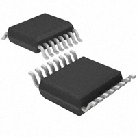
Small 16-Pin TSSOP Package
Temperature Range: –40°C to +85°C
APPLICATIONS
•
•
Energy Exploration Equipment
Seismic Monitoring Systems
The DAC1280 is designed to match the system
components (power supply, clock and reference
voltage) of the companion ADCs, the ADS1281 and
ADS1282. The input to the DAC1280 is a 1s density
modulated bitstream. The DAC1280 output is a
differential current intended for use with an active I/V
converter. The I/V converter provides a voltage output
suitable for performance testing of sensors and
ADCs.
Three gain control pins set the output range in 6dB
steps from 0dB to –36db (±2.5V to ±0.039V
differential). The attenuation ranges match the gains
of the ADS1282 for testing at all gains. The DAC
uses a reference voltage and bias resistor to set the
full-scale output. The resistor can be adjusted to
fine-trim the DAC full-scale.
The SYNC pin aligns the input data sampling to the
CLK phase. A power-down pin shuts down the device
when not in use. The DAC1280 is available in a
small, 16-pin TSSOP package and is fully specified
for operation over –40°C to +85°C temperature range
with a maximum operating temperature of +125°C.
DVDD
VREF
AVDD
External I/V Converter
PWDN
SYNC
CLK
Bitstream
Source
Synchronization
DAC1280
DGND
Current Output
Differential DAC
VOUT
3
GAIN[2:0]
AVSS
1
2
Please be aware that an important notice concerning availability, standard warranty, and use in critical applications of Texas
Instruments semiconductor products and disclaimers thereto appears at the end of this data sheet.
All trademarks are the property of their respective owners.
PRODUCTION DATA information is current as of publication date.
Products conform to specifications per the terms of the Texas
Instruments standard warranty. Production processing does not
necessarily include testing of all parameters.
Copyright © 2010, Texas Instruments Incorporated
�DAC1280
SBAS432A – APRIL 2010 – REVISED SEPTEMBER 2010
www.ti.com
This integrated circuit can be damaged by ESD. Texas Instruments recommends that all integrated circuits be handled with
appropriate precautions. Failure to observe proper handling and installation procedures can cause damage.
ESD damage can range from subtle performance degradation to complete device failure. Precision integrated circuits may be more
susceptible to damage because very small parametric changes could cause the device not to meet its published specifications.
ORDERING INFORMATION
For the most current package and ordering information see the Package Option Addendum at the end of this
document, or see the device product folder at www.ti.com.
ABSOLUTE MAXIMUM RATINGS (1)
Over operating free-air temperature range, unless otherwise noted.
DAC1280
MIN
MAX
UNIT
AVDD to AVSS
–0.3
+5.5
V
AVSS to DGND
–2.8
+0.3
V
DVDD to DGND
–0.3
+3.6
V
Input current, momentary
–100
+100
mA
Input current, continuous
–10
+10
mA
AVSS – 0.3
AVDD + 0.3
V
–0.3
DVDD + 0.3
V
+150
°C
Analog input or output voltage to DGND
Digital input voltage to DGND
Maximum junction temperature
Operating temperature range
–40
+125
°C
Storage temperature range
–60
+150
°C
(1)
Stresses above these ratings may cause permanent damage. Exposure to absolute maximum conditions for extended periods may
degrade device reliability. These are stress ratings only, and functional operation of the device at these or any other conditions beyond
those specified is not implied.
THERMAL INFORMATION
DAC1280
THERMAL METRIC (1)
TSSOP
UNITS
16 PINS
qJA
Junction-to-ambient thermal resistance (2)
111.9
qJCtop
Junction-to-case (top) thermal resistance (3)
33.3
(4)
qJB
Junction-to-board thermal resistance
yJT
Junction-to-top characterization parameter (5)
yJB
Junction-to-board characterization parameter (6)
qJCbot
(1)
(2)
(3)
(4)
(5)
(6)
(7)
2
Junction-to-case (bottom) thermal resistance
52.4
2.0
(7)
°C/W
51.2
—
For more information about traditional and new thermal metrics, see the IC Package Thermal Metrics application report, SPRA953.
The junction-to-ambient thermal resistance under natural convection is obtained in a simulation on a JEDEC-standard, high-K board, as
specified in JESD51-7, in an environment described in JESD51-2a.
The junction-to-case (top) thermal resistance is obtained by simulating a cold plate test on the package top. No specific
JEDEC-standard test exists, but a close description can be found in the ANSI SEMI standard G30-88.
The junction-to-board thermal resistance is obtained by simulating in an environment with a ring cold plate fixture to control the PCB
temperature, as described in JESD51-8.
The junction-to-top characterization parameter, yJT, estimates the junction temperature of a device in a real system and is extracted
from the simulation data for obtaining qJA, using a procedure described in JESD51-2a (sections 6 and 7).
The junction-to-board characterization parameter, yJB, estimates the junction temperature of a device in a real system and is extracted
from the simulation data for obtaining qJA , using a procedure described in JESD51-2a (sections 6 and 7).
The junction-to-case (bottom) thermal resistance is obtained by simulating a cold plate test on the exposed (power) pad. No specific
JEDEC standard test exists, but a close description can be found in the ANSI SEMI standard G30-88.
Submit Documentation Feedback
Copyright © 2010, Texas Instruments Incorporated
Product Folder Link(s): DAC1280
�DAC1280
www.ti.com
SBAS432A – APRIL 2010 – REVISED SEPTEMBER 2010
ELECTRICAL CHARACTERISTICS
Minimum/maximum specifications at –40°C to +85°C, typical specifications at +25°C, AVDD = +2.5V, AVSS = –2.5V, DVDD =
3.3V, CLK = 4.096MHz, VREF = 5V, and RREF = 30kΩ, unless otherwise noted. Refer to circuit configuration shown in
Figure 35.
DAC1280
PARAMETER
TEST CONDITIONS
MIN
TYP
MAX
UNIT
ANALOG OUTPUTS
Full-scale output current
Output common-mode voltage
IFS = (IOUTP – IOUTN) (1)
±1250 ● Gain
Gain = 1/1 to 1/64
(2)
– 0.15
mA
0
+ 0.15
V
Gain = 1/1
±0.02
±0.25
%
Relative to Gain = 1/1
±0.1
±0.5
DC PERFORMANCE (3)
Gain error
Gain match
Gain drift (4)
4
Offset
Gain = 1/1 to 1/64
±50
Offset drift (4)
DC noise (5)
%
ppm/°C
±800
ppm of FS
0.2
ppm of FS/°C
Gain = 1/1
1.2
mVRMS
Gain = 1/2
1.4
mVRMS
Gain = 1/4
1.8
mVRMS
Gain = 1/8
2.9
mVRMS
Gain = 1/16
5.5
mVRMS
Gain = 1/32
10
mVRMS
Gain = 1/64
19
mVRMS
AC PERFORMANCE
Total harmonic
distortion (6)
Gain = 1/1
–125
Gain = 1/2, 1/4, 1/8
–125
dB
Gain = 1/16
–124
dB
Gain = 1/32
–118
dB
Gain = 1/64
–113
dB
120
dB
Gain = 1/2
119
dB
Gain = 1/4
117
dB
Gain = 1/8
114
dB
Gain = 1/16
109
dB
Gain = 1/32
105
dB
Gain = 1/64
99
dB
AVDD, AVSS
60Hz ac, gain = 1/8
85
dB
DVDD
60Hz ac
115
dB
8.2
kHz
THD
Gain = 1/1
Signal-to-noise ratio (7)
SNR
Power-supply rejection
PSR
116
–3dB bandwidth
–118
dB
REFERENCE VOLTAGE INPUT (VREF)
Reference voltage
VREF = VREF – AVSS
Input impedance
(1)
(3)
(4)
(5)
(6)
(7)
5
AVDD + 0.25
V
220
kΩ
Power-down
10
MΩ
TDATA modulated 75% and 25% yielding positive full-scale output and negative full-scale output, respectively. Full-scale positive and
negative output current is given by:
IFS = IOUTP - IOUTN = ±7.5 ·
(2)
2.4
Operating
VREF
· Gain; VREF = 5V, RREF = 30kW nominal
RREF
Gain can be trimmed by adjusting VREF/RREF ratio over the range of 40% to 105% of nominal.
Output common-mode voltage is regulated by the external I/V converter. The specified output common-mode voltage range is: (AVDD +
AVSS)/2 ±0.15V.
Excludes the tolerances of external components.
Drift is calculated over the specified temperature range using the box calculation method.
DC noise measured by ADS1282 with complementing gain over 413Hz bandwidth with DAC output = 0V.
THD = Total harmonic distortion; measured by ADS1282 with complementing gain including first nine harmonics, DAC output =
–0.5dBFS, 31.25Hz.
SNR = Signal-to-noise ratio; measured by ADS1282 with complementing gain over 413Hz bandwidth, DAC output = –0.5dBFS,
31.25Hz.
Submit Documentation Feedback
Copyright © 2010, Texas Instruments Incorporated
Product Folder Link(s): DAC1280
3
�DAC1280
SBAS432A – APRIL 2010 – REVISED SEPTEMBER 2010
www.ti.com
ELECTRICAL CHARACTERISTICS (continued)
Minimum/maximum specifications at –40°C to +85°C, typical specifications at +25°C, AVDD = +2.5V, AVSS = –2.5V, DVDD =
3.3V, CLK = 4.096MHz, VREF = 5V, and RREF = 30kΩ, unless otherwise noted. Refer to circuit configuration shown in
Figure 35.
DAC1280
PARAMETER
TEST CONDITIONS
MIN
TYP
MAX
UNIT
28
30
60
kΩ
REFERENCE RESISTOR (RREF)
Reference resistor
DIGITAL INPUTS (DVDD = 1.65V to 3.6V)
VIH
0.8 × DVDD
DVDD
V
VIL
DGND
0.2 × DVDD
V
–10
10
mA
1
4.096
MHz
Input hysteresis
0.5
Input leakage
0 < VIN < DVDD
V
CLOCK INPUT (fCLK)
Frequency
TDATA INPUT
Frequency
fCLK/16
1s density modulation
25
MHz
75
%
POWER SUPPLY
AVSS
–2.6
0
V
AVDD
AVSS + 4.75
AVSS + 5.25
V
DVDD
1.65
3.6
V
3.7
| mA |
Gain = 1/1
AVDD, AVSS current (8)
DVDD current
Power dissipation
3.6
Power-down
1
10
| mA |
Operating
60
150
mA
Power-down (9)
1
10
Gain = 1/1
18
mW
Power-down
8
mW
mA
TEMPERATURE RANGE
Specified temperature range
–40
+85
°C
Operating temperature range
–40
+125
°C
Storage temperature range
–40
+150
°C
(8)
Typical analog supply current depends on gain, VREF, and RREF:
IAVDD, |IAVSS| = 0.94 ·
(9)
4
VREF
(1 + 22 · Gain)
RREF
CLK and TDATA stopped. Digital inputs maintained at VIH or VIL levels.
Submit Documentation Feedback
Copyright © 2010, Texas Instruments Incorporated
Product Folder Link(s): DAC1280
�DAC1280
www.ti.com
SBAS432A – APRIL 2010 – REVISED SEPTEMBER 2010
TIMING CHARACTERISTICS
space
tCLK
tTDATA
tTCSU
tCPW
1
CLK
2
3
4
5
6
7
8
21
9
Next TDATA
Sample
TDATA
Sample
tCPW
TDATA
tSCSU
tCTHD
SYNC
tSTDAT
tSYLW
DAC OUTPUT
tTSOP
Output
Hold
Output
Update
Figure 1.
TIMING REQUIREMENTS
At TA = –40°C to +85°C and DVDD = 1.65V to 3.6V.
PARAMETER
MIN
TYP
MAX
UNIT
1000
ns
tCLK
CLK period (1/fCLK)
240
tCPW
CLK high or low pulse width
100
ns
tSCSU
SYNC rising edge to CLK rising edge setup time
30
ns
tTCSU
TDATA to CLK rising edge setup time
30
ns
tCTHD
CLK rising edge to TDATA hold time
10
ns
tSYLW
SYNC low pulse width
2
tCLK
tSTDAT
Rising CLK after SYNC high to TDATA sample time
5
tCLK
tTSOP
TDATA sample to output update
4
tCLK
tTDATA
TDATA period
16
tCLK
Submit Documentation Feedback
Copyright © 2010, Texas Instruments Incorporated
Product Folder Link(s): DAC1280
5
�DAC1280
SBAS432A – APRIL 2010 – REVISED SEPTEMBER 2010
www.ti.com
DEVICE INFORMATION
PW PACKAGE
TSSOP-16
(TOP VIEW)
CLK
1
16
PWDN
TDATA
2
15
IOUTP
SYNC
3
14
IOUTN
DGND
4
13
NC
DAC1280
DVDD
5
12
AVDD
GAIN0
6
11
AVSS
GAIN1
7
10
RREF
GAIN2
8
9
VREF
TERMINAL FUNCTIONS
TERMINAL
6
NAME
NO.
I/O
CLK
1
Digital Input
4.096MHz master clock
DESCRIPTION
TDATA
2
Digital Input
Bitstream digital data
Synchronize control
SYNC
3
Digital Input
DGND
4
Digital Ground
Digital ground
DVDD
5
Digital Supply
Digital power supply
GAIN0
6
Digital Input
Gain select 0
GAIN1
7
Digital Input
Gain select 1
GAIN2
8
Digital Input
Gain select 2
VREF
9
Analog Input
Voltage reference input
RREF
10
Analog
Full-scale range resistor
AVSS
11
Analog Supply
Negative analog power supply, VREF common, RREF common
AVDD
12
Analog Supply
Positive analog power supply
NC
13
—
IOUTN
14
Analog Output
No connection; do not connect externally.
Negative signal output current
IOUTP
15
Analog Output
Positive signal output current
PWDN
16
Digital Input
Power-down control; active low
Submit Documentation Feedback
Copyright © 2010, Texas Instruments Incorporated
Product Folder Link(s): DAC1280
�DAC1280
www.ti.com
SBAS432A – APRIL 2010 – REVISED SEPTEMBER 2010
TYPICAL CHARACTERISTICS
At TA = +25°C, AVDD = +2.5V, AVSS = +2.5V, DVDD = +3.3V, CLK = 4.096MHz, VREF = +5V, and RREF = 30kΩ, unless
otherwise noted. Data acquired using circuit configuration shown in Figure 35. THD and SNR measured by ADS1282 (1ms
sampling and complement gain setting).
OUTPUT SPECTRUM
OUTPUT SPECTRUM
0
0
Amplitude (dB)
-40
-60
-80
-100
-120
-140
Gain = 1/2
4k FFT
VOUT = -0.5dBFS, 31.25Hz
THD = -128.9dB
SNR = 119.5dB
-20
-40
Amplitude (dB)
Gain = 1/1
4k FFT
VOUT = -0.5dBFS, 31.25Hz
THD = -129.2dB
SNR = 120.5dB
-20
-60
-80
-100
-120
-140
-160
-160
-180
-180
-200
-200
0
50
100 150 200 250 300 350
400 450 500
0
50
Frequency (Hz)
Figure 3.
OUTPUT SPECTRUM
OUTPUT SPECTRUM
0
0
-40
-60
-80
-100
-120
-140
Gain = 1/8
4k FFT
VOUT = -0.5dBFS, 31.25Hz
THD = -126dB
SNR = 114.1dB
-20
-40
Amplitude (dB)
Gain = 1/4
4k FFT
VOUT = -0.5dBFS, 31.25Hz
THD = -127.6dB
SNR = 117.4dB
-20
Amplitude (dB)
400 450 500
Frequency (Hz)
Figure 2.
-60
-80
-100
-120
-140
-160
-160
-180
-180
-200
-200
0
50
100 150 200 250 300 350
400 450 500
0
50
Frequency (Hz)
100 150 200 250 300 350
400 450 500
Frequency (Hz)
Figure 4.
Figure 5.
OUTPUT SPECTRUM
OUTPUT SPECTRUM
0
0
-40
-60
-80
-100
-120
-140
-40
-60
-80
-100
-120
-140
-160
-160
-180
-180
-200
Gain = 1/32
8k FFT
VOUT = -0.5dBFS, 31.25Hz
THD = -117.6dB
SNR = 104.8dB
-20
Amplitude (dB)
Gain = 1/16
8k FFT
VOUT = -0.5dBFS, 31.25Hz
THD = -124.8dB
SNR = 109.4dB
-20
Amplitude (dB)
100 150 200 250 300 350
-200
0
50
100 150 200 250 300 350
400 450 500
0
Frequency (Hz)
50
100 150 200 250 300 350
400 450 500
Frequency (Hz)
Figure 6.
Figure 7.
Submit Documentation Feedback
Copyright © 2010, Texas Instruments Incorporated
Product Folder Link(s): DAC1280
7
�DAC1280
SBAS432A – APRIL 2010 – REVISED SEPTEMBER 2010
www.ti.com
TYPICAL CHARACTERISTICS (continued)
At TA = +25°C, AVDD = +2.5V, AVSS = +2.5V, DVDD = +3.3V, CLK = 4.096MHz, VREF = +5V, and RREF = 30kΩ, unless
otherwise noted. Data acquired using circuit configuration shown in Figure 35. THD and SNR measured by ADS1282 (1ms
sampling and complement gain setting).
OUTPUT SPECTRUM
GAIN MATCH HISTOGRAM
0
10
Amplitude (dB)
-40
-60
-80
-100
-120
30 Units
Gain Match over TA = -40°C to +85°C
8
Occurrences
Gain = 1/64
8k FFT
VOUT = -0.5dBFS, 31.25Hz
THD = -113.1dB
SNR = 99.3dB
-20
6
4
-140
2
-160
-180
0
0
50
100 150 200 250 300 350
0
200
400
600
800
1000
1200
1400
1600
1800
2000
2200
2400
2600
2800
3000
3200
3400
3600
3800
4000
-200
400 450 500
Frequency (Hz)
Absolute Gain Match (ppm)
Figure 8.
Figure 9.
GAIN ERROR vs TEMPERATURE
GAIN ERROR HISTOGRAM
1500
10
G = 1/1
G = 1/2
G = 1/4
G = 1/8
G = 1/16
G = 1/32
G = 1/64
30 Units
Gain = 1/1
8
500
Occurrences
Gain Error (ppm)
1000
0
-500
6
4
2
-1000
0
-55
-35
-15
5
45
25
65
85
105
-1000
-900
-800
-700
-600
-500
-400
-300
-200
-100
0
100
200
300
400
500
600
700
800
900
1000
-1500
125
Temperature (°C)
Gain Error (ppm)
Figure 10.
Figure 11.
OFFSET vs TEMPERATURE
OFFSET HISTOGRAM
10
200
G = 1/1
G = 1/2
G = 1/4
G = 1/8
150
30 Units
Gain = 1/1
8
Occurrences
Offset (ppm, FS)
100
G = 1/16
G = 1/32
G = 1/64
50
0
-50
-100
6
4
2
-150
-55
-35
-15
5
25
45
Temperature (°C)
65
85
105
125
-250
-225
-200
-175
-150
-125
-100
-75
-50
-25
0
25
50
75
100
125
150
175
200
225
250
0
-200
Offset (ppm, FS)
Figure 12.
8
Figure 13.
Submit Documentation Feedback
Copyright © 2010, Texas Instruments Incorporated
Product Folder Link(s): DAC1280
�DAC1280
www.ti.com
SBAS432A – APRIL 2010 – REVISED SEPTEMBER 2010
TYPICAL CHARACTERISTICS (continued)
At TA = +25°C, AVDD = +2.5V, AVSS = +2.5V, DVDD = +3.3V, CLK = 4.096MHz, VREF = +5V, and RREF = 30kΩ, unless
otherwise noted. Data acquired using circuit configuration shown in Figure 35. THD and SNR measured by ADS1282 (1ms
sampling and complement gain setting).
THD vs TEMPERATURE
G = 1/1
G = 1/2
G = 1/4
G = 1/8
-105
-110
G = 1/16
G = 1/32
G = 1/64
G = 1/1
Signal-to-Noise Ratio (dB)
Total Harmonic Distortion (dB)
SNR vs TEMPERATURE
125
-100
-115
-120
-125
-130
G = 1/4
115
G = 1/8
110
G = 1/16
G = 1/32
105
100
G = 1/64
95
-135
-55
-35
-15
5
45
25
65
85
105
125
-55
-35
-15
Figure 14.
THD vs OUTPUT FREQUENCY
85
105
125
SNR vs OUTPUT FREQUENCY
G = 1/1
G = 1/2
G = 1/4
G = 1/8
G = 1/16
G = 1/32
G = 1/64
G = 1/1
Signal-to-Noise Ratio (dB)
Total Harmonic Distortion (dB)
65
125
-105
-110
-115
-120
-125
-130
120
G = 1/4
G = 1/2
115
G = 1/8
G = 1/16
110
105
G = 1/32
100
0.1
1
10
100
0.1
1k
1
Output Frequency (Hz)
10
100
1k
Output Frequency (Hz)
Figure 16.
Figure 17.
THD vs OUTPUT AMPLITUDE(1)
SNR vs OUTPUT AMPLITUDE
-20
125
Signal-to-Noise Ratio (dB)
-40
-60
-80
-120
45
25
Figure 15.
-100
-100
5
Temperature (°C)
Temperature (°C)
Total Harmonic Distortion (dB)
G = 1/2
120
G = 1/1
G = 1/2
G = 1/4
G = 1/8
G = 1/16
G = 1/32
G = 1/64
-140
-100 -90 -80 -70 -60
-50 -40 -30
-20 -10
0
100
G = 1/1
G = 1/2
G = 1/4
G = 1/8
G = 1/16
G = 1/32
G = 1/64
75
50
25
0
-100
Output Amplitude (dB)
-80
-60
-40
-20
0
Output Amplitude (dB)
(1) THD measurement noise limited for amplitudes less than –10dB.
Figure 18.
Figure 19.
Submit Documentation Feedback
Copyright © 2010, Texas Instruments Incorporated
Product Folder Link(s): DAC1280
9
�DAC1280
SBAS432A – APRIL 2010 – REVISED SEPTEMBER 2010
www.ti.com
TYPICAL CHARACTERISTICS (continued)
At TA = +25°C, AVDD = +2.5V, AVSS = +2.5V, DVDD = +3.3V, CLK = 4.096MHz, VREF = +5V, and RREF = 30kΩ, unless
otherwise noted. Data acquired using circuit configuration shown in Figure 35. THD and SNR measured by ADS1282 (1ms
sampling and complement gain setting).
THD vs CLK
SNR vs CLK
125
G = 1/1
G = 1/2
G = 1/4
G = 1/8
-95
-100
G (MHz)
= 1/16
CLK
G = 1/32
G = 1/64
THD resolution of low
gains limited by FFT size
-105
-110
-115
-120
-125
-130
fO = CLK/2 , -0.5dBFS
2.0
2.5
3.0
3.5
110
105
100
G = 1/1
G = 1/2
G = 1/4
G = 1/8
4.5
4.0
G = 1/16
G = 1/32
G = 1/64
90
-135
1.5
115
95
17
1.0
17
fO = CLK/2 , -0.5dBFS
120
Signal-to-Noise Ratio (dB)
Total Harmonic Distortion (dB)
-90
1.0
1.5
2.0
2.5
CLK (MHz)
Figure 20.
THD vs VREF
SNR vs VREF
G = 1/1
G = 1/2
G = 1/4
-100
-105
G = 1/8
G = 1/16
G = 1/32
G = 1/64
120
Signal-to-Noise Ratio (dB)
Total Harmonic Distortion (dB)
4.5
4.0
125
-110
-115
-120
-125
-130
115
110
105
100
95
G = 1/8
G = 1/16
G = 1/32
G = 1/64
G = 1/1
G = 1/2
G = 1/4
90
-135
85
2.5
3.0
3.5
4.0
4.5
5.0
5.2
2.5
3.0
3.5
Reference Voltage (V)
4.5
4.0
5.0
Figure 23.
THD HISTOGRAM
ANALOG POWER-SUPPLY CURRENT vs
TEMPERATURE
G = 1/1
G = 1/4
G = 1/16
G = 1/64
10
5
0
4
AVDD Current (mA)
30 Units
5.2
Reference Voltage (V)
Figure 22.
15
Occurrences
3.5
Figure 21.
-95
20
3.0
CLK (MHz)
G = 1/1
G = 1/2
G = 1/4
G = 1/8
3
G = 1/16
G = 1/32
G = 1/64
2
1
-136
-134
-132
-130
-128
-126
-124
-122
-120
-118
-116
-114
-112
-110
-108
-106
-104
-102
-100
0
-55
-35
-15
5
25
45
65
85
105
125
Temperature (°C)
Total Harmonic Distortion (dB)
Figure 24.
10
Figure 25.
Submit Documentation Feedback
Copyright © 2010, Texas Instruments Incorporated
Product Folder Link(s): DAC1280
�DAC1280
www.ti.com
SBAS432A – APRIL 2010 – REVISED SEPTEMBER 2010
DAC1280 OVERVIEW
The DAC1280 is a high-accuracy digital-to-analog
converter (DAC) that provides outstanding THD
performance together with low noise. The DAC1280
is suitable for the demanding requirements of energy
exploration and precision instrumentation where a
low-distortion test signal is needed.
Figure 26 shows the DAC1280 block diagram. The
DAC provides a signal output proportional to a 1s
density input. The DAC design is a multi-tap,
current-steering filter that provides a differential
current output. An external current-to-voltage (I-V)
converter is required to provide a voltage output. VREF
and RREF program the full-scale current, and
GAIN[2:0] pins set the output range.
The current-steering stage switches the tap current to
either output, IOUTP or IOUTN, as a result of the
sampling of TDATA. A higher 1s density directs more
current toward IOUTP and less to IOUTN.
Conversely, a higher density of 0s directs more
current to IOUTN than to IOUTP. Steering of the
output current yields an average output proportional
to the 1s density input.
An integrated power-on-reset (POR) function resets
the current taps, resulting in a zero differential output
signal at power-up. The active low PWDN input
powers down the device to a low-power (mW) state.
The SYNC input synchronizes the DAC1280 TDATA
sampling.
VREF and RREF establish an internal current that is
mirrored to a multi-tap, current-steering filter stage
through a reference current control block. The output
of the control block is set by the GAIN[2:0] inputs,
which fix the weighted tap currents in one of seven
ranges. The magnitude of the tap currents results in
the maximum differential output current ranges of
1250mA to the lowest range of 19.5mA.
AVDD
DVDD
POR
Current Taps
PWDN
Reference
Current
Control
GAIN2
GAIN1
GAIN0
IOUTP
IOUTN
VREF
Divider
RREF
SYNC
TDATA
CLK
Reset
Reset
D
Tap Control
Reset
Common-Mode
Current
D
CLK/16
4-bit
Counter
DAC1280
DGND
AVSS
Figure 26. DAC1280 Block Diagram
Submit Documentation Feedback
Copyright © 2010, Texas Instruments Incorporated
Product Folder Link(s): DAC1280
11
�DAC1280
SBAS432A – APRIL 2010 – REVISED SEPTEMBER 2010
www.ti.com
DAC1280 Basics
Output Scaling
The basic requirements of DAC1280 operation are a
clock, a bitstream input, an external current-to-voltage
converter, and a reference voltage. The bitstream
originates either from an FPGA-based digital
modulator or playback from a ROM device holding a
stored bitstream file. The external reference voltage is
+5V and should be precision (low drift and low noise).
The current-to-voltage converter is an active circuit.
The amplifiers used for the current-to-voltage
converter should have good dynamic characteristics
(low THD) with low noise. Figure 27 illustrates the
system block diagram.
The full-scale output of the DAC1280 is set by the
reference voltage and an external reference resistor.
The GAIN[2:0] control pins select one of seven output
ranges. In operation, the reference voltage and
reference resistor are usually fixed, and the DAC
output range is selected by the gain pins.
5V
Reference
Clock
4.096MHz
CLK
VREF
IOUTP
Bitstream
Source
TDATA
DAC1280
256kHz
VCOM
VN
(1)
Voltage
Output
I/V
The DAC1280 differential
determined by Equation 1:
Differential Output Current = 7.5 ·
output
current
is
VREF
(TDATA - 50%)
· Gain ·
25%
RREF
Where:
•
•
•
•
VREF = 5V (nominal)
RREF = 30kΩ (nominal)
Gain = 1/1 to 1/64
TDATA = TDATA 1s density, ranging 25% to
75%
(1)
VP
IOUTN
The DAC full-scale output can be fine-trimmed, if
VREF
(1)
VCOM = midsupply voltage.
Figure 27. DAC1280 System Block Diagram
Output Voltage
As shown in the system block diagram, the external
I/V circuit converts the current output of the DAC to a
voltage output. The voltage output of the I/V circuit is
differential, as shown in Figure 28. The
common-mode output voltage (VCOM) at the I/V circuit
is normally set to the midsupply point of the DAC.
The differential output voltage is ±2.5V/gain.
VN
desired, by changing the RREF ratio from the nominal
values of VREF = 5V and RREF = 30kΩ. See the
Electrical Characteristics for the adjustment range.
The external current-to-voltage converter scales the
DAC output current into an output voltage. Table 1
shows the DAC1280 gain (differential output current
to bitstream density) and the resulting output voltage
of the external current-to-voltage converter.
VCOM + 1.25V · Gain
VCOM
VCOM - 1.25V · Gain
VCOM + 1.25V · Gain
I/V
VP
VCOM
VCOM - 1.25V · Gain
Differential output voltage = VP - VN = ±2.5V · Gain
VCOM = 0V (dual analog supply), +2.5V (single +5V analog supply)
Figure 28. I/V Converter Output Voltage
12
Submit Documentation Feedback
Copyright © 2010, Texas Instruments Incorporated
Product Folder Link(s): DAC1280
�DAC1280
www.ti.com
SBAS432A – APRIL 2010 – REVISED SEPTEMBER 2010
Table 1. DAC1280 Ideal Output Scaling (1)
(1)
TDATA 1s DENSITY (%)
IOUTP – IOUTN (mA)
VP – VN (V)
25
–1250 ● Gain
–2.5 ● Gain
37.5
–625 ● Gain
–1.25 ● Gain
50
0
0
62.5
+625 ● Gain
+1.25 ● Gain
75
+1250 ● Gain
+2.5 ● Gain
VREF = 5V, RREF = 30kΩ, external current-to-voltage converter resistors = 2kΩ. Output current and
voltage are differential. Excludes the effects of DAC1280 offset, gain and linearity errors, errors in
reference voltage, errors as a result of external resistors, and errors from the external
current-to-voltage conversion. Refer to Figure 27.
VREF Reference Voltage Input
RREF Reference Resistor
The DAC1280 requires an external reference for
operation. The reference voltage of the DAC1280 is
defined as the voltage difference between VREF and
AVSS (that is, VREF = VREF – AVSS). The DAC1280
output directly scales with VREF; consequently, noise
or drift on the reference appear at the DAC1280
output. A low-drift and low-noise precision reference
is recommended for best performance.
A 30kΩ resistor, connected from VREF to AVSS, is
required for operation. This resistor, in combination
with VREF, is used to set the DAC full-scale output.
The resistor can be used to fine-trim the DAC gain by
changing the value from the nominal 30kΩ. See the
Output Scaling section for more information.
The external resistor accuracy and temperature drift
directly affect the DAC1280 output accuracy. A
low-drift, precision resistor is recommended for best
performance. Connect the resistor directly to the
RREF and AVSS pins using short and direct traces.
Keep RREF stray capacitance to a minimum. Refer to
Figure 29 for the reference input connection.
For best layout, connect the ground pin of the
external reference directly to the AVSS terminal to
minimize possible crosstalk. A recommended 0.1mF
ceramic capacitor connected directly across VREF
and AVSS reduces noise susceptibility.
Figure 29 shows the reference input voltage and
reference resistor connection to the DAC1280. The
DAC1280 loads VREF with 220kΩ. The 220kΩ
resistor disconnects in power-down mode.
+V
VREF
+5V
Reference
117kW
103kW
(1)
0.1mF
Power-down
Switch
AVSS
-2.5V
RREF
30kW
(1)
Current
used to
set Full-Scale
RREF
Recommended noise capacitor.
Figure 29. Reference Input Connection
Submit Documentation Feedback
Copyright © 2010, Texas Instruments Incorporated
Product Folder Link(s): DAC1280
13
�DAC1280
SBAS432A – APRIL 2010 – REVISED SEPTEMBER 2010
www.ti.com
Pin Descriptions
GAIN[2:0] Pins
The DAC1280 output range can be set in 6dB steps,
controlled by three digital inputs. The ranges match
the gains of the ADS1282 for testing at all gains.
Table 2 shows the output range versus gain settings
for the DAC1280.
TDATA bits are '1'), the differential output current is at
a positive maximum value; when the 1s density input
is at 25% (on average, three out of four TDATA bits
are '0'), the differential output current is at a negative
maximum value. When the 1s density is 50% (on
average, an equal number of '1's and '0's), the
differential output current is 0. See Table 1.
NOTE: It is recommended that the DAC and ADC
use complementary gains when testing. ADC
instability may result because of the combination of
the noise-shaped DAC input and if the ratio of
ADC/DAC gain is greater than 2.
TDATA is sampled by the DAC1280 at CLK/16 rate
(nominally 256kHz with 4.096MHz master clock), and
therefore, the sampling of TDATA can have 16 CLK
cycles of uncertainty. SYNC can be used to eliminate
the uncertainty by synchronizing TDATA sampling.
Synchronizing TDATA sampling yields a consistent
test signal phase response.
IOUTP, IOUTN
SYNC
IOUTP and IOUTN are the differential current
outputs. The outputs are intended to be used in
conjunction with an external current-to-voltage
converter, as shown in the circuit of Figure 35. Note
that the current-to-voltage converter also sets the
DAC1280 DAC output common-mode voltage. See
specifications for the allowable common-mode output
voltage.
SYNC is an input used to synchronize the CLK cycle
at which the DAC1280 samples TDATA. When SYNC
is low, the internal CLK is disabled (ignoring TDATA
input), and the DAC output is held constant. When
SYNC is taken high, the DAC resumes sampling
TDATA on the sixth rising CLK edge after SYNC is
high. TDATA is then sampled on periodic 16 CLK
intervals. Four CLK cycles propagate from the
TDATA sample to the physical update of the DAC
output. If SYNC is not used, tie SYNC high. Refer to
Figure 1 for an illustration of the SYNC timing
sequence.
CLK
CLK is the master clock input to the DAC1280
(nominally 4.096MHz). As with any high-performance
ADC or DAC, a high-quality, low-jitter clock source is
essential. A crystal oscillator clock source is
recommended. Make sure to avoid excess ringing on
the clock input: keeping the printed circuit board
(PCB) trace short, and using source termination
resistors (20Ω to 50Ω) placed close to the source
end, often helps.
TDATA
TDATA is the digital signal input and determines the
output frequency and amplitude. TDATA is encoded
as a 1s density bitstream where the DAC1280 output
is proportional to the 1s density. When the 1s density
input is 75% (that is, on average, three out of four
PWDN
PWDN is an input used to power down the DAC1280.
To power down the device, take the PWDN pin low.
In power-down mode, the device bias is disabled and
the outputs are Hi-Z. Note that the digital inputs must
remain defined in power-down mode either as logic
low or logic high; do not float the inputs. Disable the
CLK and TDATA inputs to minimize power-supply
leakage. To exit power-down mode, take PWDN high.
The DAC1280 output is reset to zero when the
PWDN pin goes high.
Table 2. Differential Current Output vs Gain Setting (1)
(1)
14
GAIN[2:0] PINS
GAIN
GAIN (dB)
IOUTP – IOUTN (mA)
000
1/1
0
±1250
VP – VN (V)
±2.5
001
1/2
–6
±625
±1.25
010
1/4
–12
±312
±0.625
011
1/8
–18
±156
±0.312
100
1/16
–24
±78.1
±0.156
101
1/32
–30
±39.1
±0.0781
110
1/64
–36
±19.5
±0.0391
TDATA 1s density 25%/75%, VREF = 5V, RREF = 30kΩ, external current-to-voltage converter resistors = 2kΩ. Output current and voltage
are differential. Excludes the effects of DAC1280 offset, gain and linearity errors, errors in reference voltage, errors caused by external
resistors, and errors as a result of external current-to-voltage conversion. See Figure 27.
Submit Documentation Feedback
Copyright © 2010, Texas Instruments Incorporated
Product Folder Link(s): DAC1280
�DAC1280
www.ti.com
SBAS432A – APRIL 2010 – REVISED SEPTEMBER 2010
Table 3. DAC1280 Power Consumption
Power Supplies
The DAC1280 has two power supplies, analog and
digital. The analog supply is 5V and can be
configured for bipolar operation (with AVDD = 2.5V
and AVSS = –2.5V), or configured for unipolar
operation (with AVDD = 5V and AVSS grounded).
The common-mode voltage of the external I/V
converter is normally set to the DAC1280 midsupply.
Because AVSS is shared with the reference low
terminal, and the analog supply pins draw
signal-dependent current, the external reference
ground terminal should connect to AVSS using a star
connection close to the DAC. This approach helps to
minimize power-supply coupling to the reference
input.
DVDD is the digital supply and operates over the
range of 1.65V to 3.6V. Bypass the DVDD as well as
the analog supplies with a capacitor (minimum 1mF).
The power supplies can be sequenced in any order.
At power-on, the latter occurrence of DVDD
exceeding 1V, or (AVDD – AVSS) exceeding 3V,
causes an internal power-on reset (POR) to occur. A
POR resets the output to zero. After reset, the first
sampling of TDATA by the DAC1280 occurs on the
sixth CLK rising edge, as Figure 30 shows.
DVDD
1V
AVDD-AVSS
3V
DAC1280 POWER (mW)
1/1
18
1/2
9.6
1/4
5.3
1/8
3.1
1/16
2.1
1/32
1.5
1/64
1.2
Offset and Gain Error
The DAC1280 features low offset error (±50ppmFS,
typical) and low gain error (±0.02%, gain = 1/1,
typical). Gain match is specified as the maximum
error of gain = 1/1 relative to gains 1/2 to 1/64 of a
single device. Typical gain match error is ±0.1%.
Offset and gain drift are also very low for the
DAC1280. Drift is calculated using the box calculation
method:
Max - Min
(ppm/°C)
Drift calculation:
Temp Range
(2)
Where Max and Min are respectively the maximum
and minimum offset or gain errors (in ppm) recorded
over the specified temperature range of –40°C to
+85°C.
Noise Performance (SNR)
Internal POR
TDATA
First TDATA Sample
1
CLK
GAIN
2
3
4
5
6
Figure 30. Power-On Sequence
Power Consumption
The total power consumption is the power consumed
by the DAC1280 plus that of the external
current-to-voltage converter. The power consumption
of the DAC1280, in turn, depends on the gain setting.
Table 3 summarizes the DAC1280 power
consumption.
The DAC1280 achieves excellent signal-to-noise ratio
(SNR) performance. The SNR figures were obtained
using the circuit of Figure 35. SNR is measured by
the ADS1282 over a bandwidth of 0 to 413Hz (with
1ms sampling). The ADC and DAC have
complementing gains for each measurement.
SNR is measured with a signal output of –0.5dBFS
and 31.25Hz, then taking the Fast Fourier
Transformation (FFT) of the ADC data, and
calculating the noise power over the specified
bandwidth. The dc, fundamental, and harmonic bins
are removed for the SNR calculations. Measured this
way, SNR is the combination of the individual noise
sources including ADC noise, DAC1280 noise,
voltage and current noise of the external op amp, and
thermal noise of the I/V resistors.
Submit Documentation Feedback
Copyright © 2010, Texas Instruments Incorporated
Product Folder Link(s): DAC1280
15
�DAC1280
SBAS432A – APRIL 2010 – REVISED SEPTEMBER 2010
www.ti.com
If desired, SNR can be improved by decreasing the
2kΩ I/V feedback resistors and then applying
correspondingly higher DAC1280 gains. Decreasing
the resistor values results in a decrease of the
maximum output amplitude as shown in Figure 31,
SNR versus output amplitude for I/V resistor values of
2kΩ, 1kΩ, and 500Ω. If decreasing the I/V feedback
resistor, increase the I/V capacitor proportionally to
maintain the same low-pass corner frequency.
settling, the I/V filter network is also settling. The
suggested I/V RC components (R = 2kΩ, C = 1nF)
result in an I/V time constant of approximately 2ms.
Figure 32 shows the composite step response of the
circuit in Figure 35.
LARGE-SIGNAL STEP RESPONSE
VOUT
SNR vs OUTPUT AMPLITUDE
125
1V/div
Signal-to-Noise Ratio (dB)
RI/V = 500W
120
115
Input Step
RI/V = 2kW
110
RI/V = 1kW
105
Time (50ms/div)
100
Figure 32. DAC1280 Large-Signal Step Response
(Noise Removed for Clarity)
95
-36
-30
-24
-18
-12
-6
0
Gain (dB)
Frequency Response
Figure 31. SNR vs Output Amplitude
DC Noise
DC noise is measured by the ADS1282 with the
circuit configuration of Figure 35. The measurement
bandwidth is 413Hz and the ADC is set to a
complementing gain. The measurement is taken with
a 50% 1s density input that results in a 0V differential
signal output. DC noise is the standard deviation
(RMS, referred to output).
The DAC1280 low-pass filters the bitstream input,
resulting in a sinc2 frequency response profile with
the first notch (zero) located at fCLK/160 (25.6kHz with
CLK = 4.096MHz). However, the aspect of noise
shaping of the digital modulator may result in rising
noise versus frequency. This rising noise may limit
the usable bandwidth to less than the DAC inherent
bandwidth. Figure 33 illustrates the DAC1280
frequency response.
OUTPUT FREQUENCY RESPONSE
0
Total Harmonic Distortion (THD)
-10
Magnitude (dB)
The DAC1280 achieves excellent THD performance.
THD was characterized using the circuit shown in
Figure 35 and the ADS1282 with complementary
ADC gain settings for each DAC gain. Note that a
low-distortion
op
amp
for
current-to-voltage
conversion (such as the OPA211) is essential in
order to achieve rated performance.
CLK = 4.096MHz
Excludes I/V Filter Rolloff
-20
-30
-40
-50
Settling Time
The settling time of the DAC1280 resulting from a
step input change consists of the DAC1280 settling
time and the I/V filter settling time. Other filter
components used in the DAC signal path may also
add to the settling time.
-60
0
5
10
15
20
25
30
35
40
45
50
Output Frequency (kHz)
Figure 33. Output Frequency Response
When a step input is applied to TDATA, the DAC
output begins to change. The DAC completely settles
in 78ms (CLK = 4.096MHz). As the DAC output is
16
Submit Documentation Feedback
Copyright © 2010, Texas Instruments Incorporated
Product Folder Link(s): DAC1280
�DAC1280
www.ti.com
SBAS432A – APRIL 2010 – REVISED SEPTEMBER 2010
Seismic System
Figure 34 illustrates an example of a three-channel
seismic measurement system that consists of the
DAC1280 and three ADS1282s.
geophone or routed through an external switch
network. The DAC input signal is sourced from a
bitstream pattern stored in the device flash memory
(as shown here), or supplied directly from a bitstream
modulator implemented in an FPGA.
The DAC1280 drives the ADS1282s and the
geophone sensors for testing. The DAC signal can be
routed through the ADS1282 input mux to the
4.096MHz
Clock
TDATA
I/V
Converter
DAC1280
Serial
Flash
Memory
CLK/16
Switch
Network
ADS1282
Geophone
Serial
Bus
mController
or
FPGA
Switch
Network
ADS1282
Geophone
Switch
Network
+5V
Reference
ADS1282
Geophone
Figure 34. Three-Channel Seismic System Block Diagram
Submit Documentation Feedback
Copyright © 2010, Texas Instruments Incorporated
Product Folder Link(s): DAC1280
17
�DAC1280
SBAS432A – APRIL 2010 – REVISED SEPTEMBER 2010
www.ti.com
Basic Connection
reference bias resistor is a 31.6kΩ precision resistor.
Increasing the resistor value (from 30kΩ nominal)
reduces the DAC full-scale output by –0.5db, to avoid
clipping of the ADC. The filter series resistance and
the VREF input impedance interaction results in a
gain error of –0.5%
Figure 35 shows a basic connection of the DAC1280,
with an external op amp current-to-voltage converter.
Bipolar analog supplies are shown (±2.5V).
Single-supply operation (+5V) is also possible by
grounding AVSS; for single-supply operation, bias the
current-to-voltage converter noninverting terminals to
midsupply.
Two OPA211s and RA, RB implement the
current-to-voltage converter. RA and RB scale the
DAC current output to a voltage output. 1nF
capacitors filter the DAC sampling noise, and 50Ω
resistors isolate the op amp from capacitive loads.
Place the current-to-voltage converter circuit
components close to the DAC1280 using a
symmetrical layout. A comparator, such as the
TLV3491, translates the PWDN logic level signal to
the OPA211 level requirements.
A low-noise, low-drift, precision reference is
recommended for operation with the DAC1280, such
as the REF5050. The REF5045 or REF02 are also
suitable, depending on the end system SNR
requirements. The REF5045 operates from a
minimum 5V power supply; the REF5050 operates
from a minimum 5.3V power supply; and the REF02
operates from a minimum 8.5V power supply. The
optional reference RC filter reduces broadband
reference noise. Using the filter network, loading of
the VREF input results in –0.5% gain error. The
+2.8V
(2)
1kW
1mF
REF5050
1mF
(2)
100W
100mF
RA
(2)
(1)
2kW
1nF
-2.5V
C0G/Film
+2.5V
-2.5V
+3.3V
+2.5V
0.1mF
50W
1mF
Controller
1 mF
DVDD
CLK
VREF
VN
OPA211
AVDD
CLK
IOUTP
-2.5V
IOUTN
+2.5V
20W to 50W
TDATA
TDATA
SYNC
SYNC
DAC1280
GAIN[2:0]
PWDN
RREF AVSS
50W
VP
OPA211
(1)
GAIN2
1 mF
31.6kW
GAIN1
-2.5V
-2.5V
1nF
C0G/Film
GAIN0
+3.3V
PWDN
2kW
1MW
+2.5V
1MW
RB
(1)
TLV3491
-2.5V
1MW
(1)
Precision resistors.
(2)
Optional reference noise filter.
Figure 35. Basic Connection
18
Submit Documentation Feedback
Copyright © 2010, Texas Instruments Incorporated
Product Folder Link(s): DAC1280
�PACKAGE OPTION ADDENDUM
www.ti.com
10-Dec-2020
PACKAGING INFORMATION
Orderable Device
Status
(1)
Package Type Package Pins Package
Drawing
Qty
Eco Plan
(2)
Lead finish/
Ball material
MSL Peak Temp
Op Temp (°C)
Device Marking
(3)
(4/5)
(6)
DAC1280IPW
ACTIVE
TSSOP
PW
16
90
RoHS & Green
NIPDAU
Level-1-260C-UNLIM
-40 to 85
DAC1280
DAC1280IPWR
ACTIVE
TSSOP
PW
16
2000
RoHS & Green
NIPDAU
Level-1-260C-UNLIM
-40 to 85
DAC1280
(1)
The marketing status values are defined as follows:
ACTIVE: Product device recommended for new designs.
LIFEBUY: TI has announced that the device will be discontinued, and a lifetime-buy period is in effect.
NRND: Not recommended for new designs. Device is in production to support existing customers, but TI does not recommend using this part in a new design.
PREVIEW: Device has been announced but is not in production. Samples may or may not be available.
OBSOLETE: TI has discontinued the production of the device.
(2)
RoHS: TI defines "RoHS" to mean semiconductor products that are compliant with the current EU RoHS requirements for all 10 RoHS substances, including the requirement that RoHS substance
do not exceed 0.1% by weight in homogeneous materials. Where designed to be soldered at high temperatures, "RoHS" products are suitable for use in specified lead-free processes. TI may
reference these types of products as "Pb-Free".
RoHS Exempt: TI defines "RoHS Exempt" to mean products that contain lead but are compliant with EU RoHS pursuant to a specific EU RoHS exemption.
Green: TI defines "Green" to mean the content of Chlorine (Cl) and Bromine (Br) based flame retardants meet JS709B low halogen requirements of