®
DAC2814
DUAL 12-BIT DIGITAL-TO-ANALOG
CONVERTER (Serial Interface)
FEATURES
● COMPLETE DUAL DAC —
INCLUDES INTERNAL REFERENCES AND
OUTPUT AMPLIFIERS
● GUARANTEED SPECIFICATIONS OVER
TEMPERATURE
● GUARANTEED MONOTONIC OVER
TEMPERATURE
● HIGH-SPEED SERIAL INTERFACE
(10MHz CLOCK)
● LOW POWER: 300mW (150mW/DAC)
● LOW GAIN DRIFT: 5ppm/°C
● LOW NONLINEARITY: ±1/2 LSB max
● UNIPOLAR OR BIPOLAR OUTPUT
● CLEAR/RESET TO UNIPOLAR OR
BIPOLAR ZERO
DESCRIPTION
DAC2814
The DAC2814 is one in a family of dual and quad 12bit digital-to-analog converters. Serial, 8-bit, 12-bit
interfaces are available.
The DAC2814 is complete. It contains CMOS logic,
switches, a high-performance buried-zener reference,
and low-noise bipolar output amplifiers. No external
components are required for either unipolar 0 to 10V,
0 to –10V, or bipolar ±10V output ranges.
The DAC2814 has a high-speed serial interface
capable of being clocked at 10MHz. Serial data are
clocked DAC B MSB first into a 24-bit shift register,
then strobed into each DAC separately or simultaneously as required. The DAC has an asynchronous
clear control for reset to unipolar or bipolar zero
depending on the mode selected. This feature is useful
for power-on reset or system calibration. The DAC2814
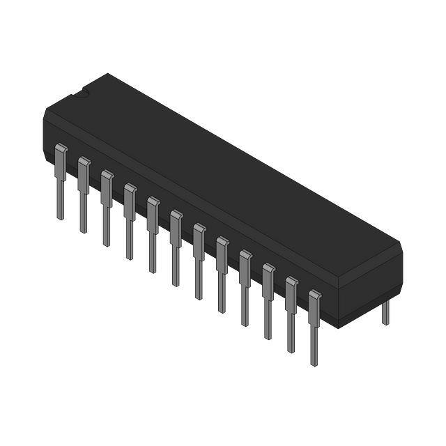
is packaged in a 24-pin plastic DIP rated for the –40°C
to +85°C extended industrial temperature range.
16 +VREF Out
+VL
6
15 Inv In
+VS 10
–VS
7
AGND
8
DGND
1
10V
Ref
10kΩ
A3
12 Inv Out
11 VREF In
20kΩ
19 BPO A
20kΩ
DAC A
A1
Serial
Data and
Control In
Logic
14 VOUT A
20kΩ
18 BPO B
High-stability laser-trimmed thin film resistors assure
high reliability and true 12-bit integral and differential
linearity over the full specified temperature range.
20kΩ
DAC B
A2
Serial
Data
Out
SBAS008
10kΩ
17 VOUT B
5
International Airport Industrial Park • Mailing Address: PO Box 11400
Tel: (520) 746-1111 • Twx: 910-952-1111 • Cable: BBRCORP •
• Tucson, AZ 85734 • Street Address: 6730 S. Tucson Blvd. • Tucson, AZ 85706
Telex: 066-6491 • FAX: (520) 889-1510 • Immediate Product Info: (800) 548-6132
© 1991 Burr-Brown Corporation
PDS-1103B
Printed in U.S.A. October, 1993
�SPECIFICATIONS, Guaranteed over TA = –40°C to +85°C unless otherwise specified.
ELECTRICAL
Specifications as shown for VS = ±12V or ±15V, VL = +5V, and RL = 2kΩ unless otherwise noted.
DAC2814AP
PARAMETER
CONDITIONS
DIGITAL INPUTS
Resolution
VIH (Input High Voltage)
VIL (Input Low Voltage)
IIN ( Input Current)
MIN
12
+2
0
ACCURACY
Integral, Relative Linearity (1)
Differential Nonlinearity (2)
Unipolar Offset Error
Bipolar Zero Error
Gain Error Unipolar, Bipolar
Power Supply Sensitivity (3)
ISINK = 1.6mA
ISOURCE = 500µA
0
+2.4
+9.980
±5
±0.1
±5
±30
±5
±15
+10
±2
+10.020
±30
Bits
V
V
µA
µA
pF
*
*
V
V
±1/2
*
±1
±0.5
*
±10
±0.15
*
LSB
LSB
LSB
mV
mV
mV
%
ppmFSR/V
*
*
*
±20
*
±8
ppm/°C
ppmFSR/°C
ppmFSR/°C
*
*
+10.015
±20
*
*
40
*
V
ppm/°C
mA
mA
pF
mA
ppm/mA
±5
*
ppm/V
–9.985
±20
V
ppm/°C
Ω
mA
pF
mA
+10/–5
+6.5/–5
+9.985
*
*
500
±20
–10.020
–10
*
*
–9.980
±30
–10.015
0.1
*
200
±30
3.5
7
14
*
*
±7
*
*
5
10
20
*
*
*
*
*
*
±10
–VS + 1.4
+VS – 1.4
*
*
0.1
CL = 100pF
To 1/2 LSB of Full Scale
To 1/2 LSB of Full Scale
2.5
3.5
10
3
Full Scale Transition
CL= 100pF
®
2
V
Ω
mA
pF
mA
*
*
µs
µs
V/µs
MHz
*
500
±30
*
*
10
10
*
*
*
*
kΩ
kΩ
kΩ
V
*
*
±5
VOUT
D/A GLITCH IMPULSE
DAC2814
*
*
*
*
*
*
*
±1
±3
±20
±0.2
30
ANALOG GROUND CURRENT
(Code Dependent)
DIGITAL CROSSTALK
UNITS
+1.5/–1
REFERENCE INPUT
Reference Input Resistance
Inverter Input Resistance
BPO Input Resistance
Reference Input Range
DYNAMIC PERFORMANCE(5)
Unipolar Mode Settling Time
Bipolar Mode Settling Time
Slew Rate
Small-Signal Bandwidth
MAX
*
+0.4
+5
With Internal or External 10.0V Ref
VS = ±11.4V to ±18V
VL = +4.5V to +5.5V
TA = 25°C
TA = –40°C to +85°C
TYP
±1
±1
TA = 25°C
TA = –40°C to +85°C
TA = +25°C
TA = –40°C TO +85°C
Max Load Capacitance (For Stability)
Short Circuit Current
Load Regulation
(∆ VOUT vs ∆ ILOAD)
Supply Regulation
(∆ VOUT vs ∆ VS)
INVERTER
–10V Reference(4), Inverter Output
–10V Reference Drift
DC Output Impedance
Output Current
Max Load Capacitance (For Stability)
Short Circuit Current
ANALOG SIGNAL OUTPUTS
Voltage Range
DC Output Impedance
Output Current
Max Load Capacitance (For Stability)
Short Circuit Current
MIN
0.8
TEMPERATURE DRIFT
Gain Drift Unipolar, Bipolar
Unipolar Offset Drift
Bipolar Zero Drift
REFERENCE OUTPUT
Output Voltage
Reference Drift
Output Current
DAC2814BP
MAX
+5
+0.8
±1
±10
TA = 25°C
TA = –40°C to +85°C
CIN (Input Capacitance)
DIGITAL OUTPUT
Data Out VOL
VOH
TYP
±2
*
mA
3
*
nV-s
30
*
nV-s
�SPECIFICATIONS
(CONT), Guaranteed over TA = –40°C to +85°C unless otherwise specified.
ELECTRICAL
Specifications as shown for VS = ±12V or ±15V, VL = +5V, and RL = 2kΩ unless otherwise noted.
DAC2814AP
PARAMETER
POWER SUPPLY
+VS and –VS
+VL
+IS
–IS
+IL
+IL
Total Power, All DACs
CONDITIONS
TYP
MAX
MIN
TYP
MAX
UNITS
±11.4
4.5
±15
5
+10
–10
0.2
±18
5.5
+13.5
–13.5
1
5
410
*
*
*
*
*
*
*
*
*
*
*
*
*
*
V
V
mA
mA
mA
mA
mW
+85
+85
*
*
*
*
°C
°C
°C/W
Digital Inputs = 0V or +VL
Digital Inputs = VIL or VIH
TEMPERATURE RANGE
Specified
Operating
Thermal Resistance θJA
DAC2814BP
MIN
300
–40
–40
*
75
*
NOTES: (1) End point linearity. (2) Guaranteed monotonic. (3) Change in bipolar full scale output. Includes voltage output DAC, voltage reference, and reference
inverter. (4) Inverter output with inverter input connected to +VREF. (5) Guaranteed but not tested.
ABSOLUTE MAXIMUM RATINGS
PACKAGE INFORMATION
+VL to AGND ................................................................................. 0V, +7V
+VL to DGND ................................................................................ 0V, +7V
+VS to AGND .............................................................................. 0V, +18V
–VS to AGND ............................................................................... 0V,–18V
AGND to DGND ................................................................................ ±0.3V
Any digital input to DGND .............................................. –0.3V, +VL +0.3V
Ref In to AGND .................................................................................. ±25V
Ref In to DGND .................................................................................. ±25V
Storage Temperature Range .......................................... –55°C to +125°C
Operating Temperature Range ......................................... –40°C to +85°C
Lead Temperature (soldering, 10s) ................................................ +300°C
Junction Temperature .................................................................... +155°C
Output Short Circuit ................................... Continuous to common or ±VS
Reference Short Circuit .............................. Continuous to common or +VS
MODEL
DAC2814AP
DAC2814BP
PACKAGE
PACKAGE DRAWING
NUMBER(1)
24-Pin Plastic DIP
24-Pin Plastic DIP
167
167
NOTE: (1) For detailed drawing and dimension table, please see end of data
sheet, or Appendix D of Burr-Brown IC Data Book.
ELECTROSTATIC
DISCHARGE SENSITIVITY
Electrostatic discharge can cause damage ranging from
performance degradation to complete device failure. BurrBrown Corporation recommends that all integrated circuits be
handled and stored using appropriate ESD protection
methods.
The information provided herein is believed to be reliable; however, BURR-BROWN assumes no responsibility for inaccuracies or omissions. BURR-BROWN assumes
no responsibility for the use of this information, and all use of such information shall be entirely at the user’s own risk. Prices and specifications are subject to change
without notice. No patent rights or licenses to any of the circuits described herein are implied or granted to any third party. BURR-BROWN does not authorize or warrant
any BURR-BROWN product for use in life support devices and/or systems.
®
3
DAC2814
�PIN DESIGNATIONS
PIN
1
2
3
4
5
6
7
8
9
10
11
12
DESCRIPTOR
FUNCTION
PIN
DESCRIPTOR
FUNCTION
DGND
LATCH B
CLR
MODE
Data Out
+VL
–VS
AGND
NC
+VS
VREF In
Inv Out
Digital common
Latch data update, logic input, DAC B
Asychronous input reset to zero
Selection input for unipolar or bipolar reset to zero
Serial data output
Positive logic power supply, +5V input
Negative analog power supply , –15V input
Analog common
No internal connection
Positive analog power supply, +15V input
± Reference voltage input
Inverter (A3) output
24
23
22
21
20
19
18
17
16
15
14
13
CS
Data In
LATCH A
CLK
NC
BPO A
BPO B
VOUT B
+VREF Out
Inv In
VOUT A
NC
Chip select enable, DAC A and DAC B
Serial data input
Latch data update, logic input, DAC A
Clock input
No internal connection
Bipolar offset input, DAC A
Bipolar offset input, DAC B
Analog output voltage, DAC B
Reference voltage, +10V output
Inverter (A3) input
Analog output voltage, DAC A
No internal connection
PIN CONFIGURATIONS
Top View
DGND
1
24 CS
LATCH B
2
23 Data In
CLR
3
22 LATCH A
MODE
4
21 CLK
Data Out
5
20 NC
DAC2814
+VL
6
–VS
7
18 BPO B
AGND
8
17 VOUT B
NC
9
16 +VREF Out
19 BPO A
+VS 10
15 Inv In
VREF In
11
14 VOUT A
Inv Out
12
13 NC
NC = No Internal Connection
TYPICAL PERFORMANCE CURVES
TA = +25°C, V S = ±12V or ±15V, VL = +5V unless otherwise noted.
NOISE vs BANDWIDTH (Bipolar Mode)
PSRR vs FREQUENCY (Bipolar Mode)
250
80
Voltage Noise (µVrms)
70
PSRR (dB)
60
50
40
VOUT = 0V
30
20
200
150
VOUT = +10V
FFFHEX
100
50
VOUT = +10V
10
VOUT = 0V
800HEX
0
0
1k
10k
100k
100
1M
Frequency (Hz)
10k
Frequency (Hz)
®
DAC2814
1k
4
100k
1M
�TYPICAL PERFORMANCE CURVES (CONT)
TA = +25°C, VS = ±12V or ±15V, VL = +5V unless otherwise noted.
POWER SUPPLY CURRENT vs TEMPERATURE
+0.005
Bipolar Zero
0
0
–0.5
–0.005
Bipolar Offset
–1.0
–1.5
–40
–20
±IS (mA) Analog Supply
+0.5
0
20
40
60
+IL (All Logic Inputs = 2V)
11.6
+0.01
Gain Error
∆ Gain Error (%)
+1.0
1.4
11.8
1
11.4
11.2
0.8
IS
0.6
11
0.4
10.8
–0.01
10.6
–0.015
10.4
80
1.2
+IL (All Logic Inputs = 0V or VL)
+IL (mA) Logic Supply
+0.015
+1.5
0.2
0
–40
Temperature (°C)
–20
0
20
40
60
80
Temperature (°C)
CROSSTALK (Bipolar Mode)
OUTPUT VOLTAGE SWING vs RESISTOR LOAD
25
VS = ±15V
10V REF
0V
VL = 5V
15
VOUT B
VOUT
VOUT (Vp-p)
20
VOUT A
10
LATCH A
+5V
5
0V
0
Time (500ns/div)
10
100
1k
10k
NOTE: Crosstalk is dominated by digital crosstalk/
feedthrough of the LATCH signal.
Load Resistance (Ω )
FULL-SCALE OUTPUT SWING
BIPOLAR (20V Step)
FULL-SCALE OUTPUT SWING
UNIPOLAR (10V Step)
0V
VOUT (5V/div)
VOUT (5V/div)
∆ Bipolar Offset and Zero Error (mV)
CHANGE OF GAIN, BIPOLAR OFFSET AND ZERO ERROR
vs TEMPERATURE
VOUT
0V
VOUT
LATCH
+5V
0V
Time (2µs/div)
Time (2µs/div)
®
5
DAC2814
�TYPICAL PERFORMANCE CURVES (CONT)
TA = +25°C, VS = ±12V or ±15V, VL = +5V unless otherwise noted.
VOUT
–10V
+10V
VOUT
+5V
LATCH
0V
0V
Time (2µs/div)
SETTLING TIME
UNIPOLAR (+10V to 0V STEP)
SETTLING TIME
UNIPOLAR (0V to +10V Step)
0V
VOUT
LATCH
+5V
0V
+10V
VOUT
+5V
LATCH
0V
Time (1µs/div)
Time (1µs/div)
MAJOR CARRY GLITCH
DIGITAL FEEDTHROUGH
0V
VOUT (5mV/div)
VOUT (20mV/div)
LATCH
+5V
Time (1µs/div)
∆V Around +10V (1mV/div)
∆V Around 0V (1mV/div)
SETTLING TIME
BIPOLAR (+10V to –10V Step)
∆V Around –10V (2mV/div)
∆V Around +10V (2mV/div)
SETTLING TIME
BIPOLAR (–10V to +10V)
VOUT
+5V
LATCH
0V
VOUT
0V
Time (1µs/div)
Time (500ns/div)
NOTE: Data transition 800HEX to 7FFHEX.
DAC output noise due to activity on digital inputs
with latch disabled.
®
DAC2814
6
�TIMING CHARACTERISTICS
VL = +5V, TA = –40°C to +85°C.
t5
PARAMETER
MINIMUM
CLK
15ns
15ns
15ns
Data
t1—Data Setup Time
t2—Data Hold time
t3—Chip Select to CLK,
Latch, Data Setup Time
t4—Chip Select to CLK,
Latch, Data Hold Time
t5—CLK Pulse Width
t6—Clear Pulse Width
t7—Latch Pulse Width
t8—CLK Edge to LATCH A
or LATCH B
0V
t1
t3
5V
0V
t2
5V
CS
t8
40ns
t7
t4
LATCH A
LATCH B
40ns
40ns
40ns
15ns
5V
t6
5V
CLR
NOTES: (1) All input signal rise and fall times are measured from 10% to 90% of +5V • t R = tF = 5ns.
(2) Timing measurement reference level is VIH + VIL .
2
INTERFACE LOGIC TRUTH TABLE
MODE
CLR
CLK
CS
LATCH A
LATCH B
X
X
X
X
X
0
1
1
1
1
1
1
0
0
↓
X
X
X
X
X
X
0
1
0
0
0
X
X
X
X
0
1
0
X
X
X
X
1
0
0
X
X
NOTE: X = Don’t care
FUNCTION
Data Clocked In
No Data Transfer
DAC A Register Updated
DAC B Register Updated
DAC A and DAC B Updated Together
All Registers Cleared
Shift Registers Cleared = 000HEX, DAC Registers = 800HEX
↓ = Falling edge triggered.
FUNCTIONAL BLOCK DIAGRAM , DAC2814 — Dual, 12-bit DAC, Serial Port
Data In
VREF In
23
11
20kΩ
19 BPO A
LATCH A 22
LATCH B
12-Bit
Shift
Register
2
20kΩ
0-11
12-Bit
Latch
Register
Bits 0-11
DAC A
A1
Bit 11
CLK 21
14 VOUT A
20kΩ
18 BPO B
Control
Logic
12-Bit
Shift
Register
CS 24
CLR
MODE
20kΩ
0-11
12-Bit
Latch
Register
DAC B
Bits 0-11
A2
3
17 VOUT B
10kΩ
10kΩ
+10V
Voltage
Reference
4
A3
12 Inv Out
Bit 11
5
8
6
10
7
Data Out
AGND
+VL
+VS
–VS
1
16
15
DGND +VREF Out Inv In
®
7
DAC2814
�DISCUSSION OF
SPECIFICATIONS
DIGITAL CROSSTALK
Digital crosstalk is the glitch impulse measured at the output
of one DAC due to a full scale transition on the other
DAC—see Typical Performance Curves. It is dominated by
digital coupling. Also, the integrated area of the glitch pulse
is specified in nV–s. See table of electrical specifications.
INPUT CODES
All digital inputs of the DAC2814 are TTL and 5V CMOS
compatible. Input codes for the DAC2814 are either USB
(Unipolar Straight Binary) or BOB (Bipolar Offset Binary)
depending on the mode of operation. See Figure 3 for ±10V
bipolar connection. See Figures 4 and 5 for 0 to 10V and 0
to –10V unipolar connections.
DIGITAL FEEDTHROUGH
Digital feedthrough is the noise at a DAC output due to
activity on the digital inputs—see Typical Performance
Curves.
UNIPOLAR AND BIPOLAR
OUTPUTS FOR SELECTED INPUT
DIGITAL INPUT
FFFHEX
800HEX
7FFHEX
000HEX
OPERATION
UNIPOLAR (USB)
BIPOLAR (BOB)
+Full scale
+1/2 Full scale
+1/2 Full scale – 1 LSB
Zero
+Full scale
Zero
Zero – 1 LSB
–Full scale
DACs can be updated simultaneously or independently as
required. Data are transferred on falling clock edges into a
24-bit shift register. DAC B MSB is loaded first. Data are
transferred to the DAC registers when the LATCH signals
are brought low. The data are latched when the LATCH
signals are brought high. Both LATCH signals may be tied
together to allow simultaneous update of the DACs if required. The output of the DAC shift register is provided to
allow cascading of several DACS on the same bit stream.
By using separate signals for LATCH A and LATCH B, it
is possible to update either one of the two DACs every 12
clock cycles.
When CLR is brought low, the input shift registers are
cleared to 000HEX, while the DAC registers = 800HEX. If
LATCH is brought low after CLR, the DACs are updated
with 000HEX resulting in –10V (Bipolar) or 0V (Unipolar) on
the output.
INTEGRAL OR RELATIVE LINEARITY
This term, also know as end point linearity, describes the
transfer function of analog output to digital input code.
Integral linearity error is the deviation of the analog output
versus code transfer function from a straight line drawn
through the end points.
DIFFERENTIAL NONLINEARITY
Differential nonlinearity is the deviation from an ideal 1
LSB change in the output voltage when the input code
changes by 1 LSB. A differential nonlinearity specification
of ±1 LSB maximum guarantees monotonicity.
CIRCUIT DESCRIPTION
UNIPOLAR OFFSET ERROR
The output voltage for code 000HEX when the DAC is in
unipolar mode of operation.
Each of the two DACs in the DAC2814 consists of a CMOS
logic section, a CMOS DAC cell, and an output amplifier.
One buried-zener +10.0V reference and a reference inverter
(for a –10.0V reference) are shared by both DACs.
Figure 1 is a simplified circuit for a DAC cell. An R, 2R
ladder network is driven by a voltage reference at VREF.
Current from the ladder is switched either to IOUT or AGND
by 12 single-pole double-throw CMOS switches. This maintains constant current in each leg of the ladder regardless of
digital input code. This makes the resistance at VREF constant (it can be driven by either a voltage or current reference). The reference can be either positive or negative
polarity with a range of up to ±10V.
BIPOLAR ZERO ERROR
The output voltage for code 800HEX when the DAC is in the
bipolar mode of operation.
GAIN ERROR
The deviation of the output voltage span (VMAX – VMIN)
from the ideal span of 10V – 1 LSB (unipolar mode) or 20V
– 1 LSB (bipolar mode). The gain error is specified with and
without the internal +10V reference error included.
R
OUTPUT SETTLING TIME
R
R
VREF
The time required for the output voltage to settle within a
percentage-of-full-scale error band for a full scale transition.
Settling to ±0.012% (1/2 LSB) is specified for the DAC2814.
2R
2R
2R
2R
R
R FB
IOUT
DIGITAL-TO-ANALOG GLITCH
D11
(MSB)
Ideally, the DAC output would make a clean step change in
response to an input code change. In reality glitches occur
during the transition. See Typical Performance Curves.
D10
D9
D0
(LSB)
AGND
FIGURE 1. Simplified Circuit Diagram of DAC Cell.
®
DAC2814
2R
8
�DAC2814
DAC2814
DAC A
DAC A
VOUT A
VOUT A
DAC B
DAC B
VOUT B
VOUT B
AGND
AGND
R GND
R GND
NOTE: Ideally RGND = 0Ω
FIGURE 2. Recommended Ground Connections for Multiple DAC packages.
OUTPUT RANGE CONNECTIONS
CMOS switches included in series with the ladder terminating resistor and the feedback resistor, RFB, compensate for
the temperature drift of the ladder switch ON resistance.
±10V Output Range
For a ±10V bipolar outputs connect the DAC2814 as shown
in Figure 3. Connect the MODE to logic high (+5V) for reset
to bipolar zero. With MODE connected low (GND) reset
will be to –Full-Scale.
The output op amps are connected as transimpedance amplifiers to convert the DAC-cell output current into an output
voltage. They have been specially designed and compensated for precision and fast settling in this application.
0 To +10V Output Range
For 0 to +10V unipolar outputs connect the DAC2814 as
shown in Figure 4. Connect the MODE to logic low (GND)
for reset to unipolar zero.
POWER SUPPLY CONNECTIONS
The DAC2814 is specified for operation with power supplies of VL = +5V and VS = either ±12V or ±15V. Even with
the VS supplies at ±11.4V the DACs can swing a full ±10V.
Power supply decoupling capacitors (1µF tantalum) should
be located close to the DAC power supply connections.
0 To –10V Output Range
For 0 to –10V unipolar outputs connect the DAC2814 as
shown in Figure 5. Connect the MODE to logic low (GND)
for reset to unipolar zero.
Separate digital and analog ground pins are provided to
permit separate current returns. They should be connected
together at one point. Proper layout of the two current
returns will prevent digital logic switching currents from
degrading the analog output signal. The analog ground
current is code dependent so the impedance to the system
reference ground must be kept to a minimum. Connect
DACs as shown in Figure 2 or use a ground plane to keep
ground impedance less than 0.1Ω for less than 0.1LSB error.
CONNECTION TO DIGITAL BUS
Cascaded Bus Connection
Multiple DAC2814s can be connected to the same CLK and
DATA input lines in two ways. Since the output of the DAC
shift register is available, any number of DAC2814s can be
cascaded on the same input bit stream as shown in Figure 6.
This arrangement allows all DACs in the system to be
updated simultaneously and requires a minimum number of
control signal inputs. However, up to 24N CLK cycles may
be required to update any given DAC, where
N = number of DAC2814s.
–10V REFERENCE
An internal inverting amplifier (Gain = –1.0V/V) is provided to invert the +10V reference. Connect +VREF Out to
Inv In for a –10V reference at Inv Out.
Parallel Bus Connection
Several DAC2814s can also have their DATA inputs connected in parallel as shown in Figure 7. This allows any
DAC in the system to be updated in a maximum of 24 CLK
cycles.
®
9
DAC2814
�+5V
6
DAC2814
16
+
1µF
10kΩ
10
+15V
1µF
10V
Ref
+
10kΩ
A3
12
7
–15V
1µF
15
+
11
20kΩ
19
20kΩ
DAC A
A1
Serial
Data and
Control In
20kΩ
14
VOUT A
18
20kΩ
DAC B
A2
MODE 4
1
VOUT B
8
DGND
+5V
17
AGND
FIGURE 3. Analog Connections for ±10V DAC Output.
+5V
6
DAC2814
16
+
1µF
10kΩ
10
+15V
1µF
+
10V
Ref
10kΩ
A3
12
7
–15V
1µF
15
+
11
20kΩ
19
20kΩ
DAC A
A1
Serial
Data and
Control In
20kΩ
14
VOUT A
18
20kΩ
DAC B
A2
MODE 4
1
8
DGND
FIGURE 4. Analog Connections for 0 to +10V DAC Output.
®
DAC2814
10
AGND
17
VOUT B
�+5V
6
DAC2814
+
1µF
10
+15V
1µF
16
7
–15V
1µF
10V
Ref
+
+
11
20kΩ
19
20kΩ
DAC A
14
A1
Serial
Data and
Control In
20kΩ
VOUT A
18
20kΩ
DAC B
17
A2
MODE 4
1
VOUT B
8
DGND
AGND
FIGURE 5. Analog Connections for 0 to –10V DAC Output.
Multiple DAC2814s Cascaded
Data
LATCH
23
22
2
CLK
21
23
22
2
21
23
22
2
21
Data In
CS
Multiple DAC2814s Paralleled
24
Data
LATCH A
LATCH 1
Data In
Data Out
CS
5
CLK
24
LATCH 2
Data Out
CS
5
21
24
23
LATCH A
LATCH 3
22
2
LATCH B
CLK
22
2
LATCH B
Data In
21
23
LATCH A
CLK
22
2
LATCH B
CLK
23
Data Out
5
21
To Other DACs
Data In
CS
24
LATCH A
LATCH B
CLK
Data In
Data Out
CS
5
24
LATCH A
LATCH B
CLK
Data In
Data Out
CS
5
24
LATCH A
LATCH B
CLK
Data Out
5
FIGURE 7. Parallel Bus Connection for Multiple DAC
packages.
FIGURE 6. Cascaded Serial Bus Connection for Multiple
DAC packages.
®
11
DAC2814
�IMPORTANT NOTICE
Texas Instruments and its subsidiaries (TI) reserve the right to make changes to their products or to discontinue
any product or service without notice, and advise customers to obtain the latest version of relevant information
to verify, before placing orders, that information being relied on is current and complete. All products are sold
subject to the terms and conditions of sale supplied at the time of order acknowledgment, including those
pertaining to warranty, patent infringement, and limitation of liability.
TI warrants performance of its semiconductor products to the specifications applicable at the time of sale in
accordance with TI’s standard warranty. Testing and other quality control techniques are utilized to the extent
TI deems necessary to support this warranty. Specific testing of all parameters of each device is not necessarily
performed, except those mandated by government requirements.
Customers are responsible for their applications using TI components.
In order to minimize risks associated with the customer’s applications, adequate design and operating
safeguards must be provided by the customer to minimize inherent or procedural hazards.
TI assumes no liability for applications assistance or customer product design. TI does not warrant or represent
that any license, either express or implied, is granted under any patent right, copyright, mask work right, or other
intellectual property right of TI covering or relating to any combination, machine, or process in which such
semiconductor products or services might be or are used. TI’s publication of information regarding any third
party’s products or services does not constitute TI’s approval, warranty or endorsement thereof.
Copyright 2000, Texas Instruments Incorporated
�