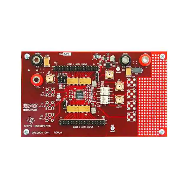
DAC290x-EVM
SBAU071B – JUNE 2001 – REVISED SEPTEMBER 2005
FEATURES
DESCRIPTION
● POPULATED EVALUATION BOARD FOR THE
DUAL, HIGH-SPEED DAC290x
The DAC290x-EVM is designed for ease of use in evaluating the DAC290x dual, high-speed Digital-to-Analog Converter (DAC) family. This family consists of three 125MSPS
DACs: the 10-bit DAC2900, the 12-bit DAC2902, and the
14-bit DAC2904. Due to its flexible design, the user can
evaluate the converter with different clock configurations,
independent bias control, internal or external reference source,
and single- or dual-supply operation. The analog output of
the DAC290x DACs can be configured to drive a 50Ω
terminated cable using a single-ended, or 4:1 or 1:1 impedance ratio transformer.
● PROVIDES FAST AND EASY PERFORMANCE
TESTING FOR THE DAC290x
● SINGLE-ENDED OR TRANSFORMER-COUPLED
DIFFERENTIAL OUTPUTS
● SINGLE CLOCK INPUT CONFIGURATION
● ADJUSTABLE BIAS
Please be aware that an important notice concerning availability, standard warranty, and use in critical applications of
Texas Instruments semiconductor products and disclaimers thereto appears at the end of this data sheet.
All trademarks are the property of their respective owners.
Copyright © 2001-2005, Texas Instruments Incorporated
PRODUCTION DATA information is current as of publication date.
Products conform to specifications per the terms of Texas Instruments
standard warranty. Production processing does not necessarily include
testing of all parameters.
www.ti.com
�INITIAL CONFIGURATION
INTERNAL REFERENCE OPERATION
By using jumpers and 0Ω resistors, the DAC290x-EVM can
be set up in a variety of configurations to accommodate a
specific mode of operation. Before starting evaluation, the
user should decide on the configuration and make the appropriate connections or changes. The demonstration board
comes with the following factory-set configuration:
The full-scale output current is set by applying an external
resistor (R15 and R16) between the FAS1 and FAS2 pins of
the DAC290x and ground. The full-scale output current can
be adjusted from 20mA down to 2mA by varying R15 and
R16 or changing the externally applied reference voltage.
The full-scale output current, IOUTFS, is defined as follows:
• Single clock source driving CLK_1, WRT_1, CLK_2, and
WRT_2 from WRT_1 input J5. W10, R21, R32-R37, and
J6-J8 not installed.
IOUTFS = 32 • (VREF_IN/RBIAS)
• Transformer coupled outputs (1:1) using transformer T1
and T2. R43-R46, C12, C13, C22, and C23 not installed.
Note that a dc-bias voltage is set at the center tap.
• The converter is set to operate with the internal reference.
Jumper W1 is not installed.
• The full-scale output current of both DACs is set to 20mA
through the FSA resistors R15 and R16 (2kΩ each). Jumper
W2 is installed connecting pin 42 (GSET) to ground.
• The DAC290x output is enabled (power-down mode disabled). Jumper W6 is installed connecting pin 37 (PD) to
ground.
POWER SUPPLY
The DAC290x converter requires two power supplies—an
analog and a digital supply. Each of the supplies may be set
independently between +3.0V and +5.0V. The analog supply, +VA, must be connected at banana jack J9 with the
return going to banana jack J10. The digital supply, +VD,
connects at banana jack J11 with the return connected to J12.
When operating the DAC290x with a +3.0V digital supply,
care must be taken that the amplitude of the digital data
inputs has a corresponding logic level. The logic high level
must not exceed the power supply by more than 0.3V. Refer
to the product data sheets (DAC2900—SBAS166;
DAC2902—SBAS167; DAC2904—SBAS198) for further
details.
All analog and digital power, and grounds are distributed by
the use of power planes.
where VREF_IN is the voltage at pin REF_IN and RBIAS is the
resistance of R15 (for DAC1) or R16 (for DAC2). This
voltage is typically +1.25V when using the internally provided reference voltage source. Two potentiometers (R40
and R41) are provided to allow the user to adjust the center
voltage of the DAC outputs across transformers T1 and T2.
The EVM initial setup is for full-scale output current operation, with the potentiometers adjusted to provide 0.5V at the
center tap of the transformers.
EXTERNAL REFERENCE OPERATION
The internal reference can be disabled and overridden by an
external reference. Two methods of external reference are
provided by the EVM. The user can provide an external
reference by connecting a voltage source to SMA connector
J13 with Jumper W1 installed between pins 2 and 3. In
addition, a reference circuit has been included on the EVM
to provide a second external reference source. This source is
available by placing Jumper W1 between pins 1 and 2 and
adjusting potentiometer R7 to the desired voltage. The range
of this circuit is from 0V to 1.25V. The specified range for
external reference voltages should never exceed the limits as
specified per the data sheet.
POWER-DOWN MODE
The DAC290x-EVM provides a means of placing the
DAC290x converter into a power-down mode. This mode is
activated by re-configuring Jumper W6 so that it connects
the PD-pin (pin 37) to +VD.
INPUT DATA
INPUT CLOCK
The DAC290x-EVM default configuration requires only
one clock input. The clock should be applied via SMA
connector WRT_1 (J5), which provides a 50Ω terminated
input. It is recommended to use a square wave clock with an
amplitude of ≥ 3.0Vp-p. In order to preserve the specified
performance of the DAC290x converter, the clock source
should feature very low jitter.
The DAC290x-EVM allows the user to input I and Q digital
data to the DAC using J1 and J2. The board provides series
dampening 22Ω resistors and buffering to minimize digital
ringing and switching noise. The connectors also provide a
path for an input clock. With the EVM set up in the single
clock source mode, the user can provide a clock through J1
or J2 by installing jumper W10 and resistor R21. The 14-bit
input data buses are brought in through two 34-pin headers
as shown in Tables I and II.
MULTIPLE INPUT CLOCKS
The DAC290x-EVM evaluation board can be configured for
multiple input clocks, each driving a CLK or WRT input pin.
This mode would require the user to install J6, J7, J8, R32
through R37, and removal of R22 through R25.
2
DAC290x-EVM
SBAU071B
�J1 PIN #
DESCRIPTION
J1 PIN #
DESCRIPTION
J2 PIN #
DESCRIPTION
J2 PIN #
1
2
3
4
5
6
7
8
9
10
11
12
13
14
15
16
17
Data Bit 13 (MSB)
GND
Data Bit 12
GND
Data Bit 11
GND
Data Bit 10
GND
Data Bit 9
GND
Data Bit 8
GND
Data Bit 7
GND
Data Bit 6
GND
Data Bit 5
18
19
20
21
22
23
24
25
26
27
28
29
30
31
32
33
34
GND
Data Bit
GND
Data Bit 3
GND
Data Bit 2
GND
Data Bit 1
GND
Data Bit 0
GND
Open
GND
Open
GND
CLK1
GND
1
2
3
4
5
6
7
8
9
10
11
12
13
14
15
16
17
Data Bit 13 (MSB)
GND
Data Bit 12
GND
Data Bit 11
GND
Data Bit 10
GND
Data Bit 9
GND
Data Bit 8
GND
Data Bit 7
GND
Data Bit 6
GND
Data Bit 5
18
19
20
21
22
23
24
25
26
27
28
29
30
31
32
33
34
TABLE I. Input Connector J1—Data Port 1.
GND
Data Bit
GND
Data Bit
GND
Data Bit
GND
Data Bit
GND
Data Bit
GND
Open
GND
Open
GND
CLK2
GND
4
3
2
1
0
TABLE II. Input Connector J2—Data Port 2.
VALUE
FOOTPRINT
QTY
PART NUMBER
VENDOR
REF DESIGNATOR
47µF, Tantalum, 10%, 10V Cap
0.1µF, 100V, 10% Capacitor
0.1µF,16V, 10% Capacitor
10µF, 10V, 10% Capacitor
0.01µF, 100V, 5% Capacitor
1.0µF, 16V, 10% Capacitor
22pF, 50V, 5%, Capacitor
Ferrite Bead
24.9Ω Resistor, 1/16W, 1%
22.1Ω Resistor, 1/16W, 1%
49.9Ω Resistor, 1/16W, 1%
2.0KΩ Resistor, 1/8W, 1%
1.0KΩ Resistor, 1/8W, 1%
100Ω Resistor, 1/4W, 1%
0Ω Resistor, 1/16W, 1%
7343
805
603
3528
805
1206
603
27—037447
603
603
603
805
805
805
603
2
3
7
3
2
2
0
2
2
2
5
2
2
2
5
10TPA47M
08055C104JAT2A
ECJ-1VB1C104K
GRM42X5R106K10
12065C103KAT2A
1206ZC105KAT2A
06035A220JAT2A
#27-037447
ERJ-3EKF24R9V
ERJ-3EKF22R1V
ERJ-3EKF49R9V
CRCW08052001F
CRCW08051001F
CRCW08051000F
ERJ-3EKF0R00V
SANYO
AVX
Panasonic
Murata
AVX
AVX
AVX
FairRite
Panasonic
Panasonic
Panasonic
Dale
Dale
Dale
Panasonic
C30 C36
C6 C28 C34
C7 C11 C14 C19 C20 C21 C24
C5 C26 C32
C29 C35
C27 C33
1206
BOURNS_32X4W
MC_KK81
SMA_Jack
Test_Point
3-Pos_Jumper
NA
34-Pin Header
BANANA_JACK
BANANA_JACK
48-TQFP(PFB)
8-SOP(D)
2NBS16
8-MSOP(DGK)
4-40 Screw
4
3
2
4
3
5
0
2
2
2
1
1
4
1
4
0Ω Resistor, 1/10W, 1%
500Ω Pot
Transformer
SMA Connectors
Black Test Point
3-Pos_Header
2 Circuit Jumpers
34-Pin Header
Red Banana Jacks
Black Banana Jacks
DAC29XX
LT1004D-1.2
22Ω R-Pack
TLV2462
Stand Off Hex (1/4 x 1 inch)
DESCRIPTION
ERJ-6ENF0R00V
Panasonic
3214W-501ECT
Bourns
T1-1T-KK8
Mini-Circuits
713-4339 (901-144-8RFX)
ALLIED
5001K
Keystone
TSW-150-07-L-S
Samtec
863-3285
Allied(molex)
TSW-117-07-L-D
Samtec
ST-351A
ALLIED
ST351B
ALLIED
DAC2900/02/04Y
TI
LT1004ID-1-2
TI
4816P-001-220
Bourns
TLV2462CDGK
TI
219-2063
Allied
NOT INSTALLED
C12 C13 C22 C23
FB1 FB2
R20 R30
R14 R31
R17 R18 R27 R28 R38
R15 R16
R5 R9
R19 R29
R22 R23 R24 R25 R26
R10 R11 R12 R13
R7 R40 R41
T1 T2
J3 J4 J5 J13
TP1 TP2 TP3
W1 W2 W5 W6 W10
R32, R34, R36
R21 R33 R35 R37 R43
R44 R45 R46
J14 J15 J16 J17 J6 J7 J8
J1 J2
J9 J11
J10 J12
U5
U2
R1 R2 R3 R4
U4
TABLE III. DAC290x-EVM Parts List.
DAC290x-EVM
SBAU071B
3
�FIGURE 1. DAC290x-EVM Circuit Schematic #1.
33
31
29
27
25
23
21
19
17
15
13
11
9
7
5
3
1
NOTES:
33
31
29
27
25
23
21
19
17
15
13
11
9
7
5
3
1
22
R31
D0_2
D1_2
D2_2
D3_2
D4_2
D5_2
D6_2
D7_2
D8_2
D9_2
D10_2
D11_2
D12_2
D13_2
D0_1
D1_1
D2_1
D3_1
D4_1
D5_1
D6_1
D7_1
D8_1
D9_1
D10_1
D11_1
D12_1
D13_1
22 Ohms
R1
CLK1
CLK2
R4
22 Ohms
R3
22 Ohms
R2
22 Ohms
22
1. PART NOT INSTALLED
34
32
30
28
26
24
22
20
18
16
14
12
10
8
6
4
2
DATA PORT 2
J2
34
32
30
28
26
24
22
20
18
16
14
12
10
8
6
4
2
DATA PORT 1
R14
BD0_2
BD1_2
BD2_2
BD3_2
BD4_2
BD5_2
BD6_2
BD7_2
BD8_2
BD9_2
BD10_2
BD11_2
BD12_2
BD13_2
BD0_1
BD1_1
BD2_1
BD3_1
BD4_1
BD5_1
BD6_1
BD7_1
BD8_1
BD9_1
BD10_1
BD11_1
BD12_1
BD13_1
U2
LT1004D-1.2
1K
500
R7
6
5
7
8
CLK2
CLK1
1
C21
2
W10
C6
BD1_1
BD0_1
WRT_1
J5
0.1uF
DVDD
C20
0.1uF
J13
SMA
W5
2
2
W2
AVDD
U5
DAC290x
1
0 Ohm
(Note 1)
FSA1
BD12_2
BD13_2
BD0_2
BD1_2
BD2_2
BD3_2
BD4_2
BD5_2
BD6_2
BD7_2
BD8_2
BD9_2
BD10_2
BD11_2
1
0 Ohm
R25
(Note 1)
WRT_2
J8
(Note 1)
0 Ohm
R35
49.9
R36 (Note 1)
WRT_2
36
35
34
33
32
31
30
29
28
27
26
25
1
2K
R16
(Note 1)
0 Ohm
49.9
R38
FSA2
R37
POWER DOWN
W6
DVDD
2K
R15
D0_2
D1_2
D2_2
D3_2
D4_2
D5_2
D6_2
D7_2
D8_2
D9_2
D10_2
D11_2
2
(Note 1)
CLK_2
J7
0 Ohm
R24
0 Ohm
R33
49.9
R34 (Note 1)
CLK_2
R26
(Note 1)
CLK_1
J6
0 Ohm
R23
49.9
(Note 1)
R32
WRT_1
D13_1
D12_1
D11_1
D10_1
D9_1
D8_1
D7_1
D6_1
D5_1
D4_1
D3_1
D2_1
0 Ohm
1
3
0.1uF
C7
R22
BD13_1 1
BD12_1 2
BD11_1 3
BD10_1 4
BD9_1
5
BD8_1
6
BD7_1
7
BD6_1
8
BD5_1
9
BD4_1 10
BD3_1 11
BD2_1 12
0.1uF
C11
AVDD
1
W1
EXTIO
(0-1.25V)
.1uF
C19
1K
R9
0 Ohm
(Note 1)
R21
DVDD
.1uF
AVDD
TLV2462D
U4A
TLV2462D
U4B
NOT USED
10uF
+ C5
2
3
2
AVDD
1
3
4
1
3
2
3
4
5
R5
5
4
3
2
CLK_1
5
4
3
2
1
3
1
3
48
47
46
45
44
43
42
41
40
39
38
37
N/C
+VA
IOUT1
IOUT1
FSA1
REF_IN
GSET
FSA2
IOUT2
IOUT2
AGND
PD
D1_1
D0_1
DGND
+VD
WRT_1
CLK_1
CLK_2
WRT_2
DGND
+VD
D13_2
D12_2
13
14
15
16
17
18
19
20
21
22
23
24
5
4
3
2
J1
AVDD
5
4
3
2
R27
49.9
49.9
R17
R19
100
22 pF
(Note 1)
C13
R30
24.9
22pF
(Note 1)
C23
100
R29
500
R41
AVDD
R18
49.9
R28
49.9
22pF
(Note 1)
C22
(Note 1)
22 pF
C12
500
R40
AVDD
0 Ohm
0 Ohm
R13
0 Ohm
R12
0 Ohm
R11
R10
R20
24.9
SMA
T1
6
1
.1uF
C24
R46
0 Ohm
(Note 1)
1
1
2
3
(Note 1)
R43
0 Ohm
.1uF
C14
1
T2
1
6
SMA
(Note 1)
J17
T1-1T-KK81
4
(Note 1)
J16
SMA
3
4
T1-1T-KK81
R45
J15
0 Ohm
SMA (Note 1)
(Note 1)
1
2
1
0 Ohm
R44
(Note 1)
1
(Note 1)
J14
2
3
4
5
2
3
4
5
2
3
4
5
2
3
4
5
J3
IOUT2
J4
IOUT1
2
3
4
5
2
3
4
5
4
DAC290x-EVM
SBAU071B
�FIGURE 2. DAC290x-EVM Circuit Schematic #2.
DAC290x-EVM
SBAU071B
5
J10
TP1
BLACK
J12
BLACK
RED
J11
+VD
BLACK
RED
J9
+VA
VD
TP2
BLACK
VA
1uF
TP3
BLACK
C33
10uF
FB2
C35
0.1uF 0.01uF
C34
+
C30
47 uF
+
C36
47 uF
DVDD
0.1uF 0.01uF
C29
C28
1uF
AVDD
C27
+ C32
10uF
+ C26
FB1
�FIGURE 3. Top Layer with Silkscreen.
FIGURE 4. Ground Plane.
6
DAC290x-EVM
SBAU071B
�FIGURE 5. Power Plane.
FIGURE 6. Bottom Layer with Silkscreen.
DAC290x-EVM
SBAU071B
7
�IMPORTANT NOTICE
Texas Instruments Incorporated and its subsidiaries (TI) reserve the right to make corrections, modifications,
enhancements, improvements, and other changes to its products and services at any time and to discontinue
any product or service without notice. Customers should obtain the latest relevant information before placing
orders and should verify that such information is current and complete. All products are sold subject to TI’s terms
and conditions of sale supplied at the time of order acknowledgment.
TI warrants performance of its hardware products to the specifications applicable at the time of sale in
accordance with TI’s standard warranty. Testing and other quality control techniques are used to the extent TI
deems necessary to support this warranty. Except where mandated by government requirements, testing of all
parameters of each product is not necessarily performed.
TI assumes no liability for applications assistance or customer product design. Customers are responsible for
their products and applications using TI components. To minimize the risks associated with customer products
and applications, customers should provide adequate design and operating safeguards.
TI does not warrant or represent that any license, either express or implied, is granted under any TI patent right,
copyright, mask work right, or other TI intellectual property right relating to any combination, machine, or process
in which TI products or services are used. Information published by TI regarding third-party products or services
does not constitute a license from TI to use such products or services or a warranty or endorsement thereof.
Use of such information may require a license from a third party under the patents or other intellectual property
of the third party, or a license from TI under the patents or other intellectual property of TI.
Reproduction of information in TI data books or data sheets is permissible only if reproduction is without
alteration and is accompanied by all associated warranties, conditions, limitations, and notices. Reproduction
of this information with alteration is an unfair and deceptive business practice. TI is not responsible or liable for
such altered documentation.
Resale of TI products or services with statements different from or beyond the parameters stated by TI for that
product or service voids all express and any implied warranties for the associated TI product or service and
is an unfair and deceptive business practice. TI is not responsible or liable for any such statements.
Following are URLs where you can obtain information on other Texas Instruments products and application
solutions:
Products
Applications
Amplifiers
amplifier.ti.com
Audio
www.ti.com/audio
Data Converters
dataconverter.ti.com
Automotive
www.ti.com/automotive
DSP
dsp.ti.com
Broadband
www.ti.com/broadband
Interface
interface.ti.com
Digital Control
www.ti.com/digitalcontrol
Logic
logic.ti.com
Military
www.ti.com/military
Power Mgmt
power.ti.com
Optical Networking
www.ti.com/opticalnetwork
Microcontrollers
microcontroller.ti.com
Security
www.ti.com/security
Telephony
www.ti.com/telephony
Video & Imaging
www.ti.com/video
Wireless
www.ti.com/wireless
Mailing Address:
Texas Instruments
Post Office Box 655303 Dallas, Texas 75265
Copyright 2005, Texas Instruments Incorporated
�