Product
Folder
Order
Now
Support &
Community
Tools &
Software
Technical
Documents
DAC3174
SLAS837B – APRIL 2013 – REVISED JANUARY 2017
DAC3174 Dual, 14-Bit, 500-MSPS, Digital-to-Analog Converter
1 Features
3 Description
•
•
•
•
The DAC3174 is a dual-channel, 14-bit, 500-MSPS,
digital-to-analog converter (DAC). The DAC3174
uses a 14-bit, low-voltage differential signaling
(LVDS) digital bus, with one or two independent dualdata rate (DDR) data clocks for flexibility in providing
data from different sources in each channel.
1
•
•
•
•
•
•
•
Dual-Channel
14-Bit Resolution
Maximum Sample Rate: 500 MSPS
Pin Compatible With Dual-Channel DAC3154,
DAC3164, and
Single-Channel DAC3151, DAC3161, and
DAC3171
Input Interface:
– 14 LVDS Inputs
– Single, 14-Bit Interface
or Dual, 7-Bit Interface
– Single or Dual DDR Data Clock
– Internal FIFO
Chip-to-Chip Synchronization
Power Dissipation: 460 mW
Spectral Performance at 20 MHz IF:
– SNR: 76 dBFS
– SFDR: 78 dBc
Current-Sourcing DACs
Compliance Range: –0.5 V to +1 V
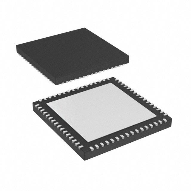
Package: 64-Pin VQFN (9 mm × 9 mm)
2 Applications
•
•
•
•
•
An input first-in first out block (FIFO) allows
independent data and sample clocks. FIFO input and
output pointers can be synchronized across multiple
devices for precise signal synchronization.
The DAC outputs are current sourcing and terminate
to GND with a compliance range of –0.5 V to +1 V.
The DAC3174 is pin compatible with the dualchannel, 500-MSPS, 12-bit DAC3164 and 10-bit
DAC3154, and the single-channel, 500-MSPS, 14-bit
DAC3171, 12-bit DAC3161, and 10-bit DAC3151.
The device is available in a 64-pin VQFN
PowerPAD™ package. and is specified over the full
industrial temperature range of –40°C to +85°C.
Device Information(1)
PART NUMBER
DAC3174
PACKAGE
VQFN (64)
BODY SIZE (NOM)
9.00 mm × 9.00 mm
(1) For all available packages, see the package option addendum
at the end of the data sheet.
Multi-Carrier, Multi-Mode Cellular Infrastructure
Base Stations
Radar
Signal Intelligence
Software-Defined Radios
Test and Measurement Instrumentation
Typical Application
DAC3174
Real
Mixer
Band-Pass
Filter
RF OUT
14-Bit DAC
800-MHz
Local Oscillator
DATA
FPGA
DATACLK
LVDS
Interface
FIFO
Real
Mixer
Band-Pass
Filter
RF OUT
14-Bit DAC
800-MHz
Local Oscillator
Data
Clock
Clock Distribution
DACCLK
CDCE62005
or
LMK048xx
Copyright © 2017, Texas Instruments Incorporated
1
An IMPORTANT NOTICE at the end of this data sheet addresses availability, warranty, changes, use in safety-critical applications,
intellectual property matters and other important disclaimers. PRODUCTION DATA.
�DAC3174
SLAS837B – APRIL 2013 – REVISED JANUARY 2017
www.ti.com
Table of Contents
1
2
3
4
5
6
Features ..................................................................
Applications ...........................................................
Description .............................................................
Revision History.....................................................
Pin Configuration and Functions .........................
Specifications.........................................................
6.1
6.2
6.3
6.4
6.5
6.6
6.7
6.8
6.9
7
1
1
1
2
3
7
Absolute Maximum Ratings ...................................... 7
ESD Ratings.............................................................. 7
Recommended Operating Conditions....................... 7
Thermal Information .................................................. 8
Electrical Characteristics: DC Specifications ............ 8
Electrical Characteristics: AC Specifications .......... 10
Electrical Characteristics: Digital Specifications ..... 10
Timing Requirements .............................................. 11
Typical Characteristics ............................................ 14
Detailed Description ............................................ 18
7.1 Overview ................................................................. 18
7.2 Functional Block Diagrams ..................................... 18
7.3 Feature Description................................................. 20
7.4 Device Functional Modes........................................ 21
7.5 Programming........................................................... 24
7.6 Register Maps ......................................................... 26
8
Application and Implementation ........................ 42
8.1 Application Information............................................ 42
8.2 Typical Application ................................................. 42
9 Power Supply Recommendations...................... 44
10 Layout................................................................... 45
10.1 Layout Guidelines ................................................. 45
10.2 Layout Example .................................................... 45
11 Device and Documentation Support ................. 46
11.1
11.2
11.3
11.4
11.5
11.6
Device Support......................................................
Receiving Notification of Documentation Updates
Community Resources..........................................
Trademarks ...........................................................
Electrostatic Discharge Caution ............................
Glossary ................................................................
46
46
46
47
47
47
12 Mechanical, Packaging, and Orderable
Information ........................................................... 47
4 Revision History
Changes from Revision A (May 2013) to Revision B
Page
•
Added Device Information, ESD Ratings, Recommended Operating Conditions, and Timing Requirements tables,
and Detailed Description, Application and Implementation, Power Supply Recommendations, Layout, Device and
Documentation Support, and Mechanical, Packaging, and Orderable Information sections ................................................. 1
•
Added typical application diagram to front page and moved existing block diagrams to Functional Block Diagrams
section .................................................................................................................................................................................... 1
•
Added GND PAD row to Pin Functions table ........................................................................................................................ 4
•
Added GND PAD row to Pin Functions table ........................................................................................................................ 6
•
Changed both functional block diagrams for clarity.............................................................................................................. 18
•
Added definition for T = DACCLK period ............................................................................................................................ 20
•
Added definition for T = DACCLK period ............................................................................................................................ 23
•
Changed text in FUSE controlled bullet of Register Maps section for clarity....................................................................... 26
Changes from Original (April 2013) to Revision A
•
2
Page
Deleted PRODUCT PREVIEW banner for device release ..................................................................................................... 1
Submit Documentation Feedback
Copyright © 2013–2017, Texas Instruments Incorporated
Product Folder Links: DAC3174
�DAC3174
www.ti.com
SLAS837B – APRIL 2013 – REVISED JANUARY 2017
5 Pin Configuration and Functions
VDDA18
NC
NC
IOUTAP
IOUTAN
VDDA33
EXTIO
BIASJ
VDDA33
VDDA33
IOUTBN
IOUTBP
NC
NC
VDDA18
SLEEP
64
63
62
61
60
59
58
57
56
55
54
53
52
51
50
49
RGC Package
64-Pin VQFN
Top View
DACCLKP
1
48
TXENABLE
DACCLKN
2
47
ALARM
CLKVDD18
3
46
SDO
ALIGNP
4
45
IOVDD
ALIGNN
5
44
SDIO
SYNCP
6
43
SCLK
SYNCN
7
42
SDENB
VFUSE
8
41
RESETB
DATA13P
9
40
DATA0N
DATA13N
10
39
DATA0P
DATA12P
11
38
DATA1N
DATA12N
12
37
DATA1P
DATA11P
13
36
DATA2N
DATA11N
14
35
DATA2P
DATA10P
15
34
DATA3N
DATA10N
16
33
DATA3P
17
18
19
20
21
22
23
24
25
26
27
28
29
30
31
32
DATA9P
DATA9N
DATA8P
DATA8N
DIGVDD18
DATA7P
DATA7N
DATACLKP
DATACLKN
DATA6P
DATA6N
DIGVDD18
DATA5P
DATA5N
DATA4P
DATA4N
GND PAD
Not to scale
Pin Functions: Single-Bus Mode
PIN
NAME
NO.
I/O
DESCRIPTION
CONTROL AND SERIAL
ALARM
47
O
CMOS output for ALARM condition.
RESETB
41
I
Serial interface reset input, active low. Initialized internal registers during high-to-low transition.
Asynchronous. Internal pullup. A reset event after every power cycle may be required to
reinitialize all SPI registers to default values.
SCLK
43
I
Serial interface clock. Internal pulldown.
SDENB
42
I
Serial data enable. Internal pullup.
SDIO
44
I/O
Bidirectional serial data in 3-pin mode (default). In 4-pin interface mode (sif4_ena [config0, bit 9]),
the SDIO pin in an input only. Internal pulldown.
Submit Documentation Feedback
Copyright © 2013–2017, Texas Instruments Incorporated
Product Folder Links: DAC3174
3
�DAC3174
SLAS837B – APRIL 2013 – REVISED JANUARY 2017
www.ti.com
Pin Functions: Single-Bus Mode (continued)
PIN
NAME
NO.
I/O
DESCRIPTION
SDO
46
O
Unidirectional serial interface data in 4-pin mode (sif4_ena [config0, bit 9]). The SDO pin is made
high impedance in 3-pin interface mode (default). Internal pulldown.
SLEEP
49
I
Puts device in sleep, active high. Internal pulldown.
TXENABLE
48
I
Transmit enable, active high input. TXENABLE must be high for the data to the DAC to be
enabled. When TXENABLE is low, the digital logic section is forced to all 0, and any input data
are ignored. Internal pulldown.
ALIGNN
5
I
ALIGNP
4
I
DATA[13:0]N
10, 12, 14,
16, 18, 20,
23, 27, 30,
32, 34, 36,
38, 40
I
DATA[13:0]P
9, 11, 13,
15, 17, 19,
22, 26, 29,
31, 33, 35,
37, 39
I
DATACLKN
25
I
DATACLKP
24
I
SYNCN
7
I
SYNCP
6
I
DACCLKN
2
I
DACCLKP
1
I
IOUTAN
60
O
IOUTAP
61
O
IOUTBN
54
O
IOUTBP
53
O
BIASJ
57
O
Full-scale output current bias. For 20-mA full-scale output current, connect a 960-Ω resistor to
GND.
EXTIO
58
I/O
Used as external reference input when internal reference is disabled. Requires a 0.1-µF
decoupling capacitor to GND when used as reference output.
CLKVDD18
3
I
1.8-V clock supply.
DIGVDD18
21, 28
I
1.8-V digital supply. Also supplies LVDS receivers.
DATA INTERFACE
LVPECL FIFO output synchronization. This positive or negative pair is captured with the rising
edge of DACCLKx. This pin is used to reset the clock dividers and for multiple DAC
synchronization. If unused, this pin can be left unconnected.
LVDS input data bits for both channels. Each positive and negative LVDS pair has an internal
100-Ω termination resistor. Data format relative to DATACLKx clock is dual data rate (DDR) with
two data transfers per DATACLKx clock cycles.
The data format is interleaved with channel A (rising edge) and channel B (falling edge).
In the default mode (reverse bus not enabled):
DATA13x is most significant data bit (MSB)
DATA0x is least significant data bit (LSB)
DDR differential input data clock. Edge to center nominal timing. Ch A rising edge, Ch B falling
edge in multiplexed output mode.
This pin resets the FIFO or is used as a syncing source. These two functions are captured with
the rising edge of DATACLKx. The signal captured by the falling edge of DATACLKx.
OUTPUT AND CLOCK
LVPECL clock input for DAC core with a self-bias of approximately CLKVDD18 / 2.
A-Channel DAC current output. An offset binary data pattern of 0x0000 at the DAC input results
in a full-scale current source, and the most positive voltage on the IOUTAP pin. Similarly, a
0xFFFF data input results in a 0-mA current source, and the least positive voltage on the
IOUTAP pin. The IOUTAN pin is the complement of IOUTAP.
B-Channel DAC current output. An offset binary data pattern of 0x0000 at the DAC input results
in a full-scale current source, and the most positive voltage on the IOUTBP pin. Similarly, a
0xFFFF data input results in a 0-mA current source, and the least positive voltage on the
IOUTBP pin. The IOUTBN pin is the complement of IOUTBP.
REFERENCE
POWER SUPPLY
IOVDD
45
I
Supply voltage for CMOS I/Os. 1.8 V to 3.3 V.
VDDA18
50, 64
I
Analog 1.8-V supply.
VDDA33
55, 56, 59
I
Analog 3.3-V supply.
VFUSE
8
I
Digital supply voltage (1.8 V). This supply pin is also used for factory fuse programming. Connect
to DVDD pins for normal operation.
51, 52,
62, 63
—
Not used. These pins can be left open or tied to ground in actual application use.
—
—
This thermal pad is the electrical ground connection for the device (backside).
NC
GND PAD
4
Submit Documentation Feedback
Copyright © 2013–2017, Texas Instruments Incorporated
Product Folder Links: DAC3174
�DAC3174
www.ti.com
SLAS837B – APRIL 2013 – REVISED JANUARY 2017
VDDA18
NC
NC
IOUTAP
IOUTAN
VDDA33
EXTIO
BIASJ
VDDA33
VDDA33
IOUTBN
IOUTBP
NC
NC
VDDA18
SLEEP
64
63
62
61
60
59
58
57
56
55
54
53
52
51
50
49
RGC Package
64-Pin VQFN
Top View
DACCLKP
1
48
TXENABLE
DACCLKN
2
47
ALARM
CLKVDD18
3
46
SDO
NC
4
45
IOVDD
NC
5
44
SDIO
DA_CLKP
6
43
SCLK
DA_CLKN
7
42
SDENB
VFUSE
8
41
RESETB
DA6P
9
40
DB0N
DA6N
10
39
DB0P
DA5P
11
38
DB1N
DA5N
12
37
DB1P
DA4P
13
36
DB2N
DA4N
14
35
DB2P
DA3P
15
34
DB3N
DA3N
16
33
DB3P
17
18
19
20
21
22
23
24
25
26
27
28
29
30
31
32
DA2P
DA2N
DA1P
DA1N
DIGVDD18
DA0P
DA0N
DB_CLKP
DB_CLKN
DB6P
DB6N
DIGVDD18
DB5P
DB5N
DB4P
DB4N
GND PAD
Not to scale
Pin Functions: Dual-Bus Mode
PIN
NAME
NO.
I/O
DESCRIPTION
CONTROL AND SERIAL
ALARM
47
O
CMOS output for alarm condition.
RESETB
41
I
Serial interface reset input, active low. Initializes internal registers during high to low transition.
Asynchronous. Internal pullup. A reset event after every power cycle may be required to
reinitialize all SPI registers to default values.
SCLK
43
I
Serial interface clock. Internal pulldown.
SDENB
42
I
Serial data enable. Internal pullup.
SDIO
44
I/O
Bidirectional serial data in 3-pin mode (default). In 4-pin interface mode (sif4_ena [config0, bit 9]),
the SDIO pin in an input only. Internal pulldown.
Submit Documentation Feedback
Copyright © 2013–2017, Texas Instruments Incorporated
Product Folder Links: DAC3174
5
�DAC3174
SLAS837B – APRIL 2013 – REVISED JANUARY 2017
www.ti.com
Pin Functions: Dual-Bus Mode (continued)
PIN
NAME
NO.
I/O
DESCRIPTION
SDO
46
O
Unidirectional serial interface data in 4-pin mode (sif4_ena [config0, bit 9]). The SDO pin is made
high impedance in 3-pin interface mode (default). Internal pulldown.
SLEEP
49
I
Puts device in sleep, active high. Internal pulldown.
TXENABLE
48
I
Transmit enable, active high input. TXENABLE must be high for the data to the DAC to be
enabled. When TXENABLE is low, the digital logic section is forced to all 0, and any input data
are ignored. Internal pulldown.
DA[6:0]N
10, 12, 14,
16, 18
I
DA[6:0]P
9, 11, 13,
15, 17, 19
I
DB[6:0]N
27, 30, 32,
34, 36, 38,
40
I
DB[6:0]P
26, 29, 31,
33, 35, 37,
39
I
DA_CLKN
7
I
DA_CLKP
6
I
DB_CLKN
25
I
DB_CLKP
24
I
DACCLKN
2
I
LVPECL clock negative input for DAC core with a self-bias of approximately CLKVDD18 / 2.
DACCLKP
1
I
LVPECL clock positive input for DAC core with a self-bias of approximately CLKVDD18 / 2.
IOUTAN
60
O
IOUTAP
61
O
A-Channel DAC current output. An offset binary data pattern of 0x0000 at the DAC input results
in a full-scale current source, and the most positive voltage on the IOUTAP pin. Similarly, a
0xFFFF data input results in a 0-mA current source, and the least positive voltage on the
IOUTAP pin. The IOUTAN pin is the complement of IOUTAP.
IOUTBN
54
O
IOUTBP
53
O
BIASJ
57
O
Full-scale output current bias. For 20-mA full-scale output current, connect a 960-Ω resistor to
GND.
EXTIO
58
I/O
Used as external reference input when internal reference is disabled. Requires a 0.1-µF
decoupling capacitor to GND when used as reference output.
CLKVDD18
3
I
1.8-V clock supply.
DIGVDD18
21, 28
I
1.8-V digital supply. Also supplies LVDS receivers.
45
I
Supply voltage for CMOS I/Os. 1.8 V to 3.3 V.
VDDA18
50, 64
I
Analog 1.8-V supply.
VDDA33
55, 56, 59
I
Analog 3.3-V supply.
VFUSE
8
I
Digital supply voltage (1.8 V). This supply pin is also used for factory fuse programming. Connect
to DVDD pins for normal operation.
4, 5,
51, 52,
62, 63
—
Not used. In actual application, pins 51, 52, 62, and 63 can be left open or tied to ground. TI
recommends tying pins 4 and 5 to DIGVDD18 and ground, respectively.
—
—
This thermal pad is the electrical ground connection for the device (backside).
DATA INTERFACE
LVDS positive input data bits for channel A. Each positive or negative LVDS pair has an internal
100-Ω termination resistor. Data format relative to DA_CLKx clock is dual data rate (DDR) with
two data transfers per DA_CLKx clock cycle.
The data format is 7 MSBs (rising edge) and 7 LSBs (falling edge).
In the default mode (reverse bus not enabled):
DA6x is most significant data bit (MSB)
DA0x is least significant data bit (LSB)
LVDS positive input data bits for channel B. Each positive or negative LVDS pair has an internal
100-Ω termination resistor. Data format relative to DB_CLKx clock is dual data rate (DDR) with
two data transfers per DB_CLKx clock cycle.
The data format is 7 MSBs (rising edge) and 7 LSBs (falling edge).
In the default mode (reverse bus not enabled):
DB6x is most significant data bit (MSB)
DB0x is least significant data bit (LSB)
DDR differential input data clock for channel A. Edge to center nominal timing.
DDR differential input data clock for channel B. Edge to center nominal timing.
OUTPUT AND CLOCK
B-Channel DAC current output. An offset binary data pattern of 0x0000 at the DAC input results
in a full-scale current source, and the most positive voltage on the IOUTBP pin. Similarly, a
0xFFFF data input results in a 0-mA current source, and the least positive voltage on the
IOUTBP pin. The IOUTBN pin is the complement of IOUTBP.
REFERENCE
POWER SUPPLY
IOVDD
NC
GND PAD
6
Submit Documentation Feedback
Copyright © 2013–2017, Texas Instruments Incorporated
Product Folder Links: DAC3174
�DAC3174
www.ti.com
SLAS837B – APRIL 2013 – REVISED JANUARY 2017
6 Specifications
6.1 Absolute Maximum Ratings
over operating free-air temperature range (unless otherwise noted) (1)
Supply voltage
Terminal voltage
Temperature
MIN
MAX
VDDA33 to GND
–0.5
4
VDDA18 to GND
–0.5
2.3
CLKVDD18 to GND
–0.5
2.3
IOVDD to GND
–0.5
4
DIGVDD18 to GND
–0.5
2.3
CLKVDD18 to DIGVDD18
–0.5
0.5
VDDA18 to DIGVDD18
–0.5
0.5
DA[6:0]P, DA[6:0]N, DB[6:0]P, DB[6:0]N, D[13:0]P, D[13:0]N,
DATACLKP, DATACLKN, DA_CLKP, DA_CLKPN, DB_CLKP,
DB_CLKN, SYNCP, SYNCN to GND
–0.5
DIGVDD18 + 0.5
DACCLKP, DACCLKN, ALIGNP, ALIGNN
–0.5
CLKVDD18 + 0.5
TXENABLE, ALARM, SDO, SDIO, SCLK, SDENB, RESETB to GND
–0.5
IOVDD + 0.5
IOUTAP, IOUTAN, IOUTBP, IOUTBN to GND
–0.7
1.4
EXTIO, BIASJ to GND
–0.5
VDDA33 + 0.5
Operating ambient free-air, TA
–40
V
V
85
Maximum junction, TJ
125
Storage, Tstg
(1)
UNIT
–65
°C
150
Stresses beyond those listed under Absolute Maximum Ratings may cause permanent damage to the device. These are stress ratings
only, which do not imply functional operation of the device at these or any other conditions beyond those indicated under Recommended
Operating Conditions. Exposure to absolute-maximum-rated conditions for extended periods may affect device reliability.
6.2 ESD Ratings
VALUE
V(ESD)
(1)
(2)
Electrostatic discharge
Human-body model (HBM), per ANSI/ESDA/JEDEC JS-001 (1)
±2000
Charged-device model (CDM), per JEDEC specification JESD22-C101 (2)
±500
UNIT
V
JEDEC document JEP155 states that 500-V HBM allows safe manufacturing with a standard ESD control process.
JEDEC document JEP157 states that 250-V CDM allows safe manufacturing with a standard ESD control process.
6.3 Recommended Operating Conditions
MIN
NOM
MAX
UNIT
CLKVDD18
Clock buffer supply
1.71
1.8
1.89
V
DIGVDD18
Digital supply
1.71
1.8
1.89
V
VDDA18
1.8-V analog supply
1.71
1.8
1.89
V
VFUSE
Fuse bank supply
1.71
1.8
1.89
V
IOVDD
IO supply (1)
1.71
3.45
V
VDDA33
3.3-V analog supply
3.15
3.3
3.45
V
TA
Operating ambient free-air temperature
–40
25
85
°C
TJ
Operating junction temperature (2)
105
°C
(1)
(2)
Sets CMOS IO voltage levels; nominal 1.8 V, 2.5 V, or 3.3 V.
Prolonged use at this junction temperature may increase the device failure-in-time (FIT) rate.
Submit Documentation Feedback
Copyright © 2013–2017, Texas Instruments Incorporated
Product Folder Links: DAC3174
7
�DAC3174
SLAS837B – APRIL 2013 – REVISED JANUARY 2017
www.ti.com
6.4 Thermal Information
DAC3174
THERMAL METRIC (1)
RGC (VQFN)
UNIT
64 PINS
RθJA
Junction-to-ambient thermal resistance
23
°C/W
RθJC(top)
Junction-to-case (top) thermal resistance
7.6
°C/W
RθJB
Junction-to-board thermal resistance
2.8
°C/W
ψJT
Junction-to-top characterization parameter
0.1
°C/W
ψJB
Junction-to-board characterization parameter
2.8
°C/W
RθJC(bot)
Junction-to-case (bottom) thermal resistance
0.2
°C/W
(1)
For more information about traditional and new thermal metrics, see the Semiconductor and IC Package Thermal Metrics application
report.
6.5 Electrical Characteristics: DC Specifications
Typical values at TA = 25°C, full temperature range is TMIN = –40°C to TMAX = 85°C, DAC sample rate = 500 MSPS, 50%
clock duty cycle, VDDA33 = IOVDD = 3.3 V, VDDA18 = CLKVDD18 = DIGVDD18 = 1.8 V, and IOUTFS = 20 mA (unless
otherwise noted).
PARAMETER
TEST CONDITIONS
Resolution
MIN
TYP
MAX
14
UNIT
Bits
DC ACCURACY
DNL
INL
Differential nonlinearity
Integral nonlinearity
1 LSB = IOUTFS / 214
±1
LSB
14
±2
LSB
±0.4
LSB
0.01
%FSR
1 LSB = IOUTFS / 2
ANALOG OUTPUTS
Coarse gain linearity
Offset error
Gain error
Midcode offset
With external reference
±2
With internal reference
±2
–2
%FSR
Gain mismatch
With internal reference
Minimum full-scale output current
Nominal full-scale current,
IOUTFS = 16 × IBAIS current
2
2
mA
Maximum full-scale output current
Nominal full-scale current,
IOUTFS = 16 × IBAIS current
20
mA
Output compliance
IOUTFS = 20 mA
–0.5
Output resistance
Output capacitance
1
%FSR
V
300
kΩ
5
pF
REFERENCE OUTPUT
VREF
Reference output voltage
1.14
Reference output current
1.2
1.26
100
V
nA
REFERENCE INPUT
VEXTIO input voltage
External reference mode
Input resistance
0.1
1.2
1.25
V
1
MΩ
Small-signal bandwidth
500
kHz
Input capacitance
100
pF
±1
ppm of
FSR/°C
TEMPERATURE COEFFICIENTS
Offset drift
Gain drift
8
With external reference
±15
With internal reference
±30
Reference voltage drift
±8
Submit Documentation Feedback
Copyright © 2013–2017, Texas Instruments Incorporated
Product Folder Links: DAC3174
ppm /°C
�DAC3174
www.ti.com
SLAS837B – APRIL 2013 – REVISED JANUARY 2017
Electrical Characteristics: DC Specifications (continued)
Typical values at TA = 25°C, full temperature range is TMIN = –40°C to TMAX = 85°C, DAC sample rate = 500 MSPS, 50%
clock duty cycle, VDDA33 = IOVDD = 3.3 V, VDDA18 = CLKVDD18 = DIGVDD18 = 1.8 V, and IOUTFS = 20 mA (unless
otherwise noted).
PARAMETER
TEST CONDITIONS
MIN
TYP
MAX
MODE 1, fDAC = 491.52 MSPS, QMC on,
IF = 20 MHz
52
59
MODE 2, fDAC = 320 MSPS, QMC on,
IF = 20 MHz
51
MODE 3, sleep mode, fDAC = 491.52
MSPS, DAC in sleep mode
2.6
MODE 4, power-down mode, no clock,
DAC in sleep mode
1.6
4
MODE 1, fDAC = 491.52 MSPS, QMC on,
IF = 20 MHz
49
57
MODE 2, fDAC = 320 MSPS, QMC on,
IF = 20 MHz
38
MODE 3, sleep mode, fDAC = 491.52
MSPS, DAC in sleep mode
43
MODE 4, power-down mode, no clock,
DAC in sleep mode
1.8
4
MODE 1, fDAC = 491.52 MSPS, QMC on,
IF = 20 MHz
115
130
UNIT
POWER CONSUMPTION
IVDDA33
ICLKVDD18
IDIGVDD18
IIOVDD
Pdis
3.3-V analog supply current
1.8-V clock and analog supply current
(CLKVDD18 and VDDA18)
1.8-V digital supply current
(DIGVDD18 and VFUSE)
1.8-V IO supply current
Total power dissipation
mA
mA
MODE 2, fDAC = 320 MSPS, QMC on,
IF = 20 MHz
87
MODE 3, sleep mode, fDAC = 491.52
MSPS, DAC in sleep mode
110
MODE 4, power-down mode, no clock,
DAC in sleep mode
0.7
3
MODE 1, fDAC = 491.52 MSPS, QMC on,
IF = 20 MHz
0.002
0.015
MODE 2, fDAC = 320 MSPS, QMC on,
IF = 20 MHz
0.002
MODE 3, sleep mode, fDAC = 491.52
MSPS, DAC in sleep mode
0.003
MODE 4, power-down mode, no clock,
DAC in sleep mode
0.003
0.015
MODE 1, fDAC = 491.52 MSPS, QMC on,
IF = 20 MHz
464
530
MODE 2, fDAC = 320 MSPS, QMC on,
IF = 20 MHz
396
MODE 3, sleep mode, fDAC = 491.52
MSPS, DAC in sleep mode
284
mA
mA
mW
MODE 4, power-down mode, no clock,
DAC in sleep mode
PSRR
Power-supply rejection ratio
DC tested
10
–0.4
26
0.4
%FSR/V
Submit Documentation Feedback
Copyright © 2013–2017, Texas Instruments Incorporated
Product Folder Links: DAC3174
9
�DAC3174
SLAS837B – APRIL 2013 – REVISED JANUARY 2017
www.ti.com
6.6 Electrical Characteristics: AC Specifications
Typical values at T A = 25°C, full temperature range is TMIN = –40°C to TMAX = 85°C, DAC sample rate = 500 MSPS, 50%
clock duty cycle, VDDA33 = IOVDD = 3.3 V, VDDA18 = CLKVDD18 = DIGVDD18 = 1.8 V, and IOUT FS = 20 mA (unless
otherwise noted).
PARAMETER
TEST CONDITIONS
MIN
TYP MAX
UNIT
ANALOG OUTPUT
fDAC
Maximum sample rate
500
ts(DAC)
Output settling time to 0.1%
Transition: Code 0x0000 to 0x3FFF
tPD
Output propagation delay
Does not include digital latency
tr(IOUT)
Output rise time
tf(IOUT)
MSPS
11
ns
2
ns
10% to 90%
200
ps
Output fall time
90% to 10%
200
ps
Digital latency
Length of delay from DAC pin inputs to DATA at output
pins. In normal operation mode including the latency of
FIFO.
26
DACCLK
fDAC = 500 MSPS, fout = 10.1 MHz
82
fDAC = 500 MSPS, fout = 20.1 MHz
78
fDAC = 500 MSPS, fout = 70.1 MHz
74
fDAC = 500 MSPS, fout = 10.1 ±0.5 MHz
84
fDAC = 500 MSPS, fout = 20.1 ±0.5 MHz
84
fDAC = 500 MSPS, fout = 70.1 ±0.5 MHz
75
AC PERFORMANCE
SFDR
IMD3
Spurious free dynamic
Intermodulation distortion
fDAC = 500 MSPS, fout = 150.1 ±0.5 MHz
NSD
ACLR
Noise spectral density
Adjacent channel leakage ratio
dBc
dBc
63
fDAC = 500 MSPS, fout = 10.1 MHz
160
fDAC = 500 MSPS, fout = 20.1 MHz
157
fDAC = 500 MSPS, fout = 70.1 MHz
155
fDAC = 491.52 MSPS, fout = 30.72 MHz, WCDMA TM1
78
f AC = 491.52 MSPS, fout = 153.6 MHz, WCDMA TM1
74
dBc/Hz
dBc
6.7 Electrical Characteristics: Digital Specifications
Typical values at T A = 25°C, full temperature range is T MIN = –40°C to T MAX = 85°C, DAC sample rate = 500 MSPS, 50%
clock duty cycle, VDDA33 = IOVDD = 3.3 V, VDDA18 = CLKVDD18 = DIGVDD18 = 1.8 V, and IOUT FS = 20 mA (unless
otherwise noted).
PARAMETERS
TEST CONDITIONS
MIN
TYP
MAX
UNIT
CMOS DIGITAL INPUTS (RESETB, SDENB, SCLK, SDIO, TXENABLE)
VIH
High-level input voltage
IOVDD = 3.3 V, 2.5 V, or 1.8 V
VIL
Low-level input voltage
IOVDD = 3.3 V, 2.5 V, or 1.8 V
IIH
High-level input current
IOVDD = 3.3 V, 2.5 V, or 1.8 V
IIL
Low-level input current
IOVDD = 3.3 V, 2.5 V, or 1.8 V
IOVDD × 0.6
V
0.25 × IOVDD
V
–40
40
µA
–40
40
µA
DIGITAL OUTPUTS – CMOS INTERFACE (SDOUT, SDIO)
VOH
High-level output voltage
VOL
Low-level output voltage
IOVDD = 3.3 V, 2.5 V, or 1.8 V
0.85 × IOVDD
V
0.125 × IOVDD
V
LVPECL INPUTS – (DACCLKx, ALIGNx)
VCM
LVPECL input common-mode voltage
VIDIFF
Differential input peak-to-peak voltage
10
0.4
Submit Documentation Feedback
0.5
V
1
V
Copyright © 2013–2017, Texas Instruments Incorporated
Product Folder Links: DAC3174
�DAC3174
www.ti.com
SLAS837B – APRIL 2013 – REVISED JANUARY 2017
Electrical Characteristics: Digital Specifications (continued)
Typical values at T A = 25°C, full temperature range is T MIN = –40°C to T MAX = 85°C, DAC sample rate = 500 MSPS, 50%
clock duty cycle, VDDA33 = IOVDD = 3.3 V, VDDA18 = CLKVDD18 = DIGVDD18 = 1.8 V, and IOUT FS = 20 mA (unless
otherwise noted).
PARAMETERS
TEST CONDITIONS
MIN
TYP
MAX
UNIT
LVDS INTERFACE (DATA[13:0]x, DA[6:0]x , DB[6:0]x , DA_CLKx, DB_CLKx, DATACLKx, SYNCx)
VA,B+
Logic high differential input voltage
threshold
VA,B–
Logic low differential input voltage
threshold
VCOM
LVDS input common-mode voltage
ZT
Internal termination
CL
LVDS input capacitance
175
mV
–175
mV
1
1.2
2
V
85
110
135
Ω
2
pF
6.8 Timing Requirements
Typical values at T A = 25°C, full temperature range is T MIN = –40°C to T MAX = 85°C, DAC sample rate = 500 MSPS, 50%
clock duty cycle, VDDA33 = IOVDD = 3.3 V, VDDA18 = CLKVDD18 = DIGVDD18 = 1.8 V, and IOUT FS = 20 mA (unless
otherwise noted).
MIN
TYP
MAX
UNIT
SERIAL PORT TIMING
ts(SENDB)
Setup time, SDENB to rising edge of SCLK
20
ns
ts(SDIO)
Setup time, SDIO to rising edge of SCLK
10
ns
th(SDIO)
Hold time, SDIO from rising edge of SCLK
5
ns
t(SCLK)
Period of SCLK
100
ns
t(SCLKH)
High time of SCLK
40
ns
t(SCLKL)
Low time of SCLK
40
ns
td(DATA)
Data output delay after falling edge of SCLK
10
ns
TRESET
Minimum RESTB pulse duration
25
ns
LVDS INPUT TIMING
config3 Setting
ts(DATA)
Setup time
D[x..0] valid to DATACLK rising or falling edge
for single bus single clock mode ;
DA/DB[x…0] valid to DB_CLK rising or falling
edge for dual bus single clock mode;
DA[x..0] valid to DA_CLK rising or falling edge,
and DB[x…0] valid for DB_CLK rising or falling
edge for dual bus dual clock mode
datadly
clkdly
0
0
–20
0
1
–120
0
2
–220
0
3
–310
0
4
–390
0
5
–480
0
6
–560
0
7
–630
1
0
70
2
0
150
3
0
230
4
0
330
5
0
430
6
0
530
7
0
620
Submit Documentation Feedback
Copyright © 2013–2017, Texas Instruments Incorporated
Product Folder Links: DAC3174
ps
11
�DAC3174
SLAS837B – APRIL 2013 – REVISED JANUARY 2017
www.ti.com
Timing Requirements (continued)
Typical values at T A = 25°C, full temperature range is T MIN = –40°C to T MAX = 85°C, DAC sample rate = 500 MSPS, 50%
clock duty cycle, VDDA33 = IOVDD = 3.3 V, VDDA18 = CLKVDD18 = DIGVDD18 = 1.8 V, and IOUT FS = 20 mA (unless
otherwise noted).
MIN
TYP
MAX
UNIT
config3 Setting
th(DATA)
Hold time
D[x..0] valid to DATACLK rising or falling edge
for single bus single clock mode;
DA/DB[x…0] valid to DB_CLK rising or falling
edge for dual bus single clock mode;
DA[x..0] valid to DA_CLK rising or falling edge,
and DB[x…0] valid for DB_CLK rising or falling
edge for dual bus dual clock mode.
D[13:0]P/N
datadly
clkdly
0
0
310
0
1
390
0
2
480
0
3
560
0
4
650
0
5
740
0
6
850
0
7
930
1
0
200
2
0
100
3
0
20
4
0
–60
5
0
–140
6
0
–220
7
0
–290
ps
A3[13:0] B3[13:0] A4[13:0] B4[13:0] A5[13:0] B5[13:0] A6[13:0] B6[13:0] A7[13:0] B7[13:0]
t s(DATA )
t h(DATA )
t s(DATA )
t h(DATA )
t s(DATA )
t h(DATA )
DATACLKP/N
(DDR)
SYNCP/N
Resets write pointer to position 0
Figure 1. Input Data Timing for Single-Bus, Single-Clock Mode
12
Submit Documentation Feedback
Copyright © 2013–2017, Texas Instruments Incorporated
Product Folder Links: DAC3174
�DAC3174
www.ti.com
SLAS837B – APRIL 2013 – REVISED JANUARY 2017
DA[6:0]P/N
A3[13:7]
A4[13:7]
A3[6:0]
t s(DATA )
A4[6:0]
A5[13:7]
t h(DATA )
A5[6:0]
A6[13:7]
A6[6:0]
A7[13:7]
A7[6:0]
t h(DATA )
t s(DATA )
DA_CLKP/N
There is no phase relationship requirement
between DA_CLK and DB_CLK
DB[6:0]P/N
B3[13:7]
B3[6:0]
B4[13:7]
t s(DATA )
B4[6:0]
B5[13:7]
t h(DATA )
B5[6:0]
t s(DATA )
B6[13:7]
B6[6:0]
B7[13:7]
B7[6:0]
t h(DATA )
DB_CLKP/N
Figure 2. Input Data Timing for Dual-Bus, Dual-Clock Mode
DA[6:0]P/N
A3[13:7]
A3[6:0]
A4[13:7]
t s(DATA
(
)
DB[6:0]P/N
B3[13:7]
B3[6:0]
A4[6:0]
t h(DATA )
B4[13:7]
t s(DATA )
B4[6:0]
t h(DATA )
A5[13:7]
A5[6:0]
t s(DATA
(
)
B5[13:7]
t s(DATA )
A6[13:7]
A6[6:0]
A7[13:7]
A7[6:0]
B6[6:0]
B7[13:7]
B7[6:0]
t h(DATA )
B5[6:0]
B6[13:7]
t h(DATA )
DB_CLKP/N
Figure 3. Input Data Timing for Dual-Bus, Single-Clock Mode
D[13:0]P/N
A3[13:0] A4[13:0] A5[13:0] A6[13:0] A7[13:0] A8[13:0] A9[13:0] A10[13:0] A11 [13:0]
t s(DATA
(
)
t h(DATA )
t s(DATA )
t h(DATA )
DATACLKP/N
(SDR)
SYNCP/N
Resets write pointer to position 0
Figure 4. Input Data Timing for Single-Channel, Single Data Rate (SDR) Mode
Submit Documentation Feedback
Copyright © 2013–2017, Texas Instruments Incorporated
Product Folder Links: DAC3174
13
�DAC3174
SLAS837B – APRIL 2013 – REVISED JANUARY 2017
www.ti.com
6.9 Typical Characteristics
All plots are at 25°C, nominal supply voltages, fDAC = 500 MSPS, 50% clock duty cycle, 0-dBFS input signal, and 20-mA fullscale output current (unless otherwise noted).
2
Differential Nonlinearity Error (LSB)
Integral Nonlinearity Error (LSB)
2
1.5
1
0.5
0
−0.5
−1
−1.5
−2
5000
10000
1
0.5
0
−0.5
−1
−1.5
−2
15000
Code
1.5
5000
10000
15000
Code
G019
G020
Figure 5. Integral Nonlinearity
Figure 6. Differential Nonlinearity
Figure 7. SFDR vs Output Frequency Over Input Scale
Figure 8. Second-Order Harmonic Distortion
vs Output Frequency Over Input Scale
100
fDAC = 200 MSPS
fDAC = 300 MSPS
fDAC = 400 MSPS
fDAC = 500 MSPS
90
SFDR (dBc)
80
70
60
50
40
30
20
Figure 9. Third-Order Harmonic Distortion
vs Output Frequency Over Input Scale
14
0
50
100
150
Output Frequency (MHz)
200
250
G004
Figure 10. SFDR vs Output Frequency Over fDAC
Submit Documentation Feedback
Copyright © 2013–2017, Texas Instruments Incorporated
Product Folder Links: DAC3174
�DAC3174
www.ti.com
SLAS837B – APRIL 2013 – REVISED JANUARY 2017
Typical Characteristics (continued)
All plots are at 25°C, nominal supply voltages, fDAC = 500 MSPS, 50% clock duty cycle, 0-dBFS input signal, and 20-mA fullscale output current (unless otherwise noted).
100
fDAC = 200 MSPS
fDAC = 300 MSPS
fDAC = 400 MSPS
fDAC = 500 MSPS
90
80
IMD3 (dBc)
70
60
50
40
30
20
0
Figure 11. IMD3 vs Output Frequency Over Input Scale
50
100
150
Output Frequency (MHz)
200
250
G006
Figure 12. IMD3 vs Output Frequency Over fDAC
180
fDAC = 200 MSPS
fDAC = 300 MSPS
fDAC = 400 MSPS
fDAC = 500 MSPS
170
NSD (dBc/Hz)
160
150
140
130
120
110
0
Figure 13. NSD vs Output Frequency Over Input Scale
100
Output Frequency (MHz)
G008
−50
Adjacent channel
Altenate channel
−60
ACLR (dBc)
−60
ACLR (dBc)
250
Figure 14. NSD vs Output Frequency Over fDAC
−50
−70
−80
−90
−70
−80
−90
fDAC = 500 MSPS
−100
200
0
50
100
150
Output Frequency (MHz)
fDAC = 500 MSPS
200
250
−100
0
G009
Figure 15. ACLR (Adjacent Channel) vs Output Frequency
50
100
150
Output Frequency (MHz)
200
250
G010
Figure 16. ACLR (Alternate Channel) vs Output Frequency
Submit Documentation Feedback
Copyright © 2013–2017, Texas Instruments Incorporated
Product Folder Links: DAC3174
15
�DAC3174
SLAS837B – APRIL 2013 – REVISED JANUARY 2017
www.ti.com
Typical Characteristics (continued)
All plots are at 25°C, nominal supply voltages, fDAC = 500 MSPS, 50% clock duty cycle, 0-dBFS input signal, and 20-mA fullscale output current (unless otherwise noted).
10
10
fDAC= 491.52 MSPS
fOUT = 20 MHz
−10
−10
−20
−20
−30
−40
−50
−30
−40
−50
−60
−60
−70
−70
−80
−80
−90
10
50
90
130
170
Frequency (MHz)
210
fDAC= 491.52 MSPS
fOUT = 20 MHz
0
Power (dBm)
Power (dBm)
0
−90
250
10
50
90
G011
IF = 20 MHz
Figure 17. Single-Tone Spectral Plot
250
G012
Figure 18. Single-Tone Spectral Plot
10
fDAC = 500 MSPS
fout = 20 MHz
Tone spacing = 1 MHz
0
−10
fDAC = 500 MSPS
fout = 70 MHz
Tone spacing = 1 MHz
0
−10
−20
Power (dBm)
−20
Power (dBm)
210
IF = 70 MHz
10
−30
−40
−50
−60
−30
−40
−50
−60
−70
−70
−80
−80
−90
−90
−100
−100
15
17
19
21
Frequency (MHz)
23
25
65
67
G013
IF = 20 MHz
69
71
Frequency (MHz)
73
75
G014
IF = 70 MHz
Figure 19. Two-Tone Spectral Plot
0dBFs,
fDAC = 491.52MSPS,
fOUT = 70MHz
Figure 20. Two-Tone Spectral Plot
0dBFs,
fDAC = 491.52MSPS,
fOUT = 70MHz
Figure 21. Four-Carrier WCDMA Test Mode 1
16
130
170
Frequency (MHz)
Figure 22. Single-Carrier WCDMA Test Mode 1
Submit Documentation Feedback
Copyright © 2013–2017, Texas Instruments Incorporated
Product Folder Links: DAC3174
�DAC3174
www.ti.com
SLAS837B – APRIL 2013 – REVISED JANUARY 2017
Typical Characteristics (continued)
All plots are at 25°C, nominal supply voltages, fDAC = 500 MSPS, 50% clock duty cycle, 0-dBFS input signal, and 20-mA fullscale output current (unless otherwise noted).
Ref -20 dBm
-30
-40
*Att 5 dB
*RBW 30 kHz
*VBW 300 kHz
*SWT 2 s
Ref -20 dBm
-30
0dBFs,
fDAC = 491.52MSPS,
fOUT = 70MHz
A
-40
-50
1 RM *
CLRWR -60
-50
1 RM *
CLRWR -60
-70
-70
*Att 5 dB
*RBW 30 kHz
*VBW 300 kHz
*SWT 2 s
0dBFs,
fDAC = 491.52MSPS,
fOUT = 70MHz
A
-80
-80
NOR
-90
NOR
-90
-100
-100
3DB
-110
Center 70 MHz
Tx Channel
Bandwidth
Adjacent Channel
Bandwidth
Spacing
2.92827419 MHz/
Span 29.2827419 MHz
E-UTRA/LTE Square
9.015 MHz
Power
-12.31 dBm
9.015 MHz
10 MHz
Lower
Upper
-74.95 dB
-74.23 dB
Figure 23. ACPR – LTE 10-MHz FDD E-TM 1.1
3DB
-110
Center 70 MHz
Tx Channel
Bandwidth
5.855034538 MHz/
Span 58.55034538 MHz
E-UTRA/LTE Square
18.015 MHz
Power
-11.16 dBm
Adjacent Channel
Bandwidth
Spacing
Lower
-72.43 dB
18.015 MHz
20 MHz
Upper
-72.21 dB
Figure 24. ACPR – LTE 20-MHz FDD E-TM 1.1
Submit Documentation Feedback
Copyright © 2013–2017, Texas Instruments Incorporated
Product Folder Links: DAC3174
17
�DAC3174
SLAS837B – APRIL 2013 – REVISED JANUARY 2017
www.ti.com
7 Detailed Description
7.1 Overview
The DAC3174 device is a dual-channel, 14-bit, 500-MSPS, digital-to-analog converter (DAC), and uses a 14-bit,
wide LVDS digital bus with an input FIFO. The data for the two channels are multiplexed onto the 14-bit LVDS
bus in a dual-data-rate (DDR) fashion. The DAC3174 also supports a DDR, 7-bit, LVDS interface mode for each
channel.
The DAC3174 has separate input data clock for the digital data and sample clock for the analog output. The
FIFO input and output pointers can be synchronized across multiple devices for precise signal synchronization.
The DAC outputs are current sourcing and terminate to GND with a compliance range of –0.5 V to +1 V. The
DAC3174 is pin-compatible with the 12-bit DAC3164 and 10-bit DAC3154. as well as the single-channel
DAC31x1 family.
VDDA18
VFUSE
DIGVDD18
CLKVDD18
7.2 Functional Block Diagrams
DACCLKP
LVPECL
1. 2- V
Reference
Clock Distribution
DACCLKN
DATACLKN
Programmable
Delay
LVDS
DACA
Gain
QMC
A-Offset
100
DATA13P
BIASJ
LVDS
100
DATACLKP
EXTIO
DATA13N
IOUTBP
14-Bit
DACB
14
IOUTBN
100
LVDS
QMC
B-Offset
DATA0N
DACB
Gain
LVDS
VDDA33
100
SYNCP
IOUTAN
8-Sample FIFO
Deinterleave
Pattern Test
14
DATA0P
IOUTAP
14-Bit
DACA
SYNCN
Optional Input
ALIGNP
Used for Multi-DAC Sync
Control Interface
LVPECL
TESTMODE
ALARM
SLEEP
RESETB
TXENABLE
SCLK
SDENB
SDIO
SDO
IOVDD
GND
ALIGNN
Figure 25. 14-Bit Interface Mode
18
Submit Documentation Feedback
Copyright © 2013–2017, Texas Instruments Incorporated
Product Folder Links: DAC3174
�DAC3174
www.ti.com
SLAS837B – APRIL 2013 – REVISED JANUARY 2017
VDDA18
VFUSE
DIGVDD18
CLKVDD18
Functional Block Diagrams (continued)
DACCLKP
LVPECL
1. 2- V
Reference
Clock Distribution
DACCLKN
DA_CLKN
LVDS
DACA
Gain
QMC
A-Offset
8-Sample FIFO
14-Bit
DACA
8-Sample FIFO
14
100
Deinterleave
Pattern Test
DA6N
DA0P
Programmable
Delay
100
DA6P
BIASJ
LVDS
100
DA_CLKP
EXTIO
14-Bit
DACB
IOUTAP
IOUTAN
DA0N
LVDS
100
DB_CLKN
LVDS
100
DB6P
Pattern Test
DB6N
14
100
DB0P
Programmable
Delay
Deinterleave
DB_CLKP
QMC
B-Offset
DB0N
IOUTBP
IOUTBN
DACB
Gain
VDDA33
TESTMODE
ALARM
SLEEP
RESETB
TXENABLE
SCLK
SDENB
SDIO
SDO
GND
IOVDD
Control Interface
Figure 26. 7-Bit Interface Mode
Submit Documentation Feedback
Copyright © 2013–2017, Texas Instruments Incorporated
Product Folder Links: DAC3174
19
�DAC3174
SLAS837B – APRIL 2013 – REVISED JANUARY 2017
www.ti.com
7.3 Feature Description
7.3.1 Alarm Monitoring
The DAC3174 includes flexible alarm monitoring that can be used to alert a possible malfunction scenario. All
alarm events can be accessed either through the SIP registers and through the ALARM pin. After an alarm is set,
the corresponding alarm bit in register config5 must be reset through the serial interface in order to allow further
testing. The set of alarms includes the following conditions:
• Zero check alarm
– Alarm_from_zerochk: Occurs when the FIFO write pointer has an all zeros pattern. Because the write
pointer is a shift register, all zeros cause the input point to be stuck until the next sync event. When this
happens, a sync to the FIFO block is required.
• FIFO alarms
– alarm_from_fifo: Occurs when there is a collision in the FIFO pointers or a collision event is close.
– alarm_fifo_2away: Pointers are within two addresses of each other.
– alarm_fifo_1away: Pointers are within one address of each other.
– alarm_fifo_collision: Pointers are equal to each other.
• Clock alarms
– clock_gone: Occurs when either the DACCLK or DATACLOCK have been stopped.
– alarm_dacclk_gone: Occurs when the DACCLK has been stopped.
– alarm_dataclk_gone: Occurs when the DATACLK has been stopped.
• Pattern checker alarm
– alarm_from_iotest: Occurs when the input data pattern does not match the pattern key.
To prevent unexpected DAC outputs from propagating into the transmit channel chain, the DAC3174 includes a
feature that disables the outputs when a catastrophic alarm occurs. The catastrophic alarms include FIFO pointer
collision, the loss DACCLK, or the loss of DATACLK. When any of these alarms occur, the internal TXenable
signal is driven low and causes a zeroing of the data going to the DAC in < 10 T, where T = DACCLK period.
One caveat is that if both clocks stop, the circuit cannot determine clock loss, so no alarms are generated;
therefore, no zeroing of output data occurs.
20
Submit Documentation Feedback
Copyright © 2013–2017, Texas Instruments Incorporated
Product Folder Links: DAC3174
�DAC3174
www.ti.com
SLAS837B – APRIL 2013 – REVISED JANUARY 2017
7.4 Device Functional Modes
7.4.1 Data Input Formats
Table 1 through Table 4 list the single and dual bus clock modes of the DAC3174.
Table 1. Single Bus Single Clock Mode
DIFFERENTIAL PAIR (P/N)
BITS
DATACLK RISING EDGE
DATACLK FALLING EDGE
D13
A13
B13
D12
A12
B12
D11
A11
B11
D10
A10
B10
D9
A9
B9
D8
A8
B8
D7
A7
B7
D6
A6
B6
D5
A5
B5
D4
A4
B4
D3
A3
B3
D2
A2
B2
D1
A1
B1
D0
A0
B0
SYNC
FIFO Write Reset
—
Table 2. Single Channel SDR Mode
DIFFERENTIAL PAIR (P/N)
BITS
DATACLK RISING EDGE
DATACLK FALLING EDGE
D13
A13
—
D12
A12
—
D11
A11
—
D10
A10
—
D9
A9
—
D8
A8
—
D7
A7
—
D6
A6
—
D5
A5
—
D4
A4
—
D3
A3
—
D2
A2
—
D1
A1
—
D0
A0
—
SYNC
FIFO Write Reset
—
Submit Documentation Feedback
Copyright © 2013–2017, Texas Instruments Incorporated
Product Folder Links: DAC3174
21
�DAC3174
SLAS837B – APRIL 2013 – REVISED JANUARY 2017
www.ti.com
Table 3. Dual Bus Single Clock Mode
DIFFERENTIAL PAIR (P/N)
DB_CLK RISING EDGE
DB_CLK FALLING EDGE
DA6
A13
A6
DA5
A12
A5
DA4
A11
A4
DA3
A10
A3
DA2
A9
A2
DA1
A8
A1
DA0
A7
A0
DB6
B13
B6
DB5
B12
B5
DB4
B11
B4
DB3
B10
B3
DB2
B9
B2
DB1
B8
B1
DB0
B7
B0
SYNC
FIFO Write Reset
—
Table 4. Dual Bus Dual Clock Mode
DIFFERENTIAL PAIR (P/N)
DA_CLK RISING EDGE
DA_CLK FALLING EDGE
DA6
A13
A6
DA5
A12
A5
DA4
A11
A4
DA3
A10
A3
DA2
A9
A2
DA1
A8
A1
DA0
A7
A0
—
DB_CLK RISING EDGE
DB_CLK FALLING EDGE
DB6
B13
B6
DB5
B12
B5
DB4
B11
B4
DB3
B10
B3
DB2
B9
B2
DB1
B8
B1
DB0
B7
B0
NOTE
When rev (config0, bit 11) is asserted, the MSB through the LSB of the input bits are
reversed. When using the 14-bit interface, all 14 bits are reversed as one word; when
using the 7-bit interface, each of the 7 bits are reversed.
22
Submit Documentation Feedback
Copyright © 2013–2017, Texas Instruments Incorporated
Product Folder Links: DAC3174
�DAC3174
www.ti.com
SLAS837B – APRIL 2013 – REVISED JANUARY 2017
7.4.2 Synchronization Modes
There are three modes of syncing included in the DAC3174:
• NORMAL Dual Sync—The SYNCx pin is used to align the input side of the FIFO (write pointers) with the A(0)
sample. The ALIGNx pin is used to reset the output side of the FIFO (read pointers) to the offset value.
Multiple chip alignment can be accomplished with this kind of syncing.
• SYNC_ONLY—In this mode, only the SYNCx pin is used to sync both the read and write pointers of the
FIFO. There is an asynchronous handoff between the DATACLK and DACCLK when using this mode;
therefore, it is impossible to accurately align multiple chips closer than 2T or 3T, where T = DACCLK period.
• SIF_SYNC— When neither SYNCx nor ALIGNx are used, a programmable synchronizing pulse is used to
synchronize the design. However, the same issues for SYNC_ONLY mode apply. There is an asynchronous
handoff between the serial clock domain and the two sides of the FIFO. Because of the asynchronous nature
of SIF_SYNC method, it is impossible to align the sync with any sample at the input. SIF_SYNC mode is the
only synchronization mode supported in dual-bus mode.
NOTE
When ALIGNP and ALIGNN are not used, TI recommends clearing alignrx_ena (config 1,
bit 4), tying ALIGNP to DIGVDD18, and tying ALIGNN to ground. When SYNCP and
SYNCN are not used, TI recommends clearing syncrx_ena (config 0, bit 3). Then, the
unused SYNCP and SYNCN pins can be left open or tied to ground.
Submit Documentation Feedback
Copyright © 2013–2017, Texas Instruments Incorporated
Product Folder Links: DAC3174
23
�DAC3174
SLAS837B – APRIL 2013 – REVISED JANUARY 2017
www.ti.com
7.5 Programming
7.5.1 Initialization
The following startup sequence is recommended to power-up the DAC3174:
1. Set TXENABLE low to prevent spurious output while initializing the device.
2. Supply all 1.8-V voltages (VDDA18, DIGVDD18, CLKVDD18, and VFUSE) and all 3.3-V voltages (VDDA33,
IOVDD, and PLLAVDD). Power IOVDD with a supply range of 1.8 V to 3.3 V. The 1.8-V and 3.3-V supplies
can be powered up simultaneously, or in any order. There are no specific requirements on the ramp rate for
the supplies.
3. Provide all LVPECL inputs: DACCLKP, DACCLKN, and the optional ALIGNP and ALIGNN. These inputs can
also be provided after the SIF register programming.
4. Toggle the RESETB pin active low for a minimum pulse duration of 25 ns.
5. Program the SIF registers.
6. Make sure the FIFO pointers are properly initialized using one of the following methods:
(a) SYNCx and ALIGNx inputs
(b) SYNC-only input
(c) sif_sync programming with SYNC_only mode
7. Set TXENABLE high.
7.5.2 Serial Interface Description
The serial port of the DAC3174 is a flexible serial interface that communicates with industry-standard
microprocessors and microcontrollers. The interface provides read or write access to all registers used to define
the operating modes of DAC3174. The interface is compatible with most synchronous transfer formats and can
be configured as a 3- or 4-pin interface by sif4_ena (register config0, bit 9). In both configurations, SCLK is the
serial interface input clock, and SDENB is serial interface enable. For 3-pin configuration, SDIO is a bidirectional
pin for both data in and data out. For 4-pin configuration, SDIO is data in only, and SDO is data out only. Data
are input into the device with the rising edge of SCLK. Data are output from the device on the falling edge of
SCLK.
Each read or write operation is framed by signal SDENB (serial data enable bar) asserted low. The first frame
byte is the instruction cycle that identifies the following data transfer cycle as read or write, as well as the 7-bit
address to be accessed. Table 5 indicates the function of each bit in the instruction cycle, and is followed by a
detailed description of each bit. The data transfer cycle consists of two bytes.
Table 5. Instruction Byte of the Serial Interface
MSB
Bit
Description
7
R/W
LSB
6
A6
5
A5
4
A4
3
A3
2
A2
1
A1
0
A0
R/W
Identifies the following data transfer cycle as a read or write operation. A high indicates a read
operation from the DAC3174, and a low indicates a write operation to the DAC3174.
[A6:A0]
Identifies the address of the register to be accessed during the read or write operation.
24
Submit Documentation Feedback
Copyright © 2013–2017, Texas Instruments Incorporated
Product Folder Links: DAC3174
�DAC3174
www.ti.com
SLAS837B – APRIL 2013 – REVISED JANUARY 2017
Figure 27 shows the serial interface timing diagram for a DAC3174 write operation. SCLK is the serial interface
clock input to the DAC3174. Serial data enable SDENB is an active low input to the DAC3174. SDIO is serial
data in. Input data to the DAC3174 is clocked on the rising edges of SCLK.
Instruction Cycle
Data Transfer Cycle
SDENB
SCLK
SDIO
rwb
A6
A5
A4
A3
A2
tS (SDENB)
A1
A0
D15
D14
D13
D12
D11
D10
D9
D8
D7
D6
D5
D4
D3
D2
D1
D0
t SCLK
SDENB
SCLK
SDIO
tS(SDIO) tH(SDIO)
Figure 27. Serial Interface Write Timing Diagram
Figure 28 shows the serial interface timing diagram for a DAC3174 read operation. SCLK is the serial interface
clock input to the DAC3174. Serial data enable SDENB is an active low input to the DAC3174. SDIO is serial
data in during the instruction cycle. In 3-pin configuration, SDIO is data out from the DAC3174 during the data
transfer cycle, while SDO is in a high-impedance state. In 4-pin configuration, both SDIO and SDO are data out
from the DAC3174 during the data transfer cycle. At the end of the data transfer, SDIO and SDO output low on
the final falling edge of SCLK until the rising edge of SDENB when they become high impedance.
Instruction Cycle
Data Transfer Cycle
SDENB
SCLK
SDIO
rwb
A6
A5
A4
A3
A2
A1
A0
SDO
D15
D14
D13
D12
D11
D10
D9
D8
D7
D6
D5
D4
D3
D2
D1
D0
D15
D14
D13
D12
D11
D10
D9
D8
D7
D6
D5
D4
D3
D2
D1
D0
SDENB
SCLK
SDIO
SDO
Data n
Data n-1
td (Data)
Figure 28. Serial Interface Read Timing Diagram
Submit Documentation Feedback
Copyright © 2013–2017, Texas Instruments Incorporated
Product Folder Links: DAC3174
25
�DAC3174
SLAS837B – APRIL 2013 – REVISED JANUARY 2017
www.ti.com
7.6 Register Maps
Table 6 lists the register maps for the DAC3174.
In the SIF interface, there are three types of registers:
1. NORMAL
– The NORMAL register type allows data to be written and read from. All 16-bits of the data are registered
at the same time. There is no synchronizing with an internal clock thus all register writes are
asynchronous with respect to internal clocks. There are three subtypes of NORMAL:
– AUTOSYNC: A NORMAL register that causes a sync to be generated after the write is finished. These
are most commonly used in things like offsets and phaseadd, where there is a word or block setup
that extends across multiple registers, and all of the registers required to be programmed before any
take effect on the circuit. For example, the phaseadd is two registers long. There is no benefit to have
the first write 16 of the 32 bits cause a change in the frequency, so the design allows all the registers
to be written. When the last register write for this block is finished, an autosync is generated for the
mixer to read all the new SIF values. This occurs on a mixer clock cycle so that no metastability errors
occur.
– No RESET Value: These are NORMAL registers, but for one reason or another, the reset value can
not be ensured. The reason may be because the register has some read-only bits, or some internal
logic partially controls the bit values. An example is the SIF_CONFIG6 register. The bits come from
the temperature sensor and the fuses. Depending on which fuses are blown and what the die
temperature is, the reset value is different.
– FUSE controlled: While not a type of register, fuses can affect what is read as the default value. The
default values shown in this data sheet are for when no fuses are blown.
2. READ_ONLY
– Registers that are internal wires ANDed with the address bus, and then connected to the SIF output data
bus.
3. WRITE_TO_CLEAR:
– These registers are just like NORMAL registers with one exception: these registers can be written and
read. However, when the internal logic asynchronously sets a bit high in one of these registers, that bit
stays high until written to 0. In this way, interrupts are captured and stay constant until cleared by the
user.
26
Submit Documentation Feedback
Copyright © 2013–2017, Texas Instruments Incorporated
Product Folder Links: DAC3174
�DAC3174
www.ti.com
SLAS837B – APRIL 2013 – REVISED JANUARY 2017
Table 6. Register Map
NAME
ADDR
(HEX)
DEFAULT
BIT 15
(MSB)
BIT 14
config0
0x00
0x44FC
qmc_
offset_ena
dual_ ena
config1
0x01
0x600E
iotest_ena
bsideclk_
ena
config2
0x02
0x3FFF
config3
0x03
0x0000
config4
0x04
0x0000
chipwidth (1:0)
fullword_
interface_
ena
64cnt_
ena
BIT 11
BIT 10
BIT 9
BIT 8
BIT 7
BIT 6
BIT 5
BIT 4
BIT 3
BIT 2
BIT 1
BIT 0
(LSB)
rev
twos
sif4_ ena
reserved
fifo_ ena
alarm_
out_ena
alarm_
out_pol
alignrx_
ena
syncrx_
ena
lvdsdataclk
_ena
reserved
synconly_ena
dacclk_
gone_
ena
dataclkgone
_ena
collision_
ena
reserved
daca_
compliment
dacb_
compliment
sif_ sync
sif_
sync_ena
alarm_
2away_
ena
alarm_
1away_ ena
alarm
_collision
_ena
reserved
lvdsdata_ena (13:0)
datadlya (2:0)
clkdlya (2:0)
datadlyb (2:0)
extref
_ena
clkdlyb (2:0)
reserved
alarm_
from_
zerochka
reserved
dual_ ena
iotest_results (13:0)
alarm_
from_
zerochkb
0x05
config6
0x06
0x0000
config7
0x07
0xFFFF
config8
0x08
0x4000
reserved
config9
0x09
0x8000
fifo_offset (2:0)
0x0A
BIT 12
reserved
config5
config10
0x0000
BIT 13
alarms_from_fifoa (2:0)
alarm_
dacclk_
gone
alarms_from_fifob (2:0)
alarm_
dataclk_
gone
tempdata (7:0)
clock_
gone
alarm_
from_
iotesta
alarm_
from_
iotestb
reserved
fuse_cntl (5:0)
reserved
alarms_mask (15:0)
0xF080
qmc_offseta (12:0)
qmc_offsetb (12:0)
fuse_
sleep
coarse_dac (3:0)
reserved
reserved
reserved
tsense_
sleep
clkrecv_ ena
sleepa
config11
0x0B
0x1111
config12
0x0C
0x3A7A
reserved
iotest_pattern0 (13:0)
config13
0x0D
0x36B6
reserved
iotest_pattern1 (13:0)
config14
0x0E
0x2AEA
reserved
iotest_pattern2 (13:0)
config15
0x0F
0x0545
reserved
iotest_pattern3 (13:0)
config16
0x10
0x0585
reserved
iotest_pattern4 (13:0)
config17
0x11
0x0949
reserved
iotest_pattern5 (13:0)
config18
0x12
0x1515
reserved
iotest_pattern6 (13:0)
config19
0x13
0x3ABA
reserved
iotest_pattern7 (13:0)
config20
0x14
0x0000
config21
0x15
0xFFFF
config22
0x16
0x0000
fa002_data(15:0)
config23
0x17
0x0000
fa002_data(31:16)
config24
0x18
0x0000
fa002_data(47:32)
config25
0x19
0x0000
config127
0x7F
0x0049
sifdac_ ena
reserved
sleepb
reserved
reserved
reserved
reserved
sifdac (13:0)
sleepcntl (15:0)
fa002_data(63:48)
reserved
reserved
reserved
reserved
reserved
titest_voh
titest_vol
vendorid (1:0)
versionid (2:0)
Submit Documentation Feedback
Copyright © 2013–2017, Texas Instruments Incorporated
Product Folder Links: DAC3174
27
�DAC3174
SLAS837B – APRIL 2013 – REVISED JANUARY 2017
www.ti.com
7.6.1 config0 Register (address = 0x00) [reset = 0x44FC]
Figure 29. config0 Register
15
qmc_offset_ena
R/W-0
14
dual_ena
R/W-1
13
chipwidth1
R/W-0
12
chipwidth0
R/W-0
11
rev
R/W-0
10
twos
R/W-1
9
sif4_ena
R/W-0
8
reserved
R/W-0
7
fifo_ena
R/W-1
6
alarm_out_ena
R/W-1
5
alarm_out_pol
R/W-1
4
alignrx_ena
R/W-1
3
syncrx_ena
R/W-1
2
lvdsdataclk_ena
R/W-1
1
reserved
R/W-0
0
synconly_ena
R/W-0
LEGEND: R/W = Read/Write; R = Read only; -n = value after reset
Table 7. config0 Register Field Descriptions
REG
NAME
config0
ADDR
(HEX)
0x00
BIT
NAME
DEFAULT
VALUE
FUNCTION
15
qmc_offset_ena
Enable the offset function when asserted.
0
14
dual_ena
Uses both DACs when asserted.
1
(FUSE
controlled)
13:12
chipwidth
Programmable bits for setting the input interface width:
00: all 14 bits are used
01: upper 12 bits are used
10: upper 10 bits are used
11: upper 10 bits are used.
00
11
rev
Reverses the input bits. When using the 7-bit interface, this
0
reverse each 7-bit input, however when using the 14-bit interface,
all 14-bits are reversed as one word.
10
twos
When asserted, this bit tells the chip to presume 2's complement
data are arriving at the input. Otherwise offset binary is
presumed.
1
9
sif4_ena
When asserted the SIF interface becomes a 4-pin interface. This
bit has a lower priority than the dieid_ena bit.
0
8
reserved
Reserved
0
7
fifo_ena
When asserted, the FIFO is absorbing the difference between
INPUT clock and DAC clock. If it is not asserted then the FIFO
buffering is bypassed but the reversing of bits and handling of
offset binary input is still available. NOTE: When the FIFO is
bypassed the DACCLK and DATACLK must be aligned or there
may be timing errors; and, it is not recommended for actual
application use.
1
6
alarm_out_ena
When asserted the pin alarm becomes an output instead of a tristate pin.
1
5
alarm_out_pol
This bit changes the polarity of the ALARM signal (0 = negative
logic, 1 = positive logic).
1
4
alignrx_ena
When asserted the ALIGN pin receiver is powered up. NOTE: TI 1
recommends clearing this bit when ALIGNP/N are not used (dual
bus mode, and SYNC ONLY and SIF_SYNC modes in single bus
mode).
3
syncrx_ena
When asserted the SYNC pin receiver is powered up NOTE: TI
recommends clearing this bit when SYNCP/N are not used (dual
bus mode, and SIF_SYNC mode in single bus mode).
1
2
lvdsdataclk_ena
When asserted the DATACLK pin receiver is powered up.
1
1
reserved
Reserved
0
0
synconly_ena
When asserted the chip is put into the SYNC ONLY mode where
the SYNC ONLY pin is used as the sync input for both the front
and back of the FIFO.
0
7.6.2 config 1 Register (address = 0x01) [reset = 0x600E]
28
Submit Documentation Feedback
Copyright © 2013–2017, Texas Instruments Incorporated
Product Folder Links: DAC3174
�DAC3174
www.ti.com
SLAS837B – APRIL 2013 – REVISED JANUARY 2017
Figure 30. config1 Register
15
iotest_ena
14
bsideclk_ena
R/W-0
R/W-1
7
daca_
compliment
R/W-0
6
dacb_
compliment
R/W-0
13
fullwordinterface
_ena
R/W-1
12
64cnt_ena
5
sif_sync
4
sif_sync_ena
R/W-0
R/W-0
R/W-0
11
dacclkgone_
ena
R/W-0
10
dataclkgone_
ena
R/W-0
9
collision_ena
8
reserved
R/W-0
R/W-0
3
alarm_2away_
ena
R/W-1
2
alarm_1away_
ena
R/W-1
1
alarm_collision_
ena
R/W-1
0
reserved
R/W-0
LEGEND: R/W = Read/Write; R = Read only; -n = value after reset
Table 8. config1 Register Field Descriptions
REG NAME
config1
ADDR
(HEX)
0x01
BIT
15
14
NAME
iotest_ena
bsideclk_ena
DEFAULT
VALUE
FUNCTION
Turns on the io-testing circuitry when asserted. This is the circuitry
that compares an 8-sample input pattern to SIF programmed
registers to make sure the data coming into the chip meets setup
and hold requirements. If this bit is a 0 then the clock to this circuitry
is turned off for power savings. NOTE: Sample 0 must be aligned
with the rising edge of SYNC.
0
When asserted the input clock for the B side datapath is enabled.
Otherwise the IOTEST and the FIFO on the B-side of the design
does not get a clock.
1
13
fullwordinterface_ena
When asserted the input interface is changed to use the full 14-bits
for each word, instead of dual, 7-bit buses for two half-words.
1
12
64cnt_ena
This enables the resetting of the alarms after 64 good samples with
the goal of removing unnecessary errors. For instance on a lab
board, when checking the setup and hold through IOTEST, there
may initially be errors, but once the test is up and running everything
works. Setting this bit removes the requirement for a SIF write to
clear the alarm register.
0
11
dacclkgone_ena
This allows the DACCLK gone signal from the clock monitor to be
used to shut the output off.
0
10
dataclkgone_ena
This allows the DATACLK gone signal from the clock monitor to be
used to shut the output off.
0
9
collision_ena
This allows the collision alarm from the FIFO to shut the output off.
0
8
reserved
Reserved
0
7
daca_compliment
When asserted the output to the DACA is complimented. This allows
the user of the chip to effectively change the + and – designations of
the DAC output pins.
0
When asserted the output to the DACB is complimented. This allows
the user of the chip to effectively change the + and – designations of
the DAC output pins.
0
6
dacb_compliment
5
sif_sync
This is the SIF_SYNC signal. Whatever is programmed into this bit is
used as the chip sync when SIF_SYNC mode is enabled.Design is
0
sensitive to rising edges so programming from 0 → 1 is when the
sync pulse is generated. 1 → 0 has no effect.
4
sif_sync_ena
When asserted enable SIF_SYNC mode.
0
3
alarm_2away_ena
When asserted, alarms from the FIFO that represent the pointers
being 2 away are enabled.
1
2
alarm_1away_ena
When asserted, alarms from the FIFO that represent the pointers
being 1 away are enabled.
1
1
alarm_collision_ena
When asserted, the collision of FIFO pointers causes an alarm to be
generated.
1
0
reserved
Reserved
0
Submit Documentation Feedback
Copyright © 2013–2017, Texas Instruments Incorporated
Product Folder Links: DAC3174
29
�DAC3174
SLAS837B – APRIL 2013 – REVISED JANUARY 2017
www.ti.com
7.6.3 config2 Register (address = 0x02) [reset = 0x3FFF]
Figure 31. config 2 Register
15
14
reserved
R-0
R-0
13
12
11
10
9
8
R/W-1
R/W-1
R/W-1
R/W-1
R/W-1
R/W-1
7
6
lvdsdata_ena
R/W-1 R/W-1
5
4
3
2
1
0
R/W-1
R/W-1
R/W-1
R/W-1
R/W-1
R/W-1
LEGEND: R/W = Read/Write; R = Read only; -n = value after reset
Table 9. config2 Register Field Descriptions
REG
NAME
ADDR
(HEX)
config2
BIT
0x02
NAME
DEFAULT
VALUE
FUNCTION
15
reserved
Reserved
0
14
reserved
Reserved
0
13:0
lvdsdata_ena
These 14 bits are individual enables for the 14 input pin receivers:
bits(13:7) turn on Da(6:0), where as bits(6:0) enable Db(6:0).
0x3FFF
7.6.4 config3 Register (address = 0x03) [reset = 0x0000]
Figure 32. config3 Register
15
14
datadlya
13
12
11
clkdlya
10
9
R/W-0
R/W-0
R/W-0
R/W-0
R/W-0
R/W-0
R/W-0
15
14
datadlya
R/W-0
R/W-0
7
datadlyb
6
R/W-0
R/W-0
13
8
datadlyb
7
R/W-0
R/W-0
12
R/W-0
R/W-0
5
clkdlyb
4
R/W-0
R/W-0
6
5
clkdlyb
4
3
extref_
ena
R/W-0
R/W-0
R/W-0
R/W-0
11
clkdlya
R/W-0
10
2
1
reserved
R-0
0
dual_
clock_
ena
R/W-0
R-0
9
8
datadlyb
R/W-0
3
extref_ ena
2
R/W-0
R-0
R/W-0
R/W-0
1
0
dual_
clock_ena
R/W-0
reserved
R-0
LEGEND: R/W = Read/Write; R = Read only; -n = value after reset
Table 10. config3 Register Field Descriptions
REG
NAME
config3
ADDR
(HEX)
BIT
0x03
15:13
12:10
9:7
6:4
30
NAME
datadlya
clkdlya
datadlyb
clkdlyb
DEFAULT
VALUE
FUNCTION
Controls the delay of the D[13:7]P/N inputs through the LVDS
receivers for single bus mode; controls the delay of the DA[6:0]P/N
inputs through the LVDS receivers for dual bus mode.
0 = no additional delay and each LSB adds a nominal 80 ps.
000
Controls the delay of the SYNCP/N inputs through the LVDS
receivers for single bus mode; controls the delay of the
DA_CLKP/N inputs through the LVDS receivers for dual bus mode.
0 = no additional delay and each LSB adds a nominal 80 ps.
000
Controls the delay of the D[6:0]P/N inputs through the LVDS
receivers for single bus mode; controls the delay of the DB[6:0]P/N
inputs through the LVDS receivers for dual bus mode.
0 = no additional delay and each LSB adds a nominal 80 ps.
000
Controls the delay of the DATACLKP/N inputs through the LVDS
receivers for single bus mode; controls the delay of the
DB_CLKP/N inputs through the LVDS receivers for dual bus mode.
0 = no additional delay and each LSB adds a nominal 80 ps.
000
3
extref_ ena
Enables external reference for the DAC when set.
0
2:1
reserved
Reserved
00
0
dual_ clock_ena
When asserted it tells the LVDS input circuit that there are two
individual data clocks. NOTE: Must be in SIF_SYNC mode.
0
Submit Documentation Feedback
Copyright © 2013–2017, Texas Instruments Incorporated
Product Folder Links: DAC3174
�DAC3174
www.ti.com
SLAS837B – APRIL 2013 – REVISED JANUARY 2017
7.6.5 config4 Register (address = 0x04) [reset = 0x0000]
Figure 33. config4 Register
15
14
reserved
R-0
R-0
13
12
11
10
9
8
R/W-0
R/W-0
R/W-0
R/W-0
R/W-0
R/W-0
7
6
iotest_ results
R/W-0 R/W-0
5
4
3
2
1
0
R/W-0
R/W-0
R/W-0
R/W-0
R/W-0
R/W-0
LEGEND: R/W = Read/Write; R = Read only; -n = value after reset
Table 11. config4 Register Field Descriptions
REG
NAME
ADDR
(HEX)
BIT
config4
(WRITE
TO
CLEAR/No
RESET
Value)
0x04
15:14
reserved
Reserved
00
13:0
iotest_ results
The values of these bits tell which bit in the input word failed during the
io-test pattern comparison. [13:7] match up with the 7 bits from port A
and [6:0] match up with bits from port B.
0x0000
NAME
DEFAULT
VALUE
FUNCTION
Submit Documentation Feedback
Copyright © 2013–2017, Texas Instruments Incorporated
Product Folder Links: DAC3174
31
�DAC3174
SLAS837B – APRIL 2013 – REVISED JANUARY 2017
www.ti.com
7.6.6 config5 Register (address = 0x05) [reset = 0x0000]
Figure 34. config5 Register
15
alarm_from_
zerochka
R/W-0
14
alarm_from_
zerochkb
R/W-0
7
alarm_dacclk_
gone
R/W-0
6
alarm_dataclk_
gone
R/W-0
13
12
alarms_from_ fifoa
11
10
9
alarms_from_ fifob
8
R/W-0
R/W-0
R/W-0
R/W-0
R/W-0
R/W-0
5
clock_gone
4
alarm_from_
iotesta
R/W-0
3
alarm_from_
iotestb
R/W-0
2
1
reserved
0
R/W-0
R/W-0
R/W-0
R/W-0
LEGEND: R/W = Read/Write; R = Read only; -n = value after reset
Table 12. config5 Register
REG
NAME
config5
(WRITE
TO
CLEAR)
32
ADDR
(HEX)
0x05
BIT
NAME
FUNCTION
DEFAULT
VALUE
15
alarm_from_ zerochka
When this bit is asserted the FIFO A write pointer has an all zeros
pattern in it. Because this pointer is a shift register, all zeros cause
the input point to be stuck until the next sync. The result could be a
repeated 8T pattern at the output if the mixer is off and no syncs
occur. Check for this error tells the user that another sync is
necessary to restart the FIFO write pointer.
0
14
alarm_from_ zerochkb
When this bit is asserted the FIFO B write pointer has an all zeros
pattern in it. Because this pointer is a shift register, all zeros cause
the input point to be stuck until the next sync. The result could be a
repeated 8T pattern at the output if the mixer is off and no syncs
occur. Check for this error tells the user that another sync is
necessary to restart the FIFO write pointer.
0
13:11
alarms_from_ fifoa
These bits report the FIFO A pointer status:
000: all fine,
001: pointers are 2 away,
01x: pointers are 1 away,
1xx: FIFO pointer collision.
000
10:8
alarms_from_ fifob
These bits report the FIFO B pointer status:
000: all fine
001: pointers are 2 away
01x: pointers are 1 away
1xx: FIFO pointer collision
0
7
alarm_dacclk_ gone
Bit gets asserted when the DACCLK has been stopped long for
enough cycles to be caught. The number of cycles varies with
interpolation.
0
6
alarm_dataclk_ gone
Bit gets asserted when the DATACLK has been stopped long for
enough cycles to be caught. The number of cycles varies with
interpolation.
0
5
clock_gone
This bit gets set when either alarm_dacclk_gone or
0
alarm_dataclk_gone are asserted. It controls the output of the
CDRV_SER block. When high, the CDRV_SER block outputs
0x8000 for each output connected to a DAC. The bit must be written
to 0 for CDRV_SER outputs to resume normal operation.
4
alarm_from_ iotesta
This is asserted when the input data pattern does not match the
pattern in the iotest_pattern registers.
0
3
alarm_from_ iotestb
This is asserted when the input data pattern does not match the
pattern in the iotest_pattern registers.
0
2
reserved
Reserved
0
1
reserved
Reserved
0
0
reserved
Reserved
0
Submit Documentation Feedback
Copyright © 2013–2017, Texas Instruments Incorporated
Product Folder Links: DAC3174
�DAC3174
www.ti.com
SLAS837B – APRIL 2013 – REVISED JANUARY 2017
7.6.7 config6 Register (address = 0x06) [reset = 0x0000]
Figure 35. config6 Register
15
14
13
12
11
10
9
8
R/W-0
R/W-0
R/W-0
R/W-0
R/W-0
4
3
2
1
tempdata
R/W-0
R/W-0
R/W-0
7
6
5
fuse_cntl
R-0
R-0
R-0
0
reserved
R-0
R-0
R-0
R-0
R-0
LEGEND: R/W = Read/Write; R = Read only; -n = value after reset
Table 13. config6 Register Field Descriptions
REG
NAME
config6
(No
RESET
value)
ADDR
(HEX)
0x06
BIT
NAME
DEFAULT
VALUE
FUNCTION
15:8
tempdata
This the output from the chip temperature sensor.
NOTE: When reading these bits, the SIF interface must be extremely
slow (1-MHz range).
0x00
7:2
fuse_cntl
These are the values of the blown fuses and are used to determine the
available functionality in the chip.
NOTE: These bits are READ_ONLY and allow the user to check what
features have been disabled in the device:
bit5 = 1: forces full word interface
bit4 = 1: reserved
bit3 = 1: reserved
bit2 = 1: forces single DAC mode. NOTE: This does not force the
channel B in sleep mode. To do so, the user is required to program the
sleepb SPI bit (config10, bit 5) to 1
bit1 = 0: Forces a different bits size;
00 = 14-bit
01 = 12-bit
10 = 10-bit
11 = 10-bit
0x00
1
reserved
Reserved
0
0
reserved
Reserved
0
Submit Documentation Feedback
Copyright © 2013–2017, Texas Instruments Incorporated
Product Folder Links: DAC3174
33
�DAC3174
SLAS837B – APRIL 2013 – REVISED JANUARY 2017
www.ti.com
7.6.8 config7 Register (address = 0x07) [reset = 0xFFFF]
Figure 36. config7 Register
15
14
13
12
11
10
9
R/W-1
R/W-1
R/W-1
R/W-1
R/W-1
R/W-1
R/W-1
8
7
alarms_ mask
R/W-1 R/W-1
6
5
4
3
2
1
0
R/W-1
R/W-1
R/W-1
R/W-1
R/W-1
R/W-1
R/W-1
LEGEND: R/W = Read/Write; R = Read only; -n = value after reset
Table 14. config7 Register Field Descriptions
REG
NAME
config7
ADDR
(HEX)
0x07
BIT
15:0
NAME
DEFAULT
VALUE
FUNCTION
alarms_ mask
Each bit is used to mask an alarm. Assertion masks the alarm:
bit15 = alarm_mask_zerochka
bit14 = alarm_mask_zerochkb
bit13 = alarm_mask_fifoa_collision
bit12 = alarm_mask_fifoa_1away
bit11 = alarm_mask_fifoa_2away
bit10 = alarm_mask_fifob_collision
bit9 = alarm_mask_fifob_1away
bit8 = alarm_mask_fifob_2away
bit7 = alarm_mask_dacclk_gone
bit6 = alarm_mask_dataclk_gone
bit5 = masks the signal which turns off the DAC output when a clock or
collision occurs (this bit has no effect on the PAD_ALARM output),
bit4 = alarm_mask_iotesta
bit3 = alarm_mask_iotestb
bit2 = reserved
bit1 = reserved
bit0 = reserved
0xFFFF
7.6.9 config8 Register (address = 0x08) [reset = 0x4000]
Figure 37. config8 Register
15
14
13
reserved
R/W-0 R/W-1 R/W-0
12
11
10
9
8
R/W-0
R/W-0
R/W-0
R/W-0
R/W-0
7
6
5
qmc_ offseta
R/W-0 R/W-0 R/W-0
4
3
2
1
0
R/W-0
R/W-0
R/W-0
R/W-0
R/W-0
LEGEND: R/W = Read/Write; R = Read only; -n = value after reset
Table 15. config8 Register Field Descriptions
REG
NAME
config8
34
ADDR
(HEX)
BIT
0x08
15:13
reserved
Reserved
010
12:0
qmc_ offseta
The DAC A offset correction. The offset is measured in DAC LSBs.
0x0000
NAME
FUNCTION
Submit Documentation Feedback
DEFAULT
VALUE
Copyright © 2013–2017, Texas Instruments Incorporated
Product Folder Links: DAC3174
�DAC3174
www.ti.com
SLAS837B – APRIL 2013 – REVISED JANUARY 2017
7.6.10 config9 Register (address = 0x09) [reset = 0x8000]
Figure 38. config9 Register
15
14
13
fifo_ offset
R/W-1 R/W-0 R/W-0
12
11
10
9
8
R/W-0
R/W-0
R/W-0
R/W-0
R/W-0
7
6
5
qmc_ offsetb
R/W-0 R/W-0 R/W-0
4
3
2
1
0
R/W-0
R/W-0
R/W-0
R/W-0
R/W-0
LEGEND: R/W = Read/Write; R = Read only; -n = value after reset
Table 16. config9 Register Field Descriptions
REG
NAME
ADDR
(HEX)
BIT
0x09
15:13
fifo_ offset
This is the starting point for the READ_POINTER in the FIFO block.
The READ_POINTER is set to this location when a sync occurs on the
DACCLK side of the FIFO.
100
12:0
qmc_ offsetb
The DAC B offset correction. The offset is measured in DAC LSBs.
NOTE: Writing this register causes an autosync to be generated in the
QMOFFSET block.
0x0000
config9
(AUTO
SYNC)
NAME
DEFAULT
VALUE
FUNCTION
7.6.11 config10 Register (address = 0x0A) [reset = 0xF080]
Figure 39. config10 Register
15
14
13
coarse_ dac
R/W-1
R/W-1
R/W-1
7
clkrecv_ ena
R/W-1
6
sleepa
R/W-0
5
sleepb
R/W-0
12
R/W-1
11
fuse_ sleep
R/W-0
10
reserved
R/W-0
9
reserved
R/W-0
8
tsense_ sleep
R/W-0
4
3
1
0
R/W-0
R/W-0
2
reserved
R/W-0
R/W-0
R/W-0
LEGEND: R/W = Read/Write; R = Read only; -n = value after reset
Table 17. config10 Register Field Descriptions
REG
NAME
ADDR
(HEX)
BIT
config10
0x0A
15:12
NAME
coarse_ dac
DEFAULT
VALUE
FUNCTION
Scales the output current in 16 equal steps.
VrefIO
Rbias
1111
´ (mem_coarse_daca + 1)
11
fuse_ sleep
Put the fuses to sleep when set high.
0
10
reserved
Reserved
0
9
reserved
Reserved
0
8
tsense_ sleep
When asserted the temperature sensor is put to sleep.
0
7
clkrecv_ ena
Turn on the DAC CLOCK receiver block when asserted.
1
6
sleepa
When asserted DACA is put to sleep.
0
5
sleepb
When asserted DACB is put to sleep. NOTE: This bit is required to be
programmed to 1 for single DAC mode.
0
4:0
reserved
Reserved
00000
Submit Documentation Feedback
Copyright © 2013–2017, Texas Instruments Incorporated
Product Folder Links: DAC3174
35
�DAC3174
SLAS837B – APRIL 2013 – REVISED JANUARY 2017
www.ti.com
7.6.12 config11 Register (address = 0x0B) [reset = 0x1111]
Figure 40. config11 Register
15
14
13
reserved
R-0
R-0
R-0
12
11
R-1
R-0
10
9
reserved
R-0
R-0
8
7
R-1
R-0
6
5
reserved
R-0
R-0
4
3
R-1
R-0
2
1
reserved
R-0
R-0
0
R-1
LEGEND: R/W = Read/Write; R = Read only; -n = value after reset
Table 18. config11 Register Field Descriptions
REG
NAME
ADDR
(HEX)
BIT
config11
0x0B
15:12
reserved
Reserved
0001
11:8
reserved
Reserved
0001
7:4
reserved
Reserved
0001
3:0
reserved
Reserved
0001
NAME
DEFAULT
VALUE
FUNCTION
7.6.13 config12 Register (address = 0x0C) [reset = 0x3A7A]
Figure 41. config12 Register
15
14
reserved
R-0
R-0
13
12
11
10
9
8
R/W-1
R/W-1
R/W-1
R/W-0
R/W-1
R/W-0
7
6
iotest_ pattern0
R/W-0 R/W-1
5
4
3
2
1
0
R/W-1
R/W-1
R/W-1
R/W-0
R/W-1
R/W-0
LEGEND: R/W = Read/Write; R = Read only; -n = value after reset
Table 19. config12 Register Field Descriptions
REG
NAME
ADDR
(HEX)
BIT
config12
0x0C
15:14
reserved
Reserved
00
13:0
iotest_ pattern0
This is dataword0 in the IO test pattern. It is used with the seven
other words to test the input data. NOTE: This word must be
aligned with the rising edge of SYNC when testing the IO interface.
0x3A7A
NAME
DEFAULT
VALUE
FUNCTION
7.6.14 config13 Register (address = 0x0D) [reset = 0x36B6]
Figure 42. config13 Register
15
14
reserved
R-0
R-0
13
12
11
10
9
8
R/W-1
R/W-1
R/W-0
R/W-1
R/W-1
R/W-0
7
6
iotest_ pattern1
R/W-1 R/W-0
5
4
3
2
1
0
R/W-1
R/W-1
R/W-0
R/W-1
R/W-1
R/W-0
LEGEND: R/W = Read/Write; R = Read only; -n = value after reset
Table 20. config13 Register Field Descriptions
REG
NAME
ADDR
(HEX)
BIT
config13
0x0D
15:14
reserved
Reserved
00
13:0
iotest_ pattern1
This is dataword1 in the IO test pattern. It is used with the seven
other words to test the input data.
0x36B6
36
NAME
FUNCTION
Submit Documentation Feedback
DEFAULT
VALUE
Copyright © 2013–2017, Texas Instruments Incorporated
Product Folder Links: DAC3174
�DAC3174
www.ti.com
SLAS837B – APRIL 2013 – REVISED JANUARY 2017
7.6.15 config14 Register (address = 0x0E) [reset = 0x2AEA]
Figure 43. config14 Register
15
14
reserved
R-0
R-0
13
12
11
10
9
8
R/W-1
R/W-0
R/W-1
R/W-0
R/W-1
R/W-0
7
6
iotest_ pattern2
R/W-1 R/W-1
5
4
3
2
1
0
R/W-1
R/W-0
R/W-1
R/W-0
R/W-1
R/W-0
LEGEND: R/W = Read/Write; R = Read only; -n = value after reset
Table 21. config14 Register Field Descriptions
REG
NAME
ADDR
(HEX)
BIT
config14
0x0E
15:14
reserved
Reserved
00
13:0
iotest_ pattern2
This is dataword2 in the IO test pattern. It is used with the seven
other words to test the input data.
0x2AEA
NAME
DEFAULT
VALUE
FUNCTION
7.6.16 config15 Register (address = 0x0F) [reset = 0x0545]
Figure 44. config15 Register
15
14
reserved
R-0
R-0
13
12
11
10
9
8
R/W-0
R/W-0
R/W-0
R/W-1
R/W-0
R/W-1
7
6
iotest_ pattern3
R/W-0 R/W-1
5
4
3
2
1
0
R/W-0
R/W-0
R/W-0
R/W-1
R/W-0
R/W-1
LEGEND: R/W = Read/Write; R = Read only; -n = value after reset
Table 22. config15 Register Field Descriptions
REG
NAME
ADDR
(HEX)
BIT
0x0F
15:14
reserved
Reserved
00
13:0
iotest_ pattern3
This is dataword3 in the IO test pattern. It is used with the seven
other words to test the input data.
0x0545
config15
NAME
DEFAULT
VALUE
FUNCTION
7.6.17 config16 Register (address = 0x10) [reset = 0x0585]
Figure 45. config16 Register
15
14
reserved
R-0
R-0
13
12
11
10
9
8
R/W-0
R/W-0
R/W-0
R/W-1
R/W-0
R/W-1
7
6
iotest_ pattern4
R/W-1 R/W-0
5
4
3
2
1
0
R/W-0
R/W-0
R/W-0
R/W-1
R/W-0
R/W-1
LEGEND: R/W = Read/Write; R = Read only; -n = value after reset
Table 23. config16 Register Field Descriptions
REG
NAME
config16
ADDR
(HEX)
BIT
0x10
15:14
reserved
Reserved
00
13:0
iotest_ pattern4
This is dataword4 in the IO test pattern. It is used with the seven
other words to test the input data.
0x0585
NAME
DEFAULT
VALUE
FUNCTION
Submit Documentation Feedback
Copyright © 2013–2017, Texas Instruments Incorporated
Product Folder Links: DAC3174
37
�DAC3174
SLAS837B – APRIL 2013 – REVISED JANUARY 2017
www.ti.com
7.6.18 config17 Register (address = 0x11) [reset = 0x0949]
Figure 46. config17 Register
15
14
reserved
R-0
R-0
13
12
11
10
9
8
R/W-0
R/W-0
R/W-1
R/W-0
R/W-0
R/W-1
7
6
iotest_ pattern5
R/W-0 R/W-1
5
4
3
2
1
0
R/W-0
R/W-0
R/W-1
R/W-0
R/W-0
R/W-1
LEGEND: R/W = Read/Write; R = Read only; -n = value after reset
Table 24. config17 Register Field Descriptions
REG
NAME
ADDR
(HEX)
BIT
0x11
15:14
reserved
Reserved
00
13:0
iotest_ pattern5
This is dataword5 in the IO test pattern. It is used with the seven
other words to test the input data.
0x0949
config17
NAME
DEFAULT
VALUE
FUNCTION
7.6.19 config18 Register (address = 0x12) [reset = 0x1515]
Figure 47. config18 Register
15
14
reserved
R-0
R-0
13
12
11
10
9
8
R/W-0
R/W-1
R/W-0
R/W-1
R/W-0
R/W-1
7
6
iotest_ pattern6
R/W-0 R/W-0
5
4
3
2
1
0
R/W-0
R/W-1
R/W-0
R/W-1
R/W-0
R/W-1
LEGEND: R/W = Read/Write; R = Read only; -n = value after reset
Table 25. config18 Register Field Description
REG
NAME
ADDR
(HEX)
BIT
0x12
15:14
reserved
Reserved
00
13:0
iotest_ pattern6
This is dataword6 in the IO test pattern. It is used with the seven
other words to test the input data.
0x1515
config18
NAME
DEFAULT
VALUE
FUNCTION
7.6.20 config19 Register (address = 0x13) [reset = 0x3ABA]
Figure 48. config19 Register
15
14
reserved
R-0
R-0
13
12
11
10
9
8
R/W-1
R/W-1
R/W-1
R/W-0
R/W-1
R/W-0
7
6
iotest_ pattern7
R/W-1 R/W-0
5
4
3
2
1
0
R/W-1
R/W-1
R/W-1
R/W-0
R/W-1
R/W-0
LEGEND: R/W = Read/Write; R = Read only; -n = value after reset
Table 26. config19 Register Field Descriptions
REG
NAME
config19
38
ADDR
(HEX)
BIT
0x13
15:14
reserved
Reserved
00
13:0
iotest_ pattern7
This is dataword7 in the IO test pattern. It is used with the seven
other words to test the input data.
0x3ABA
NAME
FUNCTION
Submit Documentation Feedback
DEFAULT
VALUE
Copyright © 2013–2017, Texas Instruments Incorporated
Product Folder Links: DAC3174
�DAC3174
www.ti.com
SLAS837B – APRIL 2013 – REVISED JANUARY 2017
7.6.21 config20 Register (address = 0x14) [reset = 0x0000]
Figure 49. config20 Register
15
sifdac_ ena
R/W-0
14
reserved
R-0
13
12
11
10
9
8
7
6
5
4
3
2
1
0
sifdac
R/W-0 R/W-0 R/W-0 R/W-0 R/W-0 R/W-0 R/W-0 R/W-0 R/W-0 R/W-0 R/W-0 R/W-0 R/W-0 R/W-0
LEGEND: R/W = Read/Write; R = Read only; -n = value after reset
Table 27. config20 Register Field Descriptions
REG
NAME
ADDR
(HEX)
config20
0x14
BIT
NAME
DEFAULT
VALUE
FUNCTION
15
sifdac_ ena
When asserted the DAC output is set to the value in sifdac. This
can be used for trim setting and other static tests.
0
14
reserved
Reserved
0
13:0
sifdac
This is the value that is sent to the DACs when sifdac_ena is
asserted.
0x0000
7.6.22 config21 Register (address = 0x15) [reset = 0xFFFF]
Figure 50. config21 Register
15
14
13
12
11
10
9
R/W-1
R/W-1
R/W-1
R/W-1
R/W-1
R/W-1
R/W-1
8
7
sleepcntl
R/W-1 R/W-1
6
5
4
3
2
1
0
R/W-1
R/W-1
R/W-1
R/W-1
R/W-1
R/W-1
R/W-1
LEGEND: R/W = Read/Write; R = Read only; -n = value after reset
Table 28. config21 Register Field Descriptions
REG
NAME
config21
ADDR
(HEX)
0x15
BIT
15:0
NAME
sleepcntl
DEFAULT
VALUE
FUNCTION
This controls what blocks is sent a SLEEP signal when the
PAD_SLEEP pin is asserted. Programming a 1 in a bit passes the
SLEEP signal to the appropriate block:
bit15 = DAC A
bit14 = DAC B
bit13 = FUSE sleep
bit12 = temperature sensor
bit11 = clock receiver
bit10 = LVDS DATA receivers
bit9 = LVDS SYNC receiver
bit8 = PECL ALIGN receiver
bit7 = LVDS DATACLK receiver
bit6 = reserved
bit5 = reserved
bit4 = reserved
bit3 = reserved
bit2 = reserved
bit1 = reserved
bit0 = reserved
0xFFFF
Submit Documentation Feedback
Copyright © 2013–2017, Texas Instruments Incorporated
Product Folder Links: DAC3174
39
�DAC3174
SLAS837B – APRIL 2013 – REVISED JANUARY 2017
www.ti.com
7.6.23 config22 Register (address = 0x16) [reset = N/A]
Figure 51. config22 Register
15
14
13
12
11
10
9
N/A
N/A
N/A
N/A
N/A
N/A
N/A
8
7
fa002_ data(15:0)
N/A
N/A
6
5
4
3
2
1
0
N/A
N/A
N/A
N/A
N/A
N/A
N/A
LEGEND: R/W = Read/Write; R = Read only; -n = value after reset
Table 29. config22 Register Field Descriptions
REG
NAME
ADDR
(HEX)
config22
(READ
ONLY)
0x16
BIT
15:0
NAME
DEFAULT
VALUE
FUNCTION
fa002_ data(15:0)
Lower 16 bits of the DIE ID word
N/A
7.6.24 config23 Register (address = 0x17) [reset = N/A]
Figure 52. config23 Register
15
14
13
12
11
10
N/A
N/A
N/A
N/A
N/A
N/A
9
8
7
6
fa002_ data(31:16)
N/A
N/A
N/A
N/A
5
4
3
2
1
0
N/A
N/A
N/A
N/A
N/A
N/A
LEGEND: R/W = Read/Write; R = Read only; -n = value after reset
Table 30. config23 Register Field Description
REG
NAME
ADDR
(HEX)
config23
(READ
ONLY)
0x17
BIT
15:0
NAME
DEFAULT
VALUE
FUNCTION
fa002_ data(31:16)
Lower-middle 16 bits of the DIE ID word
N/A
7.6.25 config24 Register (address = 0x18) [reset = N/A]
Figure 53. config24 Register
15
14
13
12
11
10
N/A
N/A
N/A
N/A
N/A
N/A
9
8
7
6
fa002_ data(47:32)
N/A
N/A
N/A
N/A
5
4
3
2
1
0
N/A
N/A
N/A
N/A
N/A
N/A
LEGEND: R/W = Read/Write; R = Read only; -n = value after reset
Table 31. config24 Register Field Descriptions
REG
NAME
config24
(READ
ONLY)
40
ADDR
(HEX)
0x18
BIT
15:0
NAME
fa002_ data(47:32)
FUNCTION
Upper-middle 16 bits of the DIE ID word
Submit Documentation Feedback
DEFAULT
VALUE
N/A
Copyright © 2013–2017, Texas Instruments Incorporated
Product Folder Links: DAC3174
�DAC3174
www.ti.com
SLAS837B – APRIL 2013 – REVISED JANUARY 2017
7.6.26 config25 Register (address = 0x19) [reset = N/A]
Figure 54. config25 Register
15
14
13
12
11
10
N/A
N/A
N/A
N/A
N/A
N/A
9
8
7
6
fa002_ data(63:48)
N/A
N/A
N/A
N/A
5
4
3
2
1
0
N/A
N/A
N/A
N/A
N/A
N/A
LEGEND: R/W = Read/Write; R = Read only; -n = value after reset
Table 32. config25 Register Field Descriptions
REG
NAME
config25
(READ
ONLY)
ADDR
(HEX)
BIT
0x19
15:0
NAME
DEFAULT
VALUE
FUNCTION
fa002_ data(63:48)
Upper 16 bits of the DIE ID word
N/A
7.6.27 config127 Register (address = 0x7F) [reset = 0x0045]
Figure 55. config127 Register
15
14
13
reserved
12
11
reserved
10
9
reserved
R-0
R-0
R-0
R-0
7
reserved
R-0
6
titest_voh
R-1
5
titest_vol
R-0
4
R-0
R-0
R-0
R-0
3
2
0
R-1
R-0
1
versionid
R-0
vendorid
R-0
8
reserved
R-1
LEGEND: R/W = Read/Write; R = Read only; -n = value after reset
Table 33. config127 Register Field Descriptions
REG
NAME
ADDR
(HEX)
BIT
config127
(READ
ONLY and
no RESET
value)
0x7F
15:14
reserved
Reserved
00
13:12
reserved
Reserved
00
11:10
reserved
Reserved
00
9:8
reserved
Reserved
00
7
reserved
Reserved
0
6
titest_voh
A fixed 1 that can be used to test the VOH at the SIF output
1
5
titest_vol
A fixed 0 that can be used to test the VOL at the SIF output
0
4:3
vendorid
Fixed at 01
01
2:0
versionid
Chip version
001
NAME
DEFAULT
VALUE
FUNCTION
Submit Documentation Feedback
Copyright © 2013–2017, Texas Instruments Incorporated
Product Folder Links: DAC3174
41
�DAC3174
SLAS837B – APRIL 2013 – REVISED JANUARY 2017
www.ti.com
8 Application and Implementation
NOTE
Information in the following applications sections is not part of the TI component
specification, and TI does not warrant its accuracy or completeness. TI’s customers are
responsible for determining suitability of components for their purposes. Customers should
validate and test their design implementation to confirm system functionality.
8.1 Application Information
The DAC3174 is a single-channel, 14-bit, 500-MSPS DAC with a flexible input interface (full SDR, 14-bit
interface; or DDR, 7-bit interface). DAC3174 supports independent input data clock and output DAC clock, and
the FIFO can be used to absorb the timing difference of two clock domains. The DAC3174 can be widely used in
many applications, such as real-IF transmitter for wireless infrastructure, arbitrary waveform generator, radar,
cable head-end equipment, and so on.
8.2 Typical Application
Figure 56 below shows an example block diagram of the DAC3174 used as a real IF transmitter to generate a
modulated communication signal.
DAC3174
Real
Mixer
RF OUT
DATA
FPGA
DATACLK
Band-Pass
Filter
LVDS
Interface
FIFO
14-Bit DAC
800-MHz
LO
Data
Clock
Clock Distribution
DACCLK
CDCE62005
or
LMK048xx
Copyright © 2017, Texas Instruments Incorporated
Figure 56. Real IF Transmitter
8.2.1 Design Requirements
A single-carrier, WCDMA-modulated waveform of 5-MHz bandwidth must be created. The WCDMA signal is
modulated up to a 900-MHz carrier using a real mixer. A real mixer creates two images of the signal about the
carrier frequency and some bleed-through of the local oscillator (LO); therefore, a band-pass filter is used to filter
out the undesired signal image and the local oscillator.
42
Submit Documentation Feedback
Copyright © 2013–2017, Texas Instruments Incorporated
Product Folder Links: DAC3174
�DAC3174
www.ti.com
SLAS837B – APRIL 2013 – REVISED JANUARY 2017
Typical Application (continued)
8.2.2 Detailed Design Procedure
The data pattern file that represents the desired 5-MHz, single-carrier, WCDMA signal is created with a pattern
generation. Figure 56 shows the DAC3174 being clocked by an FPGA. The data pattern file is generated with the
5-MHz, WCDMA signal centered at an intermediate frequency of 100 MHz, and a local oscillator of 800 MHz is
used to upconvert the modulated signal to 900 MHz. The real mixer creates an image of the desired signal
centered about 700 MHz, and there is also a LO feedthrough spur present at 800 MHz. Figure 57 illustrates a
band-pass filter following the mixer that is required to remove the lower image of the signal and the LO
feedthrough spur.
Real
Mixer
DAC3174
Band-Pass
Filter
RF OUT
14-Bit DAC
800-MHz
LO
5-MHz
BW
MHz
0
0
100
700
800
900
LO
Spur
MHz
0
700
800
900
MHz
Copyright © 2017, Texas Instruments Incorporated
Figure 57. Signal Spectrum in a Real IF Transmitter
The choice of the intermediate frequency has an impact on the design of the 900-MHz bandpass filter. The bandpass filter passes the WCDMA signal image that is centered at 900 MHz, but provides significant attenuation of
the local oscillator feedthrough and the signal image. The distance between the signal and the image is equal to
twice the intermediate frequency. If the intermediate frequency is too low, the image gets too close to the signal;
therefore, a higher-order band-pass filter with steep rolloff is required. If the intermediate frequency is too high,
the image is further away from the signal, but the signal is too far out towards the end of the Nyquist zone, and
the sinx/x distortion becomes an issue. Centering the DAC output signal at an intermediate frequency of 100
MHz is a good, balanced choice in this example, and makes the design of the band-pass filter reasonably easy.
The DAC3174 does not have an interpolation option, so the data rate for the sample data are the same rate as
the sample rate to the DAC3174. In this case, choose a sample rate of 500 MSPS (a commonly used
telecommunications sample rate), so that the sample data rate into the DAC3174 is also 500 MSPS.
Submit Documentation Feedback
Copyright © 2013–2017, Texas Instruments Incorporated
Product Folder Links: DAC3174
43
�DAC3174
SLAS837B – APRIL 2013 – REVISED JANUARY 2017
www.ti.com
Typical Application (continued)
8.2.3 Application Curve
Figure 58 shows the DAC output ACPR of a single-carrier, WCDMA-modulated signal centered at an
intermediate frequency of 100 MHz.
Figure 58. Single-Carrier, WCDMA Signal ACPR at 100 MHz
9 Power Supply Recommendations
The DAC3174 uses as many as three different power-supply voltages. Some of the DAC power supplies are
noise sensitive. Table 34 is a summary of the various power supplies of the DAC. See the evaluation module
schematics for an example power-supply implementation. Take care to keep clean power supply routing away
from noisy digital supplies. Avoid placing digital supplies and clean supplies on adjacent board layers and use a
ground layer between noisy and clean supplies, if possible. All supplies pins must be decoupled as close to the
pins as possible using small value capacitors, with larger bulk capacitors placed further away.
Table 34. DAC Power Supplies
POWER SUPPLY
44
VOLTAGE
NOISE SENSITIVE
RECOMMENDATION
IOVDD
1.8 V to 3.3 V
No
Digital supply (keep separate
from noise-sensitive supplies)
CLKVDD18
1.8 V
Yes
Provide clean voltage and avoid
spurious noise
DIGVDD18
1.8 V
No
Digital supply (keep separate
from noise-sensitive supplies)
VDDA18
1.8 V
Yes
Provide clean voltage and avoid
spurious noise
VDDDA33
3.3 V
Yes
Provide clean voltage and avoid
spurious noise
VFUSE
1.8 V
No
Digital supply, connect to
DIGVDD18
Submit Documentation Feedback
Copyright © 2013–2017, Texas Instruments Incorporated
Product Folder Links: DAC3174
�DAC3174
www.ti.com
SLAS837B – APRIL 2013 – REVISED JANUARY 2017
10 Layout
10.1 Layout Guidelines
•
•
•
•
DAC output termination resistors must be placed as close to the output pins as possible to provide a dc path
to ground and set the source impedance.
Route the LVDS data signals as impedance-controlled, tightly-coupled, matched-length differential traces.
Maintain a solid ground plane under the LVDS signals without any ground plane splits.
Place a thermal ground pad under the device with an adequate number of vias to the ground planes of the
board.
10.2 Layout Example
Figure 59. DAC3174 Layout Example
Submit Documentation Feedback
Copyright © 2013–2017, Texas Instruments Incorporated
Product Folder Links: DAC3174
45
�DAC3174
SLAS837B – APRIL 2013 – REVISED JANUARY 2017
www.ti.com
11 Device and Documentation Support
11.1 Device Support
11.1.1 Device Nomenclature
Adjacent Carrier Leakage Ratio (ACLR): Defined as the ratio in decibels relative to the carrier (dBc) between
the measured power within a channel and that of its adjacent channel.
Analog and Digital Power Supply Rejection Ratio (APSSR, DPSSR): Defined as the percentage error in the
ratio of the delta IOUT and delta supply voltage normalized with respect to the ideal IOUT current.
Differential Nonlinearity (DNL): Defined as the variation in analog output associated with an ideal 1 LSB
change in the digital input code.
Gain Drift: Defined as the maximum change in gain, in terms of ppm of full-scale range (FSR) per °C, from the
value at ambient (25°C) to values over the full operating temperature range.
Gain Error: Defined as the percentage error (in FSR%) for the ratio between the measured full-scale output
current and the ideal full-scale output current.
Integral Nonlinearity (INL): Defined as the maximum deviation of the actual analog output from the ideal output,
determined by a straight line drawn from zero scale to full scale.
Intermodulation Distortion (IMD3): The two-tone IMD3 is defined as the ratio (in dBc) of the 3rd-order
intermodulation distortion product to either fundamental output tone.
Offset Drift: Defined as the maximum change in DC offset, in terms of ppm of full-scale range (FSR) per °C,
from the value at ambient (25°C) to values over the full operating temperature range.
Offset Error: Defined as the percentage error (in FSR%) for the ratio between the measured mid-scale output
current and the ideal mid-scale output current.
Output Compliance Range: Defined as the minimum and maximum allowable voltage at the output of the
current-output DAC. Exceeding this limit may result reduced reliability of the device or adversely affecting
distortion performance.
Reference Voltage Drift: Defined as the maximum change of the reference voltage in ppm per degree Celsius
from value at ambient (25°C) to values over the full operating temperature range.
Spurious Free Dynamic Range (SFDR): Defined as the difference (in dBc) between the peak amplitude of the
output signal and the peak spurious signal.
Signal to Noise Ratio (SNR): Defined as the ratio of the RMS value of the fundamental output signal to the
RMS sum of all other spectral components below the Nyquist frequency, including noise, but excluding the first
six harmonics and dc.
11.2 Receiving Notification of Documentation Updates
To receive notification of documentation updates, navigate to the device product folder on ti.com. In the upper
right corner, click on Alert me to register and receive a weekly digest of any product information that has
changed. For change details, review the revision history included in any revised document.
11.3 Community Resources
The following links connect to TI community resources. Linked contents are provided "AS IS" by the respective
contributors. They do not constitute TI specifications and do not necessarily reflect TI's views; see TI's Terms of
Use.
TI E2E™ Online Community TI's Engineer-to-Engineer (E2E) Community. Created to foster collaboration
among engineers. At e2e.ti.com, you can ask questions, share knowledge, explore ideas and help
solve problems with fellow engineers.
Design Support TI's Design Support Quickly find helpful E2E forums along with design support tools and
contact information for technical support.
46
Submit Documentation Feedback
Copyright © 2013–2017, Texas Instruments Incorporated
Product Folder Links: DAC3174
�DAC3174
www.ti.com
SLAS837B – APRIL 2013 – REVISED JANUARY 2017
11.4 Trademarks
PowerPAD, E2E are trademarks of Texas Instruments.
All other trademarks are the property of their respective owners.
11.5 Electrostatic Discharge Caution
This integrated circuit can be damaged by ESD. Texas Instruments recommends that all integrated circuits be handled with
appropriate precautions. Failure to observe proper handling and installation procedures can cause damage.
ESD damage can range from subtle performance degradation to complete device failure. Precision integrated circuits may be more
susceptible to damage because very small parametric changes could cause the device not to meet its published specifications.
11.6 Glossary
SLYZ022 — TI Glossary.
This glossary lists and explains terms, acronyms, and definitions.
12 Mechanical, Packaging, and Orderable Information
The following pages include mechanical, packaging, and orderable information. This information is the most
current data available for the designated devices. This data is subject to change without notice and revision of
this document. For browser-based versions of this data sheet, refer to the left-hand navigation.
Submit Documentation Feedback
Copyright © 2013–2017, Texas Instruments Incorporated
Product Folder Links: DAC3174
47
�PACKAGE OPTION ADDENDUM
www.ti.com
10-Dec-2020
PACKAGING INFORMATION
Orderable Device
Status
(1)
Package Type Package Pins Package
Drawing
Qty
Eco Plan
(2)
Lead finish/
Ball material
MSL Peak Temp
Op Temp (°C)
Device Marking
(3)
(4/5)
(6)
DAC3174IRGCR
ACTIVE
VQFN
RGC
64
2000
RoHS & Green
NIPDAU
Level-3-260C-168 HR
-40 to 85
DAC3174I
DAC3174IRGCT
ACTIVE
VQFN
RGC
64
250
RoHS & Green
NIPDAU
Level-3-260C-168 HR
-40 to 85
DAC3174I
(1)
The marketing status values are defined as follows:
ACTIVE: Product device recommended for new designs.
LIFEBUY: TI has announced that the device will be discontinued, and a lifetime-buy period is in effect.
NRND: Not recommended for new designs. Device is in production to support existing customers, but TI does not recommend using this part in a new design.
PREVIEW: Device has been announced but is not in production. Samples may or may not be available.
OBSOLETE: TI has discontinued the production of the device.
(2)
RoHS: TI defines "RoHS" to mean semiconductor products that are compliant with the current EU RoHS requirements for all 10 RoHS substances, including the requirement that RoHS substance
do not exceed 0.1% by weight in homogeneous materials. Where designed to be soldered at high temperatures, "RoHS" products are suitable for use in specified lead-free processes. TI may
reference these types of products as "Pb-Free".
RoHS Exempt: TI defines "RoHS Exempt" to mean products that contain lead but are compliant with EU RoHS pursuant to a specific EU RoHS exemption.
Green: TI defines "Green" to mean the content of Chlorine (Cl) and Bromine (Br) based flame retardants meet JS709B low halogen requirements of