Product
Folder
Sample &
Buy
Support &
Community
Tools &
Software
Technical
Documents
DAC37J82, DAC38J82
SLASE16B – JANUARY 2014 – REVISED MAY 2014
DAC3xJ82 Dual-Channel, 16-Bit, 1.6/2.5 GSPS, Digital-to-Analog Converters
with 12.5 Gbps JESD204B Interface
1 Features
3 Description
•
•
The pin-compatible DAC37J82/DAC38J82 family is a
very low power, 16-bit, dual-channel, 1.6/2.5 GSPS
digital to analog converter (DAC) with JESD204B
interface. The maximum input data rate is 1.23
GSPS.
•
•
•
•
•
•
•
•
•
•
2 Applications
•
•
•
•
•
•
•
•
Cellular Base Stations
Diversity Transmit
Wideband Communications
Direct Digital Synthesis (DDS) Instruments
Millimeter/Microwave Backhaul
Automated Test Equipment
Cable Infrastructure
Radar
The device includes features that simplify the design
of complex transmit architectures. Fully bypassable
2x to 16x digital interpolation filters with over 90 dB of
stop-band attenuation simplify the data interface and
reconstruction filters. An on-chip 48-bit Numerically
Controlled Oscillator (NCO) and independent
complex mixers allow flexible and accurate carrier
placement.
A high-performance low jitter PLL simplifies clocking
of the device without significant impact on the
dynamic range. The digital Quadrature Modulator
Correction (QMC) and Group Delay Correction (QDC)
enable complete IQ compensation for gain, offset,
phase, and group delay between channels in direct
up-conversion applications. A programmable Power
Amplifier (PA) protection mechanism is available to
provide PA protection in cases when the abnormal
power behavior of the input data is detected.
DAC37J82/DAC38J82 family provides four analog
outputs, and the data from the internal two digital
paths can be routed to any two out of these four DAC
outputs via the output multiplexer.
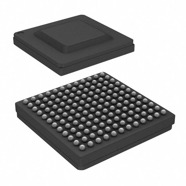
Device Information(1)
PART NUMBER
PACKAGE
BODY SIZE (NOM)
DAC37J82
FCBGA (144)
10.00 mm x 10.00 mm
DAC38J82
FCBGA (144)
10.00 mm x 10.00 mm
(1) For all available packages, see the orderable addendum at
the end of the datasheet.
DAC37J82/DAC38J82
xN
Complex Mixer
(48-bit NCO)
•
•
•
Digital data is input to the device through 1, 2, 4 or 8
configurable serial JESD204B lanes running up to
12.5
Gbps
with
on-chip
termination
and
programmable equalization. The interface allows
JESD204B Subclass 1 SYSREF based deterministic
latency and full synchronization of multiple devices.
JESD204B Interface
•
•
Resolution: 16-Bit
Maximum Sample Rate:
– DAC37J82: 1.6 GSPS
– DAC38J82: 2.5 GSPS
Maximum Input Data Rate: 1.23GSPS
JESD204B Interface
– 8 JESD204B Serial Input Lanes
– 12.5 Gbps Maximum Bit Rate per Lane
– Subclass 1 Multi-DAC synchronization
On-Chip Very Low Jitter PLL
Selectable 1x -16x Interpolation
Independent Complex Mixers with 48-bit NCO/ or
±n×Fs/8
Wideband Digital Quadrature Modulator
Correction
Sinx/x Correction Filters
Fractional Sample Group Delay Correction
Flexible Routing to Four Analog Outputs via
Output Multiplexer
3/4-Wire Serial Control Bus (SPI)
Integrated Temperature Sensor
JTAG Boundary Scan
Pin-compatible with Quad-channel
DAC37J84/DAC38J84
Power Dissipation: 1.1W at 2.5GSPS
Package: 10x10mm, 144-Ball Flip-Chip BGA
8 lanes @ 12.5 Gbps
1
16-bit DAC
RF
16-bit DAC
xN
1
An IMPORTANT NOTICE at the end of this data sheet addresses availability, warranty, changes, use in safety-critical applications,
intellectual property matters and other important disclaimers. PRODUCTION DATA.
�DAC37J82, DAC38J82
SLASE16B – JANUARY 2014 – REVISED MAY 2014
www.ti.com
Table of Contents
1
2
3
4
5
6
Features ..................................................................
Applications ...........................................................
Description .............................................................
Revision History.....................................................
Pin Configuration and Functions .........................
Specifications.........................................................
6.1
6.2
6.3
6.4
6.5
6.6
6.7
6.8
6.9
6.10
7
1
1
1
2
3
6
Absolute Maximum Ratings ...................................... 6
Handling Ratings....................................................... 6
Recommended Operating Conditions....................... 7
Thermal Information .................................................. 7
DC Electrical Characteristics .................................... 7
Digital Electrical Characteristics.............................. 10
AC Electrical Characteristics................................... 11
Timing Requirements .............................................. 13
Switching Characteristics ........................................ 13
Typical Characteristics .......................................... 14
Detailed Description ............................................ 23
7.1 Overview ................................................................. 23
7.2
7.3
7.4
7.5
8
Functional Block Diagram .......................................
Feature Description.................................................
Device Functional Modes........................................
Register Map...........................................................
23
24
55
58
Applications and Implementation .................... 102
8.1 Application Information.......................................... 102
8.2 Typical Applications .............................................. 102
8.3 Initialization Set Up ............................................... 107
9 Power Supply Recommendations.................... 108
10 Layout................................................................. 109
10.1 Layout Guidelines ............................................... 109
10.2 Layout Examples................................................. 110
11 Device and Documentation Support ............... 112
11.1
11.2
11.3
11.4
Related Links ......................................................
Trademarks .........................................................
Electrostatic Discharge Caution ..........................
Glossary ..............................................................
112
112
112
112
12 Mechanical, Packaging, and Orderable
Information ......................................................... 113
4 Revision History
Changes from Revision A (January 2014) to Revision B
•
Changed status from Product Preview to Production Data .................................................................................................... 1
Changes from Original (January 2014) to Revision A
•
2
Page
Page
Changed Pin Configuration .................................................................................................................................................... 3
Submit Documentation Feedback
Copyright © 2014, Texas Instruments Incorporated
Product Folder Links: DAC37J82 DAC38J82
�DAC37J82, DAC38J82
www.ti.com
SLASE16B – JANUARY 2014 – REVISED MAY 2014
Device Comparison Table
(1)
DEVICE
MAXIMUM SAMPLE RATE
PACKAGE DRAWING/TYPE (1)
TA
DAC37J82IAAV
1.6 GSPS
AAV/144-ball flip chip BGA
–40°C to 85°C
DAC38J82IAAV
2.5 GSPS
AAV/144-ball flip chip BGA
–40°C to 85°C
MSL Peak Temperature: Level-3-260C-168 HR
5 Pin Configuration and Functions
144-Ball Flip Chip BGA
AAV Package
(Top View)
A
B
C
D
E
F
G
H
J
K
L
M
12
GND
IOUTAP
IOUTAN
IOUTBN
IOUTBP
GND
GND
IOUTCP
IOUTCN
IOUTDN
IOUTDP
GND
12
11
GND
GND
GND
GND
GND
GND
GND
GND
GND
GND
GND
GND
11
10
DACCLKP
VDDAPLL18 VDDAREF18 VDDADAC33 VDDADAC33
EXTIO
RBIAS
SDIO
SDO
10
9
DACCLKN
VDDAPLL18
LPF
VDDDAC09
VDDDAC09
VDDDAC09
VDDDAC09
VDDDAC09
VDDDAC09
ATEST
SCLK
SDENB
9
8
VDDCLK09
VDDCLK09
GND
GND
GND
GND
GND
GND
GND
RESETB
ALARM
SLEEP
8
7
SYSREFP
SYNCBP
VDDS18
VQPS18
GND
GND
GND
GND
VDDDIG09
VDDIO18
SYNC_N_CD
NC
7
6
SYSREFN
SYNCBN
VDDS18
VQPS18
GND
GND
GND
GND
VDDDIG09
VDDIO18
SYNC_N_AB
NC
6
5
GND
GND
IFORCE
VDDDIG09
GND
GND
GND
GND
VDDDIG09
TXENABLE
TDI
TDO
5
4
GND
GND
VSENSE
VDDDIG09
VDDDIG09
VDDDIG09
VDDDIG09
VDDDIG09
VDDDIG09
TCLK
TMS
GND
4
3
RX7P
GND
GND
VDDDIG09
AMUX1
VDDT09
VDDT09
AMUX0
TRSTB
TESTMODE
GND
RX3P
3
2
RX7N
GND
GND
GND
GND
VDDR18
VDDR18
GND
GND
GND
GND
RX3N
2
1
RX6N
RX6P
RX5P
RX5N
RX4N
RX4P
RX0P
RX0N
RX1N
RX1P
RX2P
RX2N
1
A
B
C
D
E
F
G
VDDADAC33 VDDADAC33 VDDAREF18
H
J
K
L
M
Submit Documentation Feedback
Copyright © 2014, Texas Instruments Incorporated
Product Folder Links: DAC37J82 DAC38J82
3
�DAC37J82, DAC38J82
SLASE16B – JANUARY 2014 – REVISED MAY 2014
www.ti.com
Pin Functions
PIN
NAME
NUMBER
I/O
DESCRIPTION
ALARM
L8
O
CMOS output for ALARM condition. The ALARM output functionality is defined through the
config7 register. Default polarity is active high, but can be changed to active high via config0
alarm_out_pol control bit. If not used it can be left open.
AMUX0
H3
I/O
Analog test pin for SerDes, Lane 0 to Lane 3. It can be left open if not used.
AMUX1
E3
I/O
Analog test pin for SerDes, Lane 4 to Lane 7. It can be left open if not used.
ATEST
K9
I/O
Analog test pin for DAC, references and PLL. It can be left open if not used.
DACCLKP
A10
I
Positive LVPECL clock input for DAC core with Vcm = 0.5V. It can be PLL reference clock or
external DAC sampling rate clock. If not used, DACCLK is self-biased with 100mV differential
at Vcm = 0.5V.
DACCLKN
A9
I
Complementary LVPECL clock input for DAC core. (see the DACCLKP description)
EXTIO
F10
I/O
A12, F12, G12,
M12, A11, B11,
C11, D11, E11,
F11, G11, H11,
J11, K11, L11,
M11, C8, D8, E8,
F8, G8, H8, J8,
E7, F7, G7, H7,
E6, F6, G6, H6,
A5, B5, E5, F5,
G5, H5, A4, B4,
M4, B3, C3, L3,
B2, C2, D2, E2,
H2, J2, K2, L2
I
C5
I/O
Analog test pin for on chip parametric. It can be left open if not used.
IOUTAP
B12
O
A-Channel DAC current output. Must tied to GND if not used.
IOUTAN
C12
O
A-Channel DAC complementary current output. Must tied to GND if not used.
IOUTBP
E12
O
B-Channel DAC current output. Must tied to GND if not used.
IOUTBN
D12
O
B-Channel DAC complementary current output. Must tied to GND if not used.
IOUTCP
H12
O
C-Channel DAC current output. Must tied to GND if not used.
IOUTCN
J12
O
C-Channel DAC complementary current output. Must tied to GND if not used.
IOUTDP
L12
O
D-Channel DAC current output. Must tied to GND if not used.
IOUTDN
K12
O
D-Channel DAC complementary current output. Must tied to GND if not used.
LPF
C9
I/O
External PLL loop filter connection. It can be left open if not used.
G10
O
Full-scale output current bias. Change the full-scale output current through coarse_dac(3:0).
Expected to be 1.92kΩ to GND.
RESETB
K8
I
Active low input for chip RESET, which resets all the programming registers to their default
state. Internal pull-up. It can be left open if not used.
RX0P
G1
I
CML SerDes interface lane 0 input, positive, expected to be AC coupled. It can be left open if
not used.
RX0N
H1
I
CML SerDes interface lane 0 input, negative, expected to be AC coupled. It can be left open if
not used.
RX1P
K1
I
CML SerDes interface lane 1 input, positive, expected to be AC coupled. It can be left open if
not used.
RX1N
J1
I
CML SerDes interface lane 1 input, negative, expected to be AC coupled. It can be left open if
not used.
RX2P
L1
I
CML SerDes interface lane 2 input, positive, expected to be AC coupled. It can be left open if
not used.
RX2N
M1
I
CML SerDes interface lane 2 input, negative, expected to be AC coupled. It can be left open if
not used.
RX3P
M3
I
CML SerDes interface lane 3 input, positive, expected to be AC coupled. It can be left open if
not used.
GND
IFORCE
RBIAS
4
Used as external reference input when internal reference is disabled through config27
extref_ena = ‘1’. Used as internal reference output when config27 extref_ena = ‘0’ (default).
Requires a 0.1 μF decoupling capacitor to analog GND when used as reference output. It can
be left open if not used.
These pins are ground for all supplies.
Submit Documentation Feedback
Copyright © 2014, Texas Instruments Incorporated
Product Folder Links: DAC37J82 DAC38J82
�DAC37J82, DAC38J82
www.ti.com
SLASE16B – JANUARY 2014 – REVISED MAY 2014
Pin Functions (continued)
PIN
NAME
NUMBER
I/O
DESCRIPTION
RX3N
M2
I
CML SerDes interface lane 3 input, negative, expected to be AC coupled. It can be left open if
not used.
RX4P
F1
I
CML SerDes interface lane 4 input, positive, expected to be AC coupled. It can be left open if
not used.
RX4N
E1
I
CML SerDes interface lane 4 input, negative, expected to be AC coupled. It can be left open if
not used.
RX5P
C1
I
CML SerDes interface lane 5 input, positive, expected to be AC coupled. It can be left open if
not used.
RX5N
D1
I
CML SerDes interface lane 5 input, negative, expected to be AC coupled. It can be left open if
not used.
RX6P
B1
I
CML SerDes interface lane 6 input, positive, expected to be AC coupled. It can be left open if
not used.
RX6N
A1
I
CML SerDes interface lane 6 input, negative, expected to be AC coupled. It can be left open if
not used.
RX7P
A3
I
CML SerDes interface lane 7 input, positive, expected to be AC coupled. It can be left open if
not used.
RX7N
A2
I
CML SerDes interface lane 7 input, negative, expected to be AC coupled. It can be left open if
not used.
SYSREFP
A7
I
LVPECL SYSREF positive input with Vcm = 0.5V. This positive/negative pair is captured with
the rising edge of DACCLKP/N. It is used for JESD204B Subclass 1 deterministic latency and
multiple DAC synchronization, which can be periodic or pulsed. If not used, it is self-biased with
100mV differential at Vcm = 0.5V.
SYSREFN
A6
I
LVPECL SYSREF negative input with Vcm = 0.5V. (See the SYSREFP description)
SCLK
L9
I
Serial interface clock. Internal pull-down. It can be left open if not used.
SDENB
M9
I
Active low serial data enable, always an input to the DAC37J82/DAC38J82. Internal pull-up. It
can be left open if not used.
SDIO
L10
I/O
Serial interface data. Bi-directional in 3-pin mode (default) and 4-pin mode. Internal pull-down.
It can be left open if not used.
SDO
M10
O
Uni-directional serial interface data in 4-pin mode. The SDO pin is tri-stated in 3-pin interface
mode (default). It can be left open if not used.
SLEEP
M8
I
Active high asynchronous hardware power-down input. Internal pull-down. It can be left open if
not used.
SYNCBP
B7
O
Synchronization request to transmitter, LVDS positive output. It can be left open if not used.
SYNCBN
B6
O
Synchronization request to transmitter, LVDS negative output. It can be left open if not used.
SYNC_N_AB
L6
O
Synchronization request to transmitter, CMOS output. Defaults to link 0, but can be
programmable for any link. It can be left open if not used.
SYNC_N_CD
L7
O
Synchronization request to transmitter, CMOS output. Defaults to link 1, but can be
programmable for any link. It can be left open if not used.
TCLK
K4
I
JTAG test clock. It can be left open if not used.
TDI
L5
I
JTAG test data in. It can be left open if not used.
TDO
M5
O
JTAG test data out. It can be left open if not used.
TMS
L4
I
JTAG test mode select. It can be left open if not used.
TRSTB
J3
I
JTAG test reset. Must be tied to GND to hold the JTAG state machine status reset if the JTAG
port is not used.
TXENABLE
K5
I
To enable analog output data transmission, set sif_txenable in register config3 to “1” or pull
CMOS TXENABLE pin to high. Transmit enable active high input. Internal pull-down. To
disable analog output, set sif_txenable to “0” and pull CMOS TXENABLE pin to low. The DAC
output is forced to midscale. It can be left open if not used.
TESTMODE
K3
O
This pin is used for factory testing. Internal pull-down. It can be left open if not used.
VDDADAC33
D10, E10, H10,
J10,
I
Analog supply voltage. (3.3V)
VDDAPLL18
B10, B9
I
PLL analog supply voltage. (1.8V)
VDDAREF18
C10, K10
I
Analog reference supply voltage (1.8V)
Submit Documentation Feedback
Copyright © 2014, Texas Instruments Incorporated
Product Folder Links: DAC37J82 DAC38J82
5
�DAC37J82, DAC38J82
SLASE16B – JANUARY 2014 – REVISED MAY 2014
www.ti.com
Pin Functions (continued)
PIN
NAME
NUMBER
I/O
DESCRIPTION
VDDCLK09
A8, B8
I
Internal clock buffer supply voltage (0.9V). It is recommended to isolate this supply from
VDDDIG09.
VDDDAC09
D9, E9, F9, G9,
H9, J9
I
DAC core supply voltage. (0.9V). It is recommended to isolate this supply from VDDDIG09.
VDDDIG09
J7, J6, D5, J5,
D4, E4, F4, G4,
H4, J4, D3
I
Digital supply voltage. (0.9V). It is recommended to isolate this supply from VDDCLK09 and
VDDDAC09.
VDDIO18
K7, K6
I
Supply voltage for all digital I/O and CMOS I/O. (1.8V)
VDDR18
F2, G2
I
Supply voltage for SerDes (1.8V)
VDDS18
C7, C6
I
Supply voltage for LVDS SYNCBP/N (1.8V)
VDDT09
F3, G3
I
Supply voltage for SerDes termination (0.9V)
VQPS18
D7, D6
I
Fuse supply voltage. This supply pin is also used for factory fuse programming. Connect to
1.8V.
VSENSE
C4
I/O
Analog test pin for on chip parametric. It can be left open if not used.
6 Specifications
6.1 Absolute Maximum Ratings
over operating free-air temperature range (unless otherwise noted) (1)
Supply
voltage (2)
MIN
MAX
VDDDAC09, VDDDIG09
–0.3
1.3
V
VDDCLK09
–0.3
1.3
V
VDDT09
–0.3
1.3
V
VDDR18, VDDIO18, VDDS18, VQPS18
–0.3
2.45
V
VDDAPLL18, VDDAREF18
–0.3
2.45
V
VDDADAC33
Pin voltage (2)
–0.3
4.0
V
RX[7..0]P/N
–0.5 V
VDDT09 + 0.5 V
V
SDENB, SCLK, SDIO, SDO, TXENA, ALARM, RESETB, SLEEP, TMS,
TCLK, TDI, TDO, TRSTB, TESTMODE, SYNC_N_AB, SYNC_N_CD
–0.5 V
VDDIO18 + 0.5 V
V
DACCLKP/N, SYSREFP/N
–0.5 V VDDAPLL18 + 0.5 V
V
SYNCBP/N
–0.5 V
VDDS18 + 0.5 V
V
LPF
–0.5 V VDDAPLL18 + 0.5 V
V
IOUTAP/N, IOUTBP/N, IOUTCP/N, IOUTDP/N
–0.5 V
1.0 V
V
RBIAS, EXTIO, ATEST
–0.5 V VDDAREF18 + 0.5 V
V
IFORCE, VSENSE
–0.5 V
VDDDIG09 + 0.5 V
V
AMUX1, AMUX0
–0.5 V
VDDT09 + 0.5 V
Peak input current (any input)
Peak total input current (all inputs)
Absolute maximum junction temperature TJ
Operating free-air temperature range, TA: DAC37J82/DAC38J82
(1)
(2)
UNIT
–40
V
20
mA
–30
mA
150
°C
85
°C
Stresses beyond those listed under absolute maximum ratings may cause permanent damage to the device. These are stress ratings
only and functional operation of these or any other conditions beyond those indicated under “recommended operating conditions” is not
implied. Exposure to absolute-maximum-rated conditions for extended periods may affect device reliability.
Measured with respect to GND.
6.2 Handling Ratings
Tstg
6
Storage temperature range
Submit Documentation Feedback
MIN
MAX
UNIT
–65
150
°C
Copyright © 2014, Texas Instruments Incorporated
Product Folder Links: DAC37J82 DAC38J82
�DAC37J82, DAC38J82
www.ti.com
SLASE16B – JANUARY 2014 – REVISED MAY 2014
6.3 Recommended Operating Conditions
MIN
TJ
TA
(1)
NOM MAX
Recommended operating junction temperature (1)
UNIT
105
Maximum rated operating junction temperature
125
Recommended free-air temperature
-40
°C
°C
25
85
°C
Prolonged use at this junction temperature may increase the device failure-in-time (FIT) rate.
6.4 Thermal Information
DAC3xJ82
THERMAL CONDUCTIVITY (1)
RθJA
Theta junction-to-ambient (still air)
31.4
RθJB
Theta junction-to-board
12.6
RθJC
Theta junction-to-case, top
1.8
ψJT
Psi junction-to-top of package
0.2
ψJB
Psi junction-to-bottom of package
12
(1)
UNIT
AAV (144 PINS)
°C/W
Air flow or heat sinking reduces θJA and may be required for sustained operation at 85° and maximum operating conditions.
6.5 DC Electrical Characteristics
Typical values at TA = 25°C, full temperature range is TMIN = -40°C to TMAX = 85°C, nominal supplies, unless otherwise noted.
PARAMETER
TEST CONDITIONS
Resolution
DAC37J82
MIN
TYP
DAC38J82
MAX
16
MIN
TYP
MAX
16
UNIT
Bits
DC ACCURACY
DNL
Differential nonlinearity
INL
Integral nonlinearity
1 LSB = IOUTFS/216
±4
±4
LSB
±6
±6
LSB
ANALOG OUTPUT
Coarse gain linearity
Offset error
Gain error
Gain mismatch
±0.04
±0.04
LSB
±0.001
±0.001
%FSR
With external reference
±2
±2
With internal reference
±2
±2
Mid code offset
With internal reference
±2
Full scale output current
20
Output compliance range
–0.5
Output resistance
%FSR
±2
30
0.6
20
–0.5
%FSR
30
mA
0.6
V
300
300
kΩ
5
5
pF
Output capacitance
REFERENCE OUTPUT
VREF
Reference output voltage
0.9
0.9
V
Reference output current (1)
100
100
nA
REFERENCE INPUT
VEXTIO
Input voltage range
External reference mode
0.1
0.9
Input resistance
1
0.1
0.9
1
V
1
1
MΩ
50
50
pF
±1
±1
Ppm/°C
With external reference
±15
±15
With internal reference
±30
±30
±8
±8
Input capacitance
TEMPERATURE COEFFICIENTS
Offset drift
Gain drift
Reference voltage drift
(1)
ppm/°C
ppm/°C
Use an external buffer amplifier with high impedance input to drive any external load.
Submit Documentation Feedback
Copyright © 2014, Texas Instruments Incorporated
Product Folder Links: DAC37J82 DAC38J82
7
�DAC37J82, DAC38J82
SLASE16B – JANUARY 2014 – REVISED MAY 2014
www.ti.com
DC Electrical Characteristics (continued)
Typical values at TA = 25°C, full temperature range is TMIN = -40°C to TMAX = 85°C, nominal supplies, unless otherwise noted.
PARAMETER
TEST CONDITIONS
DAC37J82
DAC38J82
MIN
TYP
MAX
MIN
TYP
MAX
VDDADAC33
3.15
3.3
3.45
3.15
3.3
3.45
VDDAPLL18, VDDAREF18,
VDDS18, VQPS18, VDDR18
1.71
1.8
1.89
1.71
1.8
1.89
VDDIO18
1.71
1.8
1.89
1.71
1.8
1.89
VDDDIG09, VDDDAC09,
VDDCLK09, VDDT09
0.85
0.9
0.95
0.85
0.9
0.95
UNIT
POWER SUPPLY
PSRR
Power Supply Rejection Ratio
DC tested
±0.2
±0.2
V
V
V
V
%FSR/V
POWER CONSUMPTION
I(VDDADAC33)
Analog supply current
I(VDDDIG09)
Digital supply current
I(VDDDAC09)
DAC supply current
I(VDDCLK09)
Clock supply current
I(VDDT09)
SerDes core supply current
I(VDDR18)
SerDes analog supply current
I(VDD18)
Other 1.8V supply current
P
Power dissipation
I(VDDADAC33)
Analog supply current
I(VDDDIG09)
Digital supply current
I(VDDDAC09)
DAC supply current
I(VDDCLK09)
Clock supply current
I(VDDT09)
SerDes core supply current
I(VDDR18)
SerDes analog supply current
I(VDD18)
Other 1.8V supply current
P
Power dissipation
I(VDDADAC33)
Analog supply current
I(VDDDIG09)
Digital supply current
I(VDDDAC09)
DAC supply current
I(VDDCLK09)
Clock supply current
I(VDDT09)
SerDes core supply current
I(VDDR18)
SerDes analog supply current
I(VDD18)
Other 1.8V supply current
P
Power dissipation
I(VDDADAC33)
Analog supply current
I(VDDDIG09)
Digital supply current
I(VDDDAC09)
DAC supply current
I(VDDCLK09)
Clock supply current
I(VDDT09)
SerDes core supply current
I(VDDR18)
SerDes analog supply current
I(VDD18)
Other 1.8V supply current
P
Power dissipation
(2)
8
MODE 1:(DAC38J82)
fDAC=2.46GSPS, 2x
interpolation,
NCO on, QMC on, inverse
sinc on,
GDC off, PAP off, PLL on,
LMF=421,
SerDes rate = 12.3GSPS,
20mA FS output,
IF=150MHz.
MODE 2: (DAC37J82)
fDAC=1.6GSPS, 2x
interpolation,
NCO on, QMC on, invsinc on,
GDC off, PAP off, PLL on,
LMF=421,
SerDes rate = 8GSPS,
20mA FS output, IF=150MHz.
MODE 3:
fDAC=1.47456GSPS, 2x
interpolation,
NCO on, QMC off, invsinc off,
GDC off,
PAP off, PLL off, LMF=421,
SerDes rate = 7.3728GSPS,
20mA FS output, IF=150MHz.
MODE 4:
fDAC=1.47456GSPS, 4x
interpolation,
NCO on, QMC off, invsinc off,
GDC off, PAP off, PLL off,
LMF=222,
SerDes rate = 7.3728GSPS,
20mA FS output, IF=150MHz.
-
64
80
-
628
800
-
13
25
-
86
120
-
168
250
-
18
35
-
53
80
-
1144
1290 (2)
64
64
418
418
10
10
57
57
139
139
12
12
50
50
884
884
64
64
363
363
10
10
50
50
135
135
12
12
30
30
789
789
64
64
312
312
10
10
50
50
76
76
12
12
30
30
690
690
mA
mW
mA
mW
mA
mW
mA
mW
The MAX power limit is set separately which is NOT equal to the power consumption when all of the power supplies are at the MAX
current.
Submit Documentation Feedback
Copyright © 2014, Texas Instruments Incorporated
Product Folder Links: DAC37J82 DAC38J82
�DAC37J82, DAC38J82
www.ti.com
SLASE16B – JANUARY 2014 – REVISED MAY 2014
DC Electrical Characteristics (continued)
Typical values at TA = 25°C, full temperature range is TMIN = -40°C to TMAX = 85°C, nominal supplies, unless otherwise noted.
PARAMETER
TEST CONDITIONS
DAC37J82
MIN
TYP
DAC38J82
MAX
MIN
TYP
I(VDDADAC33)
Analog supply current
13
13
I(VDDDIG09)
Digital supply current
263
263
I(VDDDAC09)
DAC supply current
I(VDDCLK09)
Clock supply current
I(VDDT09)
SerDes core supply current
I(VDDR18)
SerDes analog supply current
I(VDD18)
Other 1.8V supply current
P
Power dissipation
I(VDDADAC33)
Analog supply current
I(VDDDIG09)
Digital supply current
I(VDDDAC09)
DAC supply current
I(VDDCLK09)
Clock supply current
I(VDDT09)
SerDes core supply current
I(VDDR18)
SerDes analog supply current
I(VDD18)
Other 1.8V supply current
P
Power dissipation
I(VDDADAC33)
Analog supply current
I(VDDDIG09)
Digital supply current
I(VDDDAC09)
DAC supply current
I(VDDCLK09)
Clock supply current
I(VDDT09)
SerDes core supply current
I(VDDR18)
SerDes analog supply current
I(VDD18)
Other 1.8V supply current
P
Power dissipation
I(VDDADAC33)
Analog supply current
I(VDDDIG09)
Digital supply current
I(VDDDAC09)
DAC supply current
I(VDDCLK09)
Clock supply current
I(VDDT09)
SerDes core supply current
I(VDDR18)
SerDes analog supply current
I(VDD18)
Other 1.8V supply current
P
Power dissipation
I(VDDADAC33)
Analog supply current
I(VDDDIG09)
Digital supply current
I(VDDDAC09)
DAC supply current
I(VDDCLK09)
Clock supply current
I(VDDT09)
SerDes core supply current
I(VDDR18)
SerDes analog supply current
I(VDD18)
Other 1.8V supply current
P
Power dissipation
I(VDDADAC33)
MODE 5:
fDAC=1.47456GSPS, x4,
NCO off, QMC off, invsinc off,
GDC off, PAP off,
PLL off, LMF=222,
SerDes rate = 7.3728GSPS,
DAC output in sleep mode.
MODE 6:
fDAC=1000MSPS, 2x
interpolation,
NCO off, QMC off, invsinc off,
GDC off, PAP off, PLL on,
LMF=222, SerDes rate =
10GSPS,
20mA FS output, IF=150MHz.
MODE 7:
fDAC=1000MSPS, 2x
interpolation,
NCO off, QMC off invsinc off,
GDC off,
PAP off, PLL off, LMF=222,
SerDes rate = 10GSPS,
20mA FS output, IF=150MHz.
MODE 8:
fDAC=625MSPS, 2x
interpolation,
NCO off, QMC off, invsinc off,
GDC off,
PAP off, PLL off, LMF=421,
SerDes rate = 3.125GSPS,
20mA FS output, IF=20MHz.
MODE 9:
fDAC=1.23GSPS, no
interpolation,
NCO off, QMC off, invsinc off,
GDC off,
PAP off, PLL off, LMF=421,
SerDes rate = 12.3GSPS,
20mA FS output, IF=150MHz;
8
8
50
50
76
76
12
12
26
26
469
469
64
64
257
257
8
8
36
36
85
85
15
15
50
50
676
676
64
64
256
256
8
8
35
35
85
85
15
15
29
29
636
636
64
64
195
195
4
4
22
22
119
119
11
11
25
25
582
582
64
64
311
311
10
10
42
42
165
165
18
18
29
29
771
771
Analog supply current
5
5
I(VDDDIG09)
Digital supply current
76
76
I(VDDDAC09)
DAC supply current
1
1
I(VDDCLK09)
Clock supply current
1
1
I(VDDT09)
SerDes core supply current
9
9
I(VDDR18)
SerDes analog supply current
I(VDD18)
Other 1.8V supply current
P
Power dissipation
MODE 10:
Power down mode, no clock,
DAC in sleep mode,
SerDes in sleep mode
0
0
10
10
112
112
MAX
UNIT
mA
mW
mA
mW
mA
mW
mA
mW
mA
mW
mA
mW
Submit Documentation Feedback
Copyright © 2014, Texas Instruments Incorporated
Product Folder Links: DAC37J82 DAC38J82
9
�DAC37J82, DAC38J82
SLASE16B – JANUARY 2014 – REVISED MAY 2014
www.ti.com
6.6 Digital Electrical Characteristics
Typical values at TA = 25°C, full temperature range is TMIN = –40°C to TMAX = 85°C, nominal supplies, unless otherwise noted.
PARAMETER
TEST CONDITIONS
DAC37J82
MIN
TYP
DAC38J82
MAX
MIN
1200
50
TYP
MAX
UNIT
CML SERDES INPUTS: RX[7:0]P/N
VDIFF
VCOM
Receiver input amplitude
50
1200
Input common mode
(TERM=111)
600
600
Input common mode
(TERM=001)
700
700
Input common mode
(TERM=100)
0
0
Input common mode
(TERM=101)
250
250
ZDIFF
Internal differential
termination
fDATA
Serdes bit rate
mV
mV
85
100
0.78125
115
85
12.5
0.78125
100
115
Ω
12.5
Gbps
LVPECL INPUTS: SYSREFP/N
VCOM
Input common mode voltage
VIDPP
Differential input peak-topeak voltage
ZT
Internal termination
CL
Input capacitance
0.5
400
800
400
0.5
V
800
mV
100
100
Ω
2
2
pF
0.5
0.5
V
800
mV
LVPECL INPUTS: DACCLKP/N
VCOM
Input common mode voltage
VIDPP
Differential input peak-topeak voltage
ZT
Internal termination
CL
Input capacitance
400
Duty cycle
fDACCLK
800
400
100
100
Ω
2
2
pF
40%
60%
DACCLKP/N Input
Frequency
40%
60%
1.6
2.5
GHz
LVDS OUTPUTS: SYNCBP/N
VCOM
Output common mode
voltage
1.2
1.2
V
ZT
Internal termination
100
100
Ω
VOD
Differential output voltage
swing
0.5
0.5
V
CMOS INTERFACE: SDENB, SCLK, SDIO, SDO, TXENA, ALARM, RESETB, SLEEP, TMS, TCLK, TDI, TDO, TRSTB, TESTMODE, SYNC_N_AB,
SYNC_N_CD
0.7 x
VDDIO1
8
0.7 x
VDDIO1
8
VIH
High-level input voltage
VIL
Low-level input voltage
IIH
High-level input current
-40
40
IIL
Low-level input current
-40
40
CI
CMOS Input capacitance
VOH
VOL
10
0.3 x
VDDI
O18
0.3 x
VDDIO
18
V
-40
40
µA
-40
40
µA
2
2
Iload =–100 μA
VDDIO1
8 – 0.2
VDDIO1
8 – 0.2
Iload = –2 mA
0.8 x
VDDIO1
8
0.8 x
VDDIO1
8
ALARM, SDO, SDIO, TDO
ALARM, SDO, SDIO, TDO
V
pF
V
Iload = 100 μA
0.2
0.2
Iload = 2 mA
0.5
0.5
Submit Documentation Feedback
V
Copyright © 2014, Texas Instruments Incorporated
Product Folder Links: DAC37J82 DAC38J82
�DAC37J82, DAC38J82
www.ti.com
SLASE16B – JANUARY 2014 – REVISED MAY 2014
Digital Electrical Characteristics (continued)
Typical values at TA = 25°C, full temperature range is TMIN = –40°C to TMAX = 85°C, nominal supplies, unless otherwise noted.
PARAMETER
TEST CONDITIONS
DAC37J82
MIN
TYP
DAC38J82
MAX
MIN
TYP
UNIT
MAX
PHASE LOCKED LOOP
PLL/VCO operating frequency
pll_vcosel = '1', pll_vco = '010001'(17),
pll_vcoitune = '10', VCO Frequency =
3932.16MHz
Assured
Assured
pll_vcosel = '1', pll_vco = '011111'(31),
pll_vcoitune = '10', VCO Frequency =
4120MHz
Assured
Assured
pll_vcosel = '1', pll_vco = '110010'(50),
pll_vcoitune = '10', VCO Frequency =
4423.68MHz
Assured
Assured
pll_vcosel = '0', pll_vco = '001101'(13),
pll_vcoitune = '11', VCO Frequency =
4608MHz
Assured
Assured
pll_vcosel = '0', pll_vco = '011010'(26),
pll_vcoitune = '11', VCO Frequency =
4800MHz
Assured
Assured
pll_vcosel = '0', pll_vco = '100001'(33),
pll_vcoitune = '11', VCO Frequency =
4915.2MHz
Assured
Assured
pll_vcosel = '0', pll_vco = '100110'(38),
pll_vcoitune = '11', VCO Frequency =
5000MHz
Assured
Assured
6.7 AC Electrical Characteristics
Typical values at TA = 25°C, full temperature range is TMIN = –40°C to TMAX = 85°C, nominal supplies, unless otherwise noted.
PARAMETER
ANALOG OUTPUT
fDAC
TEST CONDITIONS / COMMENTS
DAC37J82
MIN
DAC38J82
MAX
MIN
TYP
UNIT
MAX
(1)
Maximum DAC rate
4x or higher interpolation
1600
2500
2x interpolation
1600
2460
1x interpolation
1230
1230
No interpolation, FIFO off, Mixer off, QMC off, Inverse
sinc off
Digital latency
(F=2, 2x interpolation)
(1)
TYP
11
MSPS
11
2x Interpolation
83
83
4x Interpolation
211
211
8x Interpolation
483
483
16x Interpolation
1051
1051
NCO
48
48
QMC
32
32
Inverse Sinc
36
36
PA Protection (pap_dlylen_sel = "0")
68
68
Dithering
0
0
Complex Summation
0
0
Coarse Fractional Delay
51
51
Fine Fractional Delay
52
52
DAC clock
cycles
Measured single ended into 50 Ω load.
Submit Documentation Feedback
Copyright © 2014, Texas Instruments Incorporated
Product Folder Links: DAC37J82 DAC38J82
11
�DAC37J82, DAC38J82
SLASE16B – JANUARY 2014 – REVISED MAY 2014
www.ti.com
AC Electrical Characteristics (continued)
Typical values at TA = 25°C, full temperature range is TMIN = –40°C to TMAX = 85°C, nominal supplies, unless otherwise noted.
PARAMETER
AC PERFORMANCE
SFDR
IMD3
ACLR (3)
Spurious free dynamic
(0 to fDAC/2)
Third-order two-tone
intermodulation distortion
Each tone at –6dBFS
12
TYP
DAC38J82
MAX
MIN
TYP
fDAC = 2.5 GSPS, fOUT = 20 MHz, 0 dBFS
-
79
fDAC = 2.5 GSPS, fOUT = 70 MHz, 0dBFS
-
78
fDAC = 2.5 GSPS, fOUT = 150 MHz, 0 dBFS
-
72
fDAC = 2.5 GSPS, fOUT = 230 MHz, 0dBFS
-
67
fDAC = 2.5 GSPS, fOUT = 20 MHz, -12 dBFS
-
79
fDAC = 2.5 GSPS, fOUT = 70 MHz, –12dBFS
-
75
fDAC = 2.5 GSPS, fOUT = 150 MHz, -12 dBFS
-
70
fDAC = 2.5 GSPS, fOUT = 230 MHz, –12dBFS
-
65
fDAC = 1.6 GSPS, fOUT = 20 MHz, 0 dBFS
81
81
fDAC = 1.6 GSPS, fOUT = 70 MHz, 0 dBFS
77
77
fDAC = 1.6 GSPS, fOUT = 150 MHz, 0 dBFS
72
72
fDAC = 1.6 GSPS, fOUT = 230 MHz, 0 dBFS
68
68
fDAC = 1.6 GSPS, fOUT = 20 MHz, -12 dBFS
76
76
fDAC = 1.6 GSPS, fOUT = 70 MHz, –12 dBFS
72
72
fDAC = 1.6 GSPS, fOUT = 150 MHz, -12 dBFS
67
67
fDAC = 1.6 GSPS, fOUT = 230 MHz, –12 dBFS
64
64
fDAC = 2.5 GSPS, fOUT = 70 ± 0.5 MHz
-
83
fDAC = 2.5 GSPS, fOUT = 150 ± 0.5 MHz
-
75
fDAC = 2.5 GSPS, fOUT = 230 ± 0.5 MHz
-
70
fDAC = 2.0 GSPS, fOUT = 70 ± 0.5 MHz
-
86
fDAC = 2.0 GSPS, fOUT = 150 ± 0.5 MHz
-
78
fDAC = 2.0 GSPS, fOUT = 230 ± 0.5 MHz
-
73
fDAC = 1.6 GSPS, fOUT = 70 ± 0.5 MHz
83
83
fDAC = 1.6 GSPS, fOUT = 150 ± 0.5 MHz
73
73
fDAC = 1.6 GSPS, fOUT = 230 ± 0.5 MHz
66
66
fDAC = 2.5 GSPS, fOUT = 70 MHz
-
-161
fDAC = 2.5 GSPS, fOUT = 150 MHz
-
–159
fDAC = 2.5 GSPS, fOUT = 230 MHz
-
-157
fDAC = 2.0 GSPS, fOUT = 70 MHz
-
-161
fDAC = 2.0 GSPS, fOUT = 150 MHz
-
-160
fDAC = 2.0 GSPS, fOUT = 230 MHz
-
-158
fDAC = 1.6 GSPS, fOUT = 70 MHz
-161
-161
fDAC = 1.6 GSPS, fOUT = 150 MHz
-159
-159
fDAC = 1.6 GSPS, fOUT = 230 MHz
-157
-157
fDAC = 2.4576 GSPS, fOUT = 70 MHz
-
82
fDAC = 2.4576 GSPS, fOUT = 150 MHz
-
80
fDAC = 2.4576 GSPS, fOUT = 230 MHz
-
78
fDAC = 1.96608 GSPS, fOUT = 70 MHz
-
82
-
80
-
77
fDAC = 1.47456 GSPS, fOUT = 70 MHz
82
82
fDAC = 1.47456 GSPS, fOUT = 150 MHz
80
80
fDAC = 1.47456 GSPS, fOUT = 230 MHz
76
76
fDAC = 2.5 GSPS, fOUT = 20 MHz
-
93
fDAC = 1.6 GSPS, fOUT = 20 MHz
93
93
Adjacent channel leakage
fDAC = 1.96608 GSPS, fOUT = 150 MHz
ratio, single carrier
fDAC = 1.96608 GSPS, fOUT = 230 MHz
Channel isolation
(2)
(3)
DAC37J82
MIN
MAX
UNIT
(2)
Noise spectral density (2)
Tone at –6dBFS
NSD
TEST CONDITIONS / COMMENTS
dBc
dBc
dBFS/Hz
dBc
dBc
2:1 transformer output termination, 50 Ω doubly terminated load.
Single carrier, W-CDMA with 3.84 MHz BW, 5-MHz spacing, centered at IF. TESTMODEL 1, 10 ms
Submit Documentation Feedback
Copyright © 2014, Texas Instruments Incorporated
Product Folder Links: DAC37J82 DAC38J82
�DAC37J82, DAC38J82
www.ti.com
SLASE16B – JANUARY 2014 – REVISED MAY 2014
6.8 Timing Requirements
Typical values at TA = 25°C, full temperature range is TMIN = –40°C to TMAX = 85°C, nominal supplies, unless otherwise noted.
PARAMETER
TEST CONDITIONS
DAC37J82
MIN
TYP
DAC38J82
MAX
MIN
TYP
MAX
UNIT
DIGITAL INPUT TIMING SPECIFICATIONS
TIMING SYSREF INPUT: DACCLKP/N RISING EDGE LATCHING
Setup time, SYSREFP/N
ts(SYSREF) valid to rising edge of
DACCLKP/N
50
50
ps
Hold time, SYSREF/N valid
th(SYSREF) after rising edge of
DACCLKP/N
50
50
ps
TIMING SERIAL PORT
ts(SDENB)
Setup time, SDENB to rising
edge of SCLK
20
20
ns
ts(SDIO)
Setup time, SDIO valid to
rising edge of SCLK
10
10
ns
th(SDIO)
Hold time, SDIO valid to
rising edge of SCLK
5
5
ns
t(SCLK)
Period of SCLK
1
1
µs
100
100
ns
td(Data)
Data output delay after falling
edge of SCLK
10
10
ns
tRESET
Minimum RESETB
pulsewidth
25
25
ns
ns
Register config7 read
(temperature sensor read)
All other registers
ANALOG OUTPUT
ts(DAC)
Powerup Time
(1)
(1)
Output settling time to 0.1%
Transition: Code 0x0000 to 0xFFFF
10
10
DAC wake-up time
IOUT current settling to 1% of IOUTFS from
deep sleep
90
90
DAC sleep time
IOUT current settling to less than 1% of
IOUTFS in deep sleep
90
90
µs
Measured single ended into 50 Ω load.
6.9 Switching Characteristics
Typical values at TA = 25°C, full temperature range is TMIN = –40°C to TMAX = 85°C, nominal supplies, unless otherwise noted.
PARAMETER
ANALOG OUTPUT
TEST CONDITIONS
DAC37J82
MIN
TYP
DAC38J82
MAX
MIN
TYP
MAX
UNIT
(1)
Output propagation delay
tpd
DAC outputs are updated on the falling
edge of DAC clock. Does not include
Digital Latency (see below).
2
2
ns
tr(IOUT)
Output rise time 10% to
90%
50
50
ps
tf(IOUT)
Output fall time 90% to
10%
50
50
ps
(1)
Measured single ended into 50 Ω load.
Submit Documentation Feedback
Copyright © 2014, Texas Instruments Incorporated
Product Folder Links: DAC37J82 DAC38J82
13
�DAC37J82, DAC38J82
SLASE16B – JANUARY 2014 – REVISED MAY 2014
www.ti.com
6.10 Typical Characteristics
Unless otherwise noted, all plots are at TA = 25°C, nominal supply voltages, fDAC = 2460MSPS, 2x interpolation, 0dBFS digital
input, 20mA full scale output current with 2:1 transformer, LMF = 421 and PLL is disabled.
6
Differential Nonlinearity Error (LSB)
Integral Nonlinearity Error (LSB)
5
4
3
2
1
0
-1
-2
-3
-4
0
10000
20000
30000 40000
Code
50000
60000
4
3.5
3
2.5
2
1.5
1
0.5
0
-0.5
-1
-1.5
-2
-2.5
-3
-3.5
70000
0
10000
D001
Figure 1. Integral Nonlinearity
Second Harmonic Distortion (dBc)
70
SFDR (dBc)
50000
60000
70000
D001
100
80
60
50
fDAC = 2460MSPS, 0dBFS
fDAC = 2460MSPS, -6dBFS
fDAC = 2460MSPS, -12dBFS
fDAC = 1600MSPS, 0dBFS
fDAC = 1600MSPS, -6dBFS
fDAC = 1600MSPS, -12dBFS
40
30
0dBFS
-6dBFS
-12dBFS
90
80
70
60
50
40
30
20
0
50
100
150 200 250 300 350
Output Frequency (MHz)
400
450
0
500
50
100
D001
Figure 3. SFDR vs Output Frequency Over Input Scale
150 200 250 300 350
Output Frequency (MHz)
400
450
500
D001
Figure 4. Second Harmonic Distortion vs Output Frequency
Over Input Scale
100
100
0dBFS
-6dBFS
-12dBFS
90
fdata = 1230MSPS, 2x interpolation
fdata = 625MSPS, 4x interpolation
fdata = 312.5MSPS, 8x interpolation
fdata = 156.25MSPS, 16x interpolation
90
80
80
SFDR (dBc)
Third Harmonic Distortion (dBc)
30000 40000
Code
Figure 2. Differential Nonlinearity
90
70
60
70
60
50
50
40
40
30
30
0
50
100
150 200 250 300 350
Output Frequency (MHz)
400
450
500
0
50
100
D001
Figure 5. Third Harmonic Distortion vs Output Frequency
Over Input Scale
14
20000
150 200 250 300 350
Output Frequency (MHz)
400
450
500
D001
Figure 6. SFDR vs Output Frequency Over Interpolation
Submit Documentation Feedback
Copyright © 2014, Texas Instruments Incorporated
Product Folder Links: DAC37J82 DAC38J82
�DAC37J82, DAC38J82
www.ti.com
SLASE16B – JANUARY 2014 – REVISED MAY 2014
Typical Characteristics (continued)
Unless otherwise noted, all plots are at TA = 25°C, nominal supply voltages, fDAC = 2460MSPS, 2x interpolation, 0dBFS digital
input, 20mA full scale output current with 2:1 transformer, LMF = 421 and PLL is disabled.
100
100
fDAC = 2460MSPS
fDAC = 2000MSPS
fDAC = 1600MSPS
fDAC = 1250MSPS
90
80
SFDR (dBc)
SFDR (dBc)
80
IoutFS = 30mA, w/ 2:1 transformer
IoutFS = 20mA, w/ 2:1 transformer
IoutFS = 10mA, w/ 2:1 transformer
90
70
60
70
60
50
50
40
40
30
30
0
50
100
150 200 250 300 350
Output Frequency (MHz)
400
450
500
0
Figure 7. SFDR vs Output Frequency Over fDAC
100
150 200 250 300 350
Output Frequency (MHz)
400
450
500
D001
Figure 8. SFDR vs Output Frequency Over IoutFS
100
10
PLL off
PLL on
90
0
-10
-20
Power (dBm)
80
SFDR (dBc)
50
D001
70
60
50
-30
-40
-50
-60
-70
-80
40
-90
30
-100
0
50
100
150 200 250 300 350
Output Frequency (MHz)
400
450
500
0
fref = fDAC/4, M = 32, N = 8, Prescaler = 2 for PLL On
400
600
800
Frequency (MHz)
1000
1200
D001
IF = 70MHz
Figure 9. SFDR vs Output Frequency Over Clocking Options
Figure 10. Single Tone Spectral Plot
10
10
0
0
-10
-10
-20
-20
-30
-30
Power (dBm)
Power (dBm)
200
D001
-40
-50
-60
-40
-50
-60
-70
-70
-80
-80
-90
-90
-100
-100
0
200
400
600
800
Frequency (MHz)
1000
1200
0
200
D001
IF = 150MHz
400
600
800
Frequency (MHz)
1000
1200
D001
IF = 230MHz
Figure 11. Single Tone Spectral Plot
Figure 12. Single Tone Spectral Plot
Submit Documentation Feedback
Copyright © 2014, Texas Instruments Incorporated
Product Folder Links: DAC37J82 DAC38J82
15
�DAC37J82, DAC38J82
SLASE16B – JANUARY 2014 – REVISED MAY 2014
www.ti.com
Typical Characteristics (continued)
Unless otherwise noted, all plots are at TA = 25°C, nominal supply voltages, fDAC = 2460MSPS, 2x interpolation, 0dBFS digital
input, 20mA full scale output current with 2:1 transformer, LMF = 421 and PLL is disabled.
100
100
0dBFS
-6dBFS
-12dBFS
90
90
80
IMD3 (dBc)
IMD3 (dBc)
80
70
60
60
50
50
40
40
30
fdata = 1230MSPS, 2x interpolation
fdata = 625MSPS, 4x interpolation
fdata = 312.5MSPS, 8x interpolation
fdata = 156.25MSPS, 16x interpolation
30
0
50
100
150 200 250 300 350
Output Frequency (MHz)
400
450
500
0
50
100
D001
Figure 13. IMD3 vs Output Frequency Over Input Scale
150 200 250 300 350
Output Frequency (MHz)
400
450
500
D001
Figure 14. IMD3 vs Output Frequency Over Interpolation
100
100
fDAC = 2460MSPS
fDAC = 2000MSPS
fDAC = 1600MSPS
fDAC = 1250MSPS
90
IoutFS = 30mA, w/ 2:1 transformer
IoutFS = 20mA, w/ 2:1 transformer
IoutFS = 10mA, w/ 2:1 transformer
90
80
IMD3 (dBc)
80
IMD3 (dBc)
70
70
60
70
60
50
50
40
40
30
30
0
50
100
150 200 250 300 350
Output Frequency (MHz)
400
450
500
0
50
100
D001
Figure 15. IMD3 vs Output Frequency Over fDAC
150 200 250 300 350
Output Frequency (MHz)
400
450
500
D001
Figure 16. IMD3 vs Output Frequency Over Output Current
IoutFS
100
0
PLL off
PLL on
90
-10
-20
-30
Power (dBm)
IMD3 (dBc)
80
70
60
-40
-50
-60
-70
50
-80
40
-90
30
0
50
100
150 200 250 300 350
Output Frequency (MHz)
400
450
500
68.5
D001
fref = fDAC/4, M = 32, N = 8, Prescaler = 2 for PLL On
Figure 17. IMD3 vs Output Frequency Over Clocking
Options
16
-100
67.5
69.5
70.5
Frequency (MHz)
71.5
72.5
D001
IF = 70MHz, Tone Spacing = 1MHz
Figure 18. Two-tone Spectral Plot
Submit Documentation Feedback
Copyright © 2014, Texas Instruments Incorporated
Product Folder Links: DAC37J82 DAC38J82
�DAC37J82, DAC38J82
www.ti.com
SLASE16B – JANUARY 2014 – REVISED MAY 2014
Typical Characteristics (continued)
0
0
-10
-10
-20
-20
-30
-30
Power (dBm)
Power (dBm)
Unless otherwise noted, all plots are at TA = 25°C, nominal supply voltages, fDAC = 2460MSPS, 2x interpolation, 0dBFS digital
input, 20mA full scale output current with 2:1 transformer, LMF = 421 and PLL is disabled.
-40
-50
-60
-40
-50
-60
-70
-70
-80
-80
-90
-90
-100
147.5
148.5
149.5
150.5
Frequency (MHz)
151.5
-100
227.5
152.5
228.5
D001
IF = 150MHz, Tone Spacing = 1MHz
229.5
230.5
Frequency (MHz)
231.5
232.5
D001
IF = 230MHz, Tone Spacing = 1MHz
Figure 19. Two-tone Spectral Plot
Figure 20. Two-tone Spectral Plot
170
170
0dBFS
-6dBFS
-12dBFS
160
NSD (dBc/Hz)
NSD (dBc/Hz)
160
150
140
140
130
fdata = 1230MSPS, 2x interpolation
fdata = 625MSPS, 4x interpolation
fdata = 312.5MSPS, 8x interpolation
fdata = 156.25MSPS, 16x interpolation
130
0
50
100
150 200 250 300 350
Output Frequency (MHz)
400
450
500
0
50
100
D001
Figure 21. NSD vs Output Frequency Over Input Scale
150 200 250 300 350
Output Frequency (MHz)
400
450
500
D001
Figure 22. NSD vs Output Frequency Over Interpolation
170
170
fDAC = 2460MSPS
fDAC = 2000MSPS
fDAC = 1600MSPS
fDAC = 1250MSPS
160
NSD (dBc/Hz)
160
NSD (dBc/Hz)
150
150
140
150
140
IoutFS = 30mA, w/ 2:1 transformer
IoutFS = 20mA, w/ 2:1 transformer
IoutFS = 10mA, w/ 2:1 transformer
130
130
0
50
100
150 200 250 300 350
Output Frequency (MHz)
400
450
Figure 23. NSD vs Output Frequency Over fDAC
500
0
50
100
D001
150 200 250 300 350
Output Frequency (MHz)
400
450
500
D001
Figure 24. NSD vs Output Frequency Over Output Current
IoutFS
Submit Documentation Feedback
Copyright © 2014, Texas Instruments Incorporated
Product Folder Links: DAC37J82 DAC38J82
17
�DAC37J82, DAC38J82
SLASE16B – JANUARY 2014 – REVISED MAY 2014
www.ti.com
Typical Characteristics (continued)
Unless otherwise noted, all plots are at TA = 25°C, nominal supply voltages, fDAC = 2460MSPS, 2x interpolation, 0dBFS digital
input, 20mA full scale output current with 2:1 transformer, LMF = 421 and PLL is disabled.
170
90
Adjacent Channel ACLR (dBc)
PLL off
PLL on
NSD (dBc/Hz)
160
150
140
130
80
70
60
50
0
50
100
150 200 250 300 350
Output Frequency (MHz)
400
450
500
0
50
100
D001
fref = fDAC/4, M = 32, N = 8, Prescaler = 2 for PLL On
150 200 250 300 350
Output Frequency (MHz)
400
450
500
D001
Single Carrier WCDMA
Figure 25. NSD vs Output Frequency Over Clocking Options
Figure 26. ACLR (Adjacent Channel) vs Output Frequency
Over fDAC
100
90
fDAC = 2457.6MSPS
fDAC = 1966.08MSPS
fDAC = 1474.56MSPS
PLL off
PLL on
Adjacent Channel ACLR (dBc)
Alternate Channel ACLR (dBc)
fDAC = 2457.6MSPS
fDAC = 1966.08MSPS
fDAC = 1474.56MSPS
90
80
70
60
80
70
60
50
0
50
100
150 200 250 300 350
Output Frequency (MHz)
400
450
500
0
50
100
D001
150 200 250 300 350
Output Frequency (MHz)
400
450
500
D001
Single Carrier WCDMA; fref = fDAC/4, M = 32, N = 8, Prescaler = 2 for
PLL On
Figure 27. ACLR (Alternate Channel) vs Output Frequency
Figure 28. ACLR (Adjacent Channel) vs Output Frequency
Over fDAC
Over Clocking Options
Single Carrier WCDMA
100
PLL off
PLL on
between Channel A&B
between Channel C&D
90
90
Channel Isolation (dBc)
Alternate Channel ACLR (dBc)
100
80
70
80
70
60
50
60
40
0
50
100
150 200 250 300 350
Output Frequency (MHz)
400
450
500
0
50
100
D001
Single Carrier WCDMA; fref = fDAC/4, M = 32, N = 8, Prescaler = 2
for PLL On
400
450
500
D001
Between Channel AB pair and CD pair
Figure 29. ACLR (Alternate Channel) vs Output Frequency
Over Clocking Options
18
150 200 250 300 350
Output Frequency (MHz)
Submit Documentation Feedback
Figure 30. Channel Isolation
Copyright © 2014, Texas Instruments Incorporated
Product Folder Links: DAC37J82 DAC38J82
�DAC37J82, DAC38J82
www.ti.com
SLASE16B – JANUARY 2014 – REVISED MAY 2014
Typical Characteristics (continued)
15
100
14
90
VDDCLK09 Current (mA)
VDDDAC09 Current (mA)
Unless otherwise noted, all plots are at TA = 25°C, nominal supply voltages, fDAC = 2460MSPS, 2x interpolation, 0dBFS digital
input, 20mA full scale output current with 2:1 transformer, LMF = 421 and PLL is disabled.
13
12
11
10
9
1250
80
70
60
50
40
1500
1750
2000
fDAC (MSPS)
2250
30
1250
2500
Figure 31. VDDDAC09 Current vs fDAC
1750
2000
fDAC (MSPS)
2250
2500
D001
Figure 32. VDDCLK09 Current vs fDAC
200
700
600
VDDT09 Current (mA)
VDDDIG09 Current (mA)
1500
D001
500
400
175
150
125
300
200
1250
1500
1750
2000
fDAC (MSPS)
2250
100
1250
2500
1500
D001
1750
2000
fDAC (MSPS)
2250
2500
D001
QMC On, CMIX On, NCO On
Figure 33. VDDDIG09 Current vs fDAC
Figure 34. VDDT09 Current vs fDAC
70
VDDADAC33 Current (mA)
VDDR18 Current (mA)
25
20
15
10
5
1250
1500
1750
2000
fDAC (MSPS)
2250
2500
65
60
55
50
1250
1500
D001
Figure 35. VDDR18 Current vs fDAC
1750
2000
fDAC (MSPS)
2250
2500
D001
Figure 36. VDDADAC33 Current vs fDAC
Submit Documentation Feedback
Copyright © 2014, Texas Instruments Incorporated
Product Folder Links: DAC37J82 DAC38J82
19
�DAC37J82, DAC38J82
SLASE16B – JANUARY 2014 – REVISED MAY 2014
www.ti.com
Typical Characteristics (continued)
700
32
31
VDDDIG09 Current (mA)
1.8V Supply Current Excluding VDDR18 (mA)
Unless otherwise noted, all plots are at TA = 25°C, nominal supply voltages, fDAC = 2460MSPS, 2x interpolation, 0dBFS digital
input, 20mA full scale output current with 2:1 transformer, LMF = 421 and PLL is disabled.
30
29
28
27
600
500
400
300
26
25
1250
QMC On, CMIX On, NCO On
QMC Off, CMIX Off, NCO Off
1500
1750
2000
fDAC (MSPS)
2250
200
1250
2500
Figure 37. 1.8V Supply Current Excluding VDDR18 vs fDAC
Power Consumption (mW)
VDDDIG09 Current (mA)
300
1500
1750
2000
fDAC (MSPS)
2250
1000
700
1500
1750
2000
fDAC (MSPS)
2250
2500
D001
QMC Off, CMIX Off, NCO Off
Figure 40. Power Consumption vs fDAC Over Interpolation
1200
2x interpolation
4x interpolation
8x interpolation
16x interpolation
1100
Power Consumption (mW)
VDDDIG09 Current (mA)
2x interpolation
4x interpolation
8x interpolation
16x interpolation
D001
Figure 39. VDDDIG09 Current vs fDAC Over Interpolation
500
400
300
2x interpolation
4x interpolation
8x interpolation
16x interpolation
1000
900
800
700
1500
1750
2000
fDAC (MSPS)
2250
2500
600
1250
1500
D001
QMC On, CMIX On, NCO On
Figure 41. VDDDIG09 Current vs fDAC Over Interpolation
20
D001
800
600
1250
2500
700
200
1250
2500
900
QMC Off, CMIX Off, NCO Off
600
2250
1100
2x interpolation
4x interpolation
8x interpolation
16x interpolation
400
200
1250
1750
2000
fDAC (MSPS)
Figure 38. VDDDIG09 Current vs fDAC Over Digital
Processing Functions
600
500
1500
D001
1750
2000
fDAC (MSPS)
2250
2500
D001
QMC On, CMIX On, NCO On
Figure 42. Power Consumption vs fDAC Over Interpolation
Submit Documentation Feedback
Copyright © 2014, Texas Instruments Incorporated
Product Folder Links: DAC37J82 DAC38J82
�DAC37J82, DAC38J82
www.ti.com
SLASE16B – JANUARY 2014 – REVISED MAY 2014
Typical Characteristics (continued)
Unless otherwise noted, all plots are at TA = 25°C, nominal supply voltages, fDAC = 2460MSPS, 2x interpolation, 0dBFS digital
input, 20mA full scale output current with 2:1 transformer, LMF = 421 and PLL is disabled.
Ref -16.5 dBm
-20
* Att
5 dB
* RBW 30 kHz
* VBW 300 kHz
* SWT 2 s
Ref -16.1 dBm
POS -16.4 56 dBm
-20
-30
1 RM *
CL RW R
-60
-70
POS -16.0 98 dBm
B
-50
-60
-70
-80
-80
N OR
-90
N OR
-90
-100
-100
-110
-110
Center 70 MHz
2.55 MHz/
Tx Ch annel
Span 25.5 MHz
W-CDM A 3GPP FWD
Bandw idth
3.84 M Hz
Adjac ent Ch annel
Bandw idth
Spaci ng
3.84 M Hz
5 M Hz
Alter nate C hanne l
Bandw idth
Spaci ng
3.84 M Hz
10 M Hz
Center 150 MHz
Powe r
-10.58
dB m
Lowe r
Uppe r
-81.01
-80.89
dB
dB
Lowe r
-85.82
dB
Uppe r
-85.33
dB
Span 25.5 MHz
W-CDM A 3GPP FWD
Bandw idth
3.84 M Hz
Adjac ent Ch annel
Bandw idth
Spaci ng
3.84 M Hz
5 M Hz
Alter nate C hanne l
Bandw idth
Spaci ng
3.84 M Hz
10 M Hz
E XT
Powe r
-10.68
dB m
Lowe r
Uppe r
-79.96
-79.86
dB
dB
Lowe r
-83.46
dB
Uppe r
-84.31
dB
IF = 150MHz
Figure 43. Single Carrier W-CDMA Test Mode 1
Ref -16.3 dBm
2.55 MHz/
Tx Ch annel
E XT
IF = 70MHz
* Att
5 dB
Figure 44. Single Carrier W-CDMA Test Mode 1
* RBW 30 kHz
* VBW 300 kHz
* SWT 2 s
Ref -21.9 dBm
POS -16.3 29 dBm
* Att
5 dB
* RBW 30 kHz
* VBW 300 kHz
* SWT 2 s
-30
-30
B
-40
-40
1 RM *
CL RW R
* RBW 30 kHz
* VBW 300 kHz
* SWT 2 s
-40
-50
-20
5 dB
-30
B
-40
1 RM *
CL RW R
* Att
A
-50
-50
1 RM *
CL RW R
-60
-60
-70
-70
-80
-80
-90
N OR
-90
N OR
-100
-100
-110
-120
-110
Center 230 MHz
2.55 MHz/
Tx Ch annel
Span 25.5 MHz
W-CDM A 3GPP FWD
Bandw idth
3.84 M Hz
Adjac ent Ch annel
Bandw idth
Spaci ng
3.84 M Hz
5 M Hz
Alter nate C hanne l
Bandw idth
Spaci ng
3.84 M Hz
10 M Hz
Powe r
Center 70 MHz
E XT
-11.04
4.06 MHz/
Lowe r
Uppe r
-77.52
-76.69
dB
dB
Lowe r
-83.23
dB
Uppe r
-82.91
dB
Adja cent Channe l
Tx Ch annels
Lower
-76.6 3
dB
Upper
-76.4 6
dB
Ch1
IF = 230MHz
Span 40.6 MHz
Stand ard: W -CDMA 3GPP FWD
dB m
-18.02
dBm
Ch2
-17.95
dBm
Ch3
-18.02
dBm
Ch4
-17.90
dBm
Tota l
-11.95
dBm
(Ref)
E XT
Alte rnate Chann el
Lower
Upper
-76.7 3
-76.9 1
dB
dB
IF = 70MHz
Figure 46. Four Carrier W-CDMA Test Mode 1
Figure 45. Single Carrier W-CDMA Test Mode 1
Ref -22.1 dBm
* Att
5 dB
* RBW 30 kHz
* VBW 300 kHz
* SWT 2 s
Ref -22.1 dBm
-40
* RBW 30 kHz
* VBW 300 kHz
* SWT 2 s
-40
A
A
-50
-50
1 RM *
CL RW R
-60
-60
-70
-70
-80
-80
-90
N OR
-90
-100
-100
-110
-120
-110
-120
Center 150 MHz
4.06 MHz/
Adja cent Channe l
Tx Ch annels
Lower
Upper
-18.18
dBm
Ch2
-18.14
dBm
Ch3
-18.23
dBm
Ch4
-18.16
dBm
Tota l
-12.16
dBm
(Ref)
-75.0 1
-75.2 9
E XT
dB
dB
N OR
Center 230 MHz
Span 40.6 MHz
Stand ard: W -CDMA 3GPP FWD
Ch1
5 dB
-30
-30
1 RM *
CL RW R
* Att
4.06 MHz/
Adja cent Channe l
Tx Ch annels
Lower
-72.1 9
dB
Upper
-72.7 7
dB
Ch1
-18.27
dBm
Ch2
-18.32
dBm
Ch3
-18.46
dBm
Ch4
-18.37
dBm
Tota l
-12.33
dBm
(Ref)
Alte rnate Chann el
Lower
Upper
-75.7 8
-75.7 6
dB
dB
Span 40.6 MHz
Stand ard: W -CDMA 3GPP FWD
E XT
Alte rnate Chann el
Lower
Upper
-73.9 3
-74.4 4
dB
dB
IF = 230MHz
IF = 150MHz
Figure 47. Four Carrier W-CDMA Test Mode 1
Figure 48. Four Carrier W-CDMA Test Mode 1
Submit Documentation Feedback
Copyright © 2014, Texas Instruments Incorporated
Product Folder Links: DAC37J82 DAC38J82
21
�DAC37J82, DAC38J82
SLASE16B – JANUARY 2014 – REVISED MAY 2014
www.ti.com
Typical Characteristics (continued)
Unless otherwise noted, all plots are at TA = 25°C, nominal supply voltages, fDAC = 2460MSPS, 2x interpolation, 0dBFS digital
input, 20mA full scale output current with 2:1 transformer, LMF = 421 and PLL is disabled.
Ref -21.1 dBm
* Att
5 dB
* RBW 30 kHz
* VBW 300 kHz
* SWT 2 s
Marker 1 [T1 ]
-135.05 dB
82.750000000 MHz
Ref -20 dBm
-30
1 RM *
CL RW R
-60
-70
-60
-90
N OR
-100
N OR
-100
-110
-120
-110
1
Center 70 MHz
3.6 MHz/
Tx Ch annel
Span 36 MHz
W-CDM A 3GPP FWD
Bandw idth
10 M Hz
Adjac ent Ch annel
Bandw idth
Spaci ng
10 M Hz
10.5 M Hz
Center 150 MHz
3.6 MHz/
Tx Ch annel
E XT
-10.99
dB m
Bandw idth
Lowe r
Uppe r
-78.59
-78.54
dB
dB
Adjac ent Ch annel
Bandw idth
Spaci ng
Span 36 MHz
W-CDM A 3GPP FWD
10 M Hz
10 M Hz
10.5 M Hz
E XT
Powe r
-10.98
dB m
Lowe r
-77.40
dB
Uppe r
-77.41
dB
IF = 150MHz
Figure 49. 10MHz Single Carrier LTE Test Mode 3.1
Ref -19.7 dBm
1
Powe r
IF = 70MHz
* Att
5 dB
* RBW 30 kHz
* VBW 300 kHz
* SWT 2 s
Figure 50. 10MHz Single Carrier LTE Test Mode 3.1
Marker 1 [T1 ]
-109.85 dB
217.250000000 MHz
Ref -21.3 dBm
* Att
5 dB
* RBW 30 kHz
* VBW 300 kHz
* SWT 2 s
Marker 1 [T1 ]
-116.42 dB
88.250000000 MHz
-30
-30
B
-40
B
-40
-50
-50
1 RM *
CL RW R
-60
-60
-70
-70
-80
-80
-90
-90
N OR
N OR
-100
1
-110
-120
-110
Center 230 MHz
3.6 MHz/
Tx Ch annel
Bandw idth
Bandw idth
Spaci ng
10 M Hz
10.5 M Hz
Powe r
Lowe r
Uppe r
-74.71
-75.32
Bandw idth
dB m
dB
dB
Bandw idth
Spaci ng
* Att
5 dB
* RBW 30 kHz
* VBW 300 kHz
* SWT 2 s
-10.21
dB m
Lowe r
Uppe r
-77.36
-77.60
dB
dB
Figure 52. 20MHz Single Carrier LTE Test Mode 3.1
Marker 1 [T1 ]
-109.66 dB
168.250000000 MHz
Ref -22.7 dBm
-30
* Att
5 dB
* RBW 30 kHz
* VBW 300 kHz
* SWT 2 s
Marker 1 [T1 ]
-107.67 dB
217.250000000 MHz
-30
-40
-40
B
-50
B
-50
1 RM *
CL RW R
-60
-70
-60
-70
-80
-80
-90
N OR
-100
-90
-100
1
-110
-120
N OR
1
-110
-120
Center 150 MHz
7.2 MHz/
Tx Ch annel
Span 72 MHz
W-CDM A 3GPP FWD
20 M Hz
Adjac ent Ch annel
Bandw idth
Spaci ng
20 M Hz
21 M Hz
E XT
Powe r
IF = 70MHz
Figure 51. 10MHz Single Carrier LTE Test Mode 3.1
Bandw idth
Span 72 MHz
W-CDM A 3GPP FWD
20 M Hz
Adjac ent Ch annel
IF = 230MHz
Ref -22.7 dBm
7.2 MHz/
Tx Ch annel
E XT
-11.23
1
Center 70 MHz
Span 36 MHz
W-CDM A 3GPP FWD
10 M Hz
Adjac ent Ch annel
20 M Hz
21 M Hz
Powe r
Lowe r
Uppe r
Center 230 MHz
E XT
-10.41
-75.90
-76.17
7.2 MHz/
Tx Ch annel
dB m
Bandw idth
dB
dB
Adjac ent Ch annel
IF = 150MHz
Bandw idth
Spaci ng
Span 72 MHz
W-CDM A 3GPP FWD
20 M Hz
20 M Hz
21 M Hz
E XT
Powe r
-10.62
dB m
Lowe r
Uppe r
-73.17
-73.63
dB
dB
IF = 230MHz
Figure 53. 20MHz Single Carrier LTE Test Mode 3.1
22
B
-50
-80
-90
1 RM *
CL RW R
Marker 1 [T1 ]
-114.03 dB
137.250000000 MHz
-70
-80
-100
* RBW 30 kHz
* VBW 300 kHz
* SWT 2 s
-40
-50
1 RM *
CL RW R
5 dB
-30
B
-40
1 RM *
CL RW R
* Att
Figure 54. 20MHz Single Carrier LTE Test Mode 3.1
Submit Documentation Feedback
Copyright © 2014, Texas Instruments Incorporated
Product Folder Links: DAC37J82 DAC38J82
�DAC37J82, DAC38J82
www.ti.com
SLASE16B – JANUARY 2014 – REVISED MAY 2014
7 Detailed Description
7.1 Overview
The pin-compatible DAC37J82/DAC38J82 family is a very low power, 16-bit, 1.6/2.5 GSPS digital to analog
converter (DAC) with JESD204B interface up to 12.5 Gbps. The maximum input data rate is 1.23 GSPS. The
DAC37J82/DAC38J82 family is also pin-compatible with the 16-bit, dual-channel, 1.6/2.5GSPS
DAC37J82/DAC38J82.
Digital data is input to the device through 1, 2, 4 or 8 configurable serial JESD204B lanes running up to 12.5
Gbps with on-chip termination and programmable equalization. The interface allows JESD204B Subclass 1
SYSREF based deterministic latency and full synchronization of multiple devices.
The device includes features that simplify the design of complex transmit architectures. Fully bypassable 2x to
16x digital interpolation filters with over 90 dB of stop-band attenuation simplify the data interface and
reconstruction filters. An on-chip 48-bit Numerically Controlled Oscillator (NCO) and independent complex mixers
allow flexible and accurate carrier placement. A high-performance low jitter PLL simplifies clocking of the device
without significant impact on the dynamic range. The digital Quadrature Modulator Correction (QMC) and Group
Delay Correction (GDC) enable complete wideband IQ compensation for gain, offset, phase, and group delay
between channels in direct up-conversion applications. A programmable Power Amplifier (PA) protection
mechanism is available to provide PA protection in cases when the abnormal power behavior of the input data is
detected.
DAC37J82/DAC38J82 family provides four analog outputs, and the data from the internal two digital paths can
be routed to any two out of these four DAC outputs via the output multiplexer.
DACCLKP
Low Jitter
PLL
LVPECL
DACCLKN
SYSREFN
RBIAS
IOUTAP
IOUTAN
QMC
A-offset
sin
VDDR18
FIR4
x
sin(x)
Complex Mixer
(FMIX or CMIX)
Dither
x
sin(x)
xN
16
Fractional
Delay
16-b
DACB
AB-QMC
Gain and Phase
xN
16
PA Protect
JESD204B Interface
Serial Lanes
VDDAREF18
16-b
DACA
AB
48-bit NCO
cos
D0N
EXTIO
Output
Mux
VDDT09
D0P
TESTMODE
Input
Mux
LVPECL
D7N
ATEST
Clock
Distribution
1.2 V
Reference
SYSREFP
D7P
VDDADAC33
VDDADAC09
VQPS18
VDDDIG09
PLLLPF
VDDCLK09
VDDAPLL18
7.2 Functional Block Diagram
IOUTBP
IOUTBN
DAC
Gain
Fractional
Delay
QMC
B-offset
16-b
DACC
CMIX
(± n*Fs/8)
IOUTCP
IOUTCN
SYNCBP
16-b
DACD
SYNCBN
IOUTDP
IOUTDN
VDDS18
AMUX0/1
TRSTB
TDO
TDI
TCLK
TESTMODE
ALARM
SLEEP
RESETB
TXENABLE
SCLK
SDENB
SDO
SDIO
VDDIO
GND
JTAG
Temp
Sensor
Control Interface
VSENSE
TMS
IFORCE
Submit Documentation Feedback
Copyright © 2014, Texas Instruments Incorporated
Product Folder Links: DAC37J82 DAC38J82
23
�DAC37J82, DAC38J82
SLASE16B – JANUARY 2014 – REVISED MAY 2014
www.ti.com
7.3 Feature Description
7.3.1 Serdes Input
The RX[7:0]P/N differential inputs are each internally terminated to a common point via 50Ω, as shown in
Figure 55.
RXP
0.7V
50O
TERM
=001
50pF
TERM
=100
TERM
=101
To
Equalizer
&
Samplers
Level
Shift
50O
0.25V
RXN
Figure 55. Serial Lane Input Termination
Common mode termination is via a 50pF capacitor to GND. The common mode voltage and termination of the
differential signal can be controlled in a number of ways to suit a variety of applications via rw_cfgrx0 [10:8]
(TERM), as described in Table 1.
(Note: AC coupling is recommended for JESD204B compliance.)
Table 1. Receiver Termination Selection
TERM
EFFECT
000
Reserved
001
Common point set to 0.7V. This configuration is for AC coupled systems. The transmitter has no effect on the receiver common
mode, which is set to optimize the input sensitivity of the receiver.
01x
Reserved
100
Common point set to GND. This configuration is for applications that require a 0V common mode.
101
Common point set to 0.25V. This configuration is for applications that require a low common mode.
110
Reserved
111
Common point floating. This configuration is for DC coupled systems in which the common mode voltage is set by the attached
transmit link parter to 0 and 0.6V. Note: this mode is not compatible with JESD204B.
Data input is sampled by the differential sensing amplifier using clocks derived from the clock recovery algorithm.
The polarity of RXP and RXN can be inverted by setting the INVPAIR [7:0] bit of the corresponding lane to “1”.
This can potentially simplify PCB layout and improve signal integrity by avoiding the need to swap over the
differential signal traces.
Due to processing effects, the devices in the RXP and RXN differential sense amplifiers will not be perfectly
matched and there will be some offset in switching threshold. DAC38J82/DAC37J82 family contains circuitry to
detect and correct for this offset. This feature can be enabled by setting the rw_cfgrx0 [23] (ENOC) bit to “1”. It
is anticipated the most users will enable this feature. During the compensation process, rw_cfgrx0 [25:24]
(LOOPBACK) bit must be set to “00”.
7.3.2 Serdes Rate
The DAC37J82/DAC38J82 has 8 configurable JESD204B serial lanes. The highest speed of each SerDes lane is
12.5Gbps. Because the primary operating frequency of the SerDes is determined by its reference clock and PLL
multiplication factor, there is a limit on the lowest SerDes rate supported, refer to Table 2 for details. To support
lower speed application, each receiver should be configured to operate at half, quarter or eighth of the full rate
via rw_cfgrx0 [6:5] (RATE).
24
Submit Documentation Feedback
Copyright © 2014, Texas Instruments Incorporated
Product Folder Links: DAC37J82 DAC38J82
�DAC37J82, DAC38J82
www.ti.com
SLASE16B – JANUARY 2014 – REVISED MAY 2014
Table 2. Lane Rate Selection
RATE
EFFECT
00
Full rate. Four data samples taken per SerDes PLL output clock cycle.
01
Half rate. Two data samples taken per SerDes PLL output clock cycle..
10
Quarter rate. One data samples taken per SerDes PLL output clock cycle.
11
Eighth rate. One data samples taken every two SerDes PLL output clock cycles.
7.3.3 Serdes PLL
The DAC37J82/DAC38J82 has two integrated PLLs, one PLL is to provide the clocking of DAC, which will be
discussed in a DAC PLL section; the other PLL is to provide the clocking for the high speed SerDes. The
reference frequency of the SerDes PLL can be in the range of 100-800MHz nominal, and 300-800MHz optimal.
The reference frequency is derived from DACCLK divided down based on the serdes_refclk_div programming,
as shown in Figure 56.
External Loop
Filter
DAC PLL
DACCLKP
N
Divider
DACCLKN
PFD &
CP
Prescaler
Internal Loop
Filter
DACCLK
VCO
M
Divider
0
Divider
REFCLK for
SerDes PLL
1
mem_serdes_refclk_sel
mem_serdes_refclk_div
Figure 56. Reference Clock of SerDes PLL
During normal operation, the clock generated by PLL will be 4-25 times the reference frequency, according to the
multiply factor selected via rw_cfgpll [8:1] (MPY). In order to select the appropriate multiply factor and refclkp/n
frequency, it is first necessary to determine the required PLL output clock frequency. The relationship between
the PLL output clock frequency and the lane rate is shown in Table 3. Having computed the PLL output
frequency, the reference frequency can be obtained by dividing this by the multiply factor specified via MPY.
NOTE
High multiplication factor settings will be especially sensitive to reference clock jitter and
should not be employed without prior consultation with TI.
Table 3. Relationship Between Lane Rate and SerDes PLL Output Frequency
RATE
LINE RATE
PLL OUTPUT FREQUENCY
Full
x Gbps
0.25x GHz
Half
x Gbps
0.5x GHz
Submit Documentation Feedback
Copyright © 2014, Texas Instruments Incorporated
Product Folder Links: DAC37J82 DAC38J82
25
�DAC37J82, DAC38J82
SLASE16B – JANUARY 2014 – REVISED MAY 2014
www.ti.com
Table 3. Relationship Between Lane Rate and SerDes PLL Output
Frequency (continued)
RATE
LINE RATE
PLL OUTPUT FREQUENCY
Quarter
x Gbps
1x GHz
Eigth
x Gbps
2x GHz
Table 4. SerDes PLL Modes Selection
MPY
EFFECT
00010000
4x
00010100
5x
00011000
6x
00100000
8x
00100001
8.25x
00101000
10x
00110000
12x
00110010
12.5x
00111100
15x
01000000
16x
01000010
16.5x
01010000
20x
01011000
22x
01100100
25x
Other codes
reserved
The wide range of multiply factors combined with the different rate modes means it will often be possible to
achieve a given line rate from multiple different reference frequencies. The configuration which utilizes the
highest reference frequency achievable is always preferable.
The SerDes PLL VCO must be in the nominal range of 1.5625 - 3.125 GHz. It is necessary to adjust the loop
filter depending on the operating frequency of the VCO. To indicate the selection the user must set the rw_cfgpll
[9] (VRANGE) bit. If the PLL output frequency is below 2.17GHz, VRANGE should be set high.
Performance of the integrated PLL can be optimized according to the jitter characteristics of the reference clock
by setting the appropriate loop bandwidth via rw_cfgpll [12:11] (LB) bits. The loop bandwidth is obtained by
dividing the reference frequency by BWSCALE, where the BWSCALE is a function of both LB and PLL output
frequency as shown in Table 5.
Table 5. SerDes PLL Loop Bandwidth Selection
LB
BWSCALE vs PLL OUTPUT FREQUENCY
EFFECT
3.125 GHz
2.17 GHz
1.5625 GHz
00
Medium loop bandwidth
13
14
16
01
Ultra high loop bandwidth
7
8
8
10
Low loop bandwidth
21
23
30
11
High loop bandwidth
10
11
14
An approximate loop bandwidth of 8–30MHz is suitable and recommended for most systems where the reference
clock is via low jitter clock input buffer. For systems where the reference clock is via a low jitter input cell, but of
low quality, an approximate loop bandwidth of less than 8MHz may offer better performance. For systems where
the reference clock is cleaned via an ultra low jitter LC-based cleaner PLL, a high loop bandwidth up to 60MHz is
more appropriate. Note that the use of ultra high loop bandwidth setting is not recommended for PLL multiply
factor of less than 8.
26
Submit Documentation Feedback
Copyright © 2014, Texas Instruments Incorporated
Product Folder Links: DAC37J82 DAC38J82
�DAC37J82, DAC38J82
www.ti.com
SLASE16B – JANUARY 2014 – REVISED MAY 2014
A free running clock output is available when rw_cfgpll [15:14] (ENDIVCLK) is set high. It runs at a fixed
divided-by-5 of the PLL output frequency and has a duty cycle of 50%. A divided-by-16 of this free running clock
can be configured to come out the alarm pin during digital test, see dtest [11:8] for the specific configuration
needed.
7.3.4 Serdes Equalizer
All channels of the DAC37J82/DAC38J82 incorporate an adaptive equalizer, which can compensate for channel
insertion loss by attenuating the low frequency components with respect to the high frequency components of the
signal, thereby reducing inter-symbol interference. Figure 57 shows the response of the equalizer, which can be
expressed in terms of the amount of low frequency gain and the frequency up to which this gain is applied (i.e.,
the frequency of the ’zero’). Above the zero frequency, the gain increases at 6dB/octave until it reaches the high
frequency gain.
dB
Gain
6
-6.3
108
Log10MHz
414
Frequency
Figure 57. Equalizer Frequency Response
The equalizer can be configured via rw_cfgrx0[21:19] (EQ) and rx_cfgrx0[22] (EQHLD). Table 6 and Table 7
summarize the options. When enabled, the receiver equalization logic analyzes data patterns and transition times
to determine whether the low frequency gain should be increased or decreased. The decision logic is
implemented as a voting algorithm with a relatively long analysis interval. The slow time constant that results
reduces the probability of incorrect decisions but allows the equalizer to compensate for the relatively stable
response of the channel. The lock time for the adaptive equalizer is data dependent, and so it is not possible to
specify a generally applicable absolute limit. However, assuming random data, the maximum lock time will be
6x10⁶ divided by the CDR activity level. For CDR (rw_cfgrx0[18:16]) = 110, this is 1.5x10⁶UI.
When EQ[2] = 0, finer control of gain boost is available using the EQBOOSTi IEEE1500 tuning chain field, as
shown in Table 8.
Table 6. Receiver Equalization Configuration
EQ
EFFECT
0
No equalization. The equalizer provides a flat response at the maximum gain. This setting may be appropriate
if jitter at the receiver occurs predominantly as a result of crosstalk rather than frequency dependent loss.
1
Fully adaptive equalization. The zero position is determined by the selected operating rate, and the low
frequency gain of the equalizer is determined algorithmically by analyzing the data patterns and transition
positions in the received data. This setting should be used for most applications.
10
Precursor equalization analysis. The data patterns and transition positions in the received data are analyzed
to determine whether the transmit link partner is applying more or less precursor equalization than necessary.
11
Postcursor equalization analysis. The data patterns and transition positions in the received data are analyzed
to determine whether the transmit link partner is applying more or less postcursor equalization than
necessary.
0
Default
1
Boost. Equalizer gain boosted by 6dB, with a 20% reduction in bandwidth, and an increase of 5mW power
consumption. May improve performance over long links.
[1:0]
[2]
Submit Documentation Feedback
Copyright © 2014, Texas Instruments Incorporated
Product Folder Links: DAC37J82 DAC38J82
27
�DAC37J82, DAC38J82
SLASE16B – JANUARY 2014 – REVISED MAY 2014
www.ti.com
Table 7. Receiver Equalizer Hold
EQHOLD
EFFECT
0
Equalizer adaption enabled. The equalizer adaption and analysis algorithm is enabled. This should be the default state.
1
Equalizer adaption held. The equalizer is held in it’s current state. Additionally, the adaption and analysis algorithm is reset. See
section 7.2.5.1 for further details..
Table 8. Receiver Equalizer Gain Boost
EQBoost
VALUE
GAIN BOOST
(dB)
BANDWIDTH CHANGE
(%)
POWER INCREASE
(mW)
0
1
0
0
0
2
–30
0
10
4
10
5
11
6
–20
5
When EQ is set to 010 or 011, the equalizer is reconfigured to provide analytical data about the amount of pre
and post cursor equalization respectively present in the received signal. This can in turn be used to adjust the
equalization settings of the transmitting link partner, where a suitable mechanism for communicating this data
back to the transmitter exists. Status information is provided viadtest[11:8] (EQOVER, EQUNDER), by using the
following method:
1. Enable the equalizer by setting EQHLD low and EQ to 001. Allow sufficient time for the equalizer to adapt;
2. Set EQHLD to 1 to lock the equalizer and reset the adaption algorithm. This also causes both EQOVER and
EQUNDER to become low;
3. Wait at least 48UI, and proportionately longer if the CDR activity is less than 100%, to ensure the 1 on
EQHLD is sampled and acted upon;
4. Set EQ to 010 or 011, and EQHLD to 0. The equalization characteristics of the received signal are analysed
(the equalizer response will continue to be locked);
5. Wait at least 150×103UI to allow time for the analysis to occur, proportionately longer if the CDR activity is
less than 100%;
6. Examine EQOVER and EQUNDER for results of analysis.
– If EQOVER is high, it indicates the signal is over equalized;
– If EQUNDER is high, it indicates the signal is under equalized;
7. Set EQHLD to 1;
8. Repeat items 3–7 if required;
9. Set EQ to 001, and EQHLD to 0 to exit analysis mode and return to normal adaptive equalization.
Note that when changing EQ from one non-zero value to another, EQHLD must already be 1. If this is not the
case, there is a chance the equalizer could be reset by a transitory input state (i.e., if EQ is momentarily 000).
EQHLD can be set to 0 at the same time as EQ is changed.
As the equalizer adaption algorithm is designed to equalize the post cursor, EQOVER or EQUNDER will only be
set during post cursor analysis if the amount of post cursor equalization required is more or less than the
adaptive equalizer can provide.
7.3.5 JESD204B Descrambler
The descrambler is a 16-bit parallel self-synchronous descrambler based on the polynomial 1 + x14 + x15. From
the JESD204B specification, the scrambling/descrambling process only occurs on the user data, not on the code
group synchronization or the ILA sequence. The descrambler output can be selected to sent out during JESD
test, see jesd_testbus_sel for the specific configuration needed.
7.3.6 JESD204B Frame Assembly
The JESD204B defines the following parameters:
• L is the number of lanes per link
• M is the number of converters per device
• F is the number of octets per frame clock period
28
Submit Documentation Feedback
Copyright © 2014, Texas Instruments Incorporated
Product Folder Links: DAC37J82 DAC38J82
�DAC37J82, DAC38J82
www.ti.com
•
•
SLASE16B – JANUARY 2014 – REVISED MAY 2014
S is the number of samples per frame
HD is the High-Density bit which controls whether a sample may be divided over more lanes.
Table 9 list the available JESD204B formats for the DAC37J82/DAC38J82. Table 10 and Table 11 list the speed
limits of DAC38J82/DAC37J82. The ranges are limited by the Serdes PLL VCO frequency range, the Serdes PLL
reference clock range, the maximum Serdes line rate, and the maximum DAC sample frequency.
Table 9. JESD204B Frame Assembly Byte Representation
Lane 6
Lane 7
Submit Documentation Feedback
Copyright © 2014, Texas Instruments Incorporated
Product Folder Links: DAC37J82 DAC38J82
Q1[7:0]
Q1[15:8]
I1[7:0]
I1[15:8]
Q0[7:0]
Q0[15:8]
I0[7:0]
I0[15:8]
LMF = 124
Q1[15:8] I1[7:0]
I1[15:8]
I3[15:8]
Q3[7:0] Q3[15:8] I3[7:0]
Q0[7:0]
I2[15:8]
Q2[7:0] Q2[15:8] I2[7:0]
Q0[15:8] I0[7:0]
I1[15:8]
Q1[7:0] Q1[15:8] I1[7:0]
Q0[15:8] I0[15:8]
I0[15:8]
Q0[7:0] Q0[15:8] I0[7:0]
LMF = 222
I4[15:8]
LMF = 421
I4[7:0]
I2[15:8]
I2[7:0]
I0[7:0]
I5[15:8]
Lane 5
Q5[7:0] Q5[15:8] Q4[7:0] Q4[15:8] I5[7:0]
Lane 4
I3[15:8]
Lane 3
Q3[7:0] Q3[15:8] Q2[7:0] Q2[15:8] I3[7:0]
Lane 2
I1[15:8]
Lane 1
Q1[7:0] Q1[15:8] Q0[7:0] Q0[15:8] I1[7:0]
Lane 0
I0[15:8]
LMF = 821
29
�DAC37J82, DAC38J82
SLASE16B – JANUARY 2014 – REVISED MAY 2014
www.ti.com
Table 10. DAC38J82 Speed Limits
L
M
F
S
HD
INTERPOLATION
Min fSERDES
(Gbps)
Max
fSERDES
(Gbps)
Min fDATA
(MSPS)
Max fDATA
(MSPS)
Min fDAC
(MSPS)
Max fDAC
(MSPS)
Max BW
(MHz)
8
2
1
2
1
1
0.78125
6.15
156.25
1230
156.25
1230
1230
2
0.78125
6.15
156.25
1230
312.5
2460
984
4
0.78125
3.125
156.25
625
625
2500
500
8
0.78125
1.5625
156.25
312.5
1250
2500
250
16
N/A
N/A
N/A
N/A
N/A
N/A
N/A
1
1
12.3
100
1230
100
1230
1230
2
0.78125
12.3
78.125
1230
156.25
2460
984
4
0.78125
6.25
78.125
625
312.5
2500
500
8
0.78125
3.125
78.125
3.125
625
2500
250
16
0.78125
1.5625
78.125
156.25
1250
2500
125
1
2
12.5
100
625
100
625
625
2
1
12.5
50
625
100
1250
500
4
0.78125
12.5
39.0625
625
156.25
2500
500
8
0.78125
6.25
39.0625
312.5
312.5
2500
250
16
0.78125
3.125
39.0625
156.25
625
2500
125
1
N/A
N/A
N/A
N/A
N/A
N/A
N/A
2
2
12.5
50
312.5
100
625
250
4
1.5625
12.5
39.0625
312.5
156.25
1250
250
8
1.5625
12.5
39.0625
312.5
312.5
2500
250
16
1.5625
6.25
39.0625
156.25
625
2500
125
4
2
1
2
2
2
1
2
4
1
1
1
1
0
0
L = # of lanes
M = # of DACs
F = # of Octets per lane per frame cycle
S = # of Samples per DAC per frame cycle
HD = High density mode
fSERDES = Serdes line rate
fDATA = Input data rate per DAC
fDAC = Output sample rate
BW = Complex bandwidth (= fDATA × 0.8 with interpolation, = fDATA without interpolation)
30
Submit Documentation Feedback
Copyright © 2014, Texas Instruments Incorporated
Product Folder Links: DAC37J82 DAC38J82
�DAC37J82, DAC38J82
www.ti.com
SLASE16B – JANUARY 2014 – REVISED MAY 2014
Table 11. DAC37J82 Speed Limits
L
M
F
S
HD
INTERPOLATION
Min fSERDES
(Gbps)
Max
fSERDES
(Gbps)
Min fDATA
(MSPS)
Max fDATA
(MSPS)
Min fDAC
(MSPS)
Max fDAC
(MSPS)
Max BW
(MHz)
8
2
1
2
1
1
0.78125
6.15
156.25
1230
156.25
1230
1230
2
0.78125
4
156.25
800
312.5
1600
640
4
0.78125
2
156.25
400
625
1600
320
8
0.78125
1
156.25
200
1250
1600
160
16
N/A
N/A
N/A
N/A
N/A
N/A
N/A
1
1
12.3
100
1230
100
1230
1230
2
0.78125
8
78.125
800
156.25
1600
640
4
0.78125
4
78.125
400
312.5
1600
320
8
0.78125
2
78.125
200
625
1600
160
16
0.78125
1
78.125
100
1250
1600
80
1
2
12.5
100
625
100
625
625
2
1
12.5
50
625
100
1250
500
4
0.78125
8
39.0625
400
156.25
1600
320
8
0.78125
4
39.0625
200
312.5
1600
160
16
0.78125
2
39.0625
100
625
1600
80
1
N/A
N/A
N/A
N/A
N/A
N/A
N/A
2
2
12.5
50
312.5
100
625
250
4
1.5625
12.5
39.0625
312.5
156.25
1250
250
8
1.5625
8
39.0625
200
312.5
1600
160
16
1.5625
4
39.0625
100
625
1600
80
4
2
1
2
2
2
1
2
4
1
1
1
1
0
0
L = # of lanes
M = # of DACs
F = # of Octets per lane per frame cycle
S = # of Samples per DAC per frame cycle
HD = High density mode
fSERDES = Serdes line rate
fDATA = Input data rate per DAC
fDAC = Output sample rate
BW = Complex bandwidth (= fDATA × 0.8 with interpolation, = fDATA without interpolation)
Submit Documentation Feedback
Copyright © 2014, Texas Instruments Incorporated
Product Folder Links: DAC37J82 DAC38J82
31
�DAC37J82, DAC38J82
SLASE16B – JANUARY 2014 – REVISED MAY 2014
www.ti.com
7.3.7 Serial Peripheral Interface (SPI)
The serial port of the DAC37J82/DAC38J82 is a flexible serial interface which communicates with industry
standard microprocessors and microcontrollers. The interface provides read/write access to all registers used to
define the operating modes of the DAC37J82/DAC38J82. It is compatible with most synchronous transfer formats
and can be configured as a 3 or 4 pin interface by sif4_ena in register config2. In both configurations, SCLK is
the serial interface input clock and SDENB is serial interface enable. For 3 pin configuration, SDIO is a
bidirectional pin for both data in and data out. For 4 pin configuration, SDIO is bidirectional and SDO is data out
only. Data is input into the device with the rising edge of SCLK. Data is output from the device on the falling edge
of SCLK.
Each read/write operation is framed by signal SDENB (Serial Data Enable Bar) asserted low. The first frame byte
is the instruction cycle which identifies the following data transfer cycle as read or write as well as the 7-bit
address to be accessed. Table 12 indicates the function of each bit in the instruction cycle and is followed by a
detailed description of each bit. The data transfer cycle consists of two bytes.
Table 12. Instruction Byte of the Serial Interface
Bit
7 (MSB)
6
5
4
3
2
1
0 (LSB)
Description
R/W
A6
A5
A4
A3
A2
A1
A0
R/W
Identifies the following data transfer cycle as a read or write operation. A high indicates a read
operation from the DAC37J82/DAC38J82 and a low indicates a write operation to the
DAC37J82/DAC38J82.
[A6 : A0] Identifies the address of the register to be accessed during the read or write operation.
Figure 58 shows the serial interface timing diagram for a DAC37J82/DAC38J82 write operation. SCLK is the
serial interface clock input to the DAC37J82/DAC38J82. Serial data enable SDENB is an active low input to the
DAC37J82/DAC38J82. SDIO is serial data in. Input data to the DAC37J82/DAC38J82 is clocked on the rising
edges of SCLK.
Instruction Cycle
Data Transfer Cycle
SDENB
SCLK
SDIO
rwb
A6
A5
A4
A3
A2
tS(SDENB)
A1
A0
D15
D14
D13
D12
D11
D10
D9
D8
D7
D6
D5
D4
D3
D2
D1
D0
tSCLK
SDENB
SCLK
SDIO
tS(SDIO) tH(SDIO)
Figure 58. Serial Interface Write Timing Diagram
Figure 59 shows the serial interface timing diagram for a DAC37J82/DAC38J82 read operation. SCLK is the
serial interface clock input to the DAC37J82/DAC38J82. Serial data enable SDENB is an active low input to the
DAC37J82/DAC38J82. SDIO is serial data in during the instruction cycle. In 3 pin configuration, SDIO is data out
from the DAC37J82/DAC38J82 during the data transfer cycle, while SDO is in a high-impedance state. In 4 pin
configuration, both SDIO and SDO are data out from the DAC37J82/DAC38J82 during the data transfer cycle. At
the end of the data transfer, SDIO and SDO will output low on the final falling edge of SCLK until the rising edge
of SDENB when they will 3-state.
32
Submit Documentation Feedback
Copyright © 2014, Texas Instruments Incorporated
Product Folder Links: DAC37J82 DAC38J82
�DAC37J82, DAC38J82
www.ti.com
SLASE16B – JANUARY 2014 – REVISED MAY 2014
Instruction Cycle
Data Transfer Cycle
SDENB
SCLK
SDIO
rwb
A6
A5
A4
A3
A2
A1
SDO
A0
D15
D14
D13
D12
D11
D10
D9
D8
D7
D6
D5
D4
D3
D2
D1
D0
D15
D14
D13
D12
D11
D10
D9
D8
D7
D6
D5
D4
D3
D2
D1
D0
SDENB
SCLK
SDIO
SDO
Data n
Data n-1
td(Data)
Figure 59. Serial Interface Read Timing Diagram
In the SIF interface there are four types of registers:
• NORMAL: The NORMAL register type allows data to be written and read from. All 16-bits of the data are
registered at the same time. There is no synchronizing with an internal clock thus all register writes are
asynchronous with respect to internal clocks. There are three subtypes of NORMAL:
– AUTOSYNC: A NORMAL register that causes a sync to be generated after the write is finished. These are
used when it is desirable to synchronize the block after writing the register or in the case of a single field
that spans across multiple registers. For instance, the NCO requires three 16-bit register writes to set the
frequency. Upon writing the last of these registers an autosync is generated to deliver the entire field to
the NCO block at once, rather than in pieces after each invidiual register write. For a field that spans
multiple registers, all non-AUTOSYNC registers for the field must be written first before the actual
AUTOSYNC register.
– No RESET Value: These are NORMAL registers, but the reset value cannot be guaranteed. This could
be because the register has some read_only bits or some internal logic partially controls the bit values.
• READ_ONLY: Registers that can be read from but not written to.
• WRITE_TO_CLEAR: These registers are just like NORMAL registers with one exception. They can be written
and read, however, when the internal logic asynchronously sets a bit high in one of these registers, that bit
stays high until it is written to ‘0’. This way interrupts will be captured and stay constant until cleared by the
user. In the DAC37J82/DAC38J82, register config100-108 are WRTE_TO_CLEAR registers.
7.3.8 Multi-Device Synchronization
In many applications, such as multi antenna systems where the various transmit channels information is
correlated, it is required that the latency across the link is deterministic and multiple DAC devices are completely
synchronized such that their outputs are phase aligned. The DAC37J82/DAC38J82 achieves the deterministic
latency using SYSREF (JESD204B Subclass 1).
SYSREF is generated from the same clock domain as DACCLK, and is sampled at the rising edges of the device
clock. It can be periodic, single-shot or “gapped” periodic. After having resynchronized its local multiframe clock
(LMFC) to SYSREF, the DAC will request a link re-initialization via SYNC interface. Processing of the signal on
the SYSREF input can be enabled and disabled via the SPI interface.
7.3.9 Input Multiplexer
The DAC37J82/DAC38J82 includes a multiplexer after the JESD204B interface that allows any input stream A-B
to be routed to any signal cannel A-B. See pathx_in_sel for details on how to configure the cross-bar switches.
Submit Documentation Feedback
Copyright © 2014, Texas Instruments Incorporated
Product Folder Links: DAC37J82 DAC38J82
33
�DAC37J82, DAC38J82
SLASE16B – JANUARY 2014 – REVISED MAY 2014
www.ti.com
7.3.10 FIR Filters
Figure 60 through Figure 63 show the magnitude spectrum response for the FIR0, FIR1, FIR2 and FIR3
interpolating filters where fIN is the input data rate to the FIR filter. Figure 64 to Figure 67 show the composite
filter response for 2x, 4x, 8x and 16x interpolation. The transition band for all interpolation settings is from 0.4 to
0.6 x fDATA (the input data rate to the device) with < 0.001dB of pass-band ripple and > 90 dB stop-band
attenuation.
The DAC37J82/DAC38J82 includes a no interpolation 1x mode. However, the input data rate in this mode is
limited to 1230MSPS. See more details in Table 10 and .
The DAC37J82/DAC38J82 also has a 9-tap inverse sinc filter (FIR4) that runs at the DAC update rate (fDAC) that
can be used to flatten the frequency response of the sample-and-hold output. The DAC sample-and-hold output
sets the output current and holds it constant for one DAC clock cycle until the next sample, resulting in the wellknown sin(x)/x or sinc(x) frequency response (Figure 68, red line). The inverse sinc filter response (Figure 68,
blue line) has the opposite frequency response from 0 to 0.4 x Fdac, resulting in the combined response
(Figure 68, green line). Between 0 to 0.4 x fDAC, the inverse sinc filter compensates the sample-and-hold roll-off
with less than 0.03 dB error.
The inverse sinc filter has a gain > 1 at all frequencies. Therefore, the signal input to FIR4 must be reduced from
full scale to prevent saturation in the filter. The amount of back-off required depends on the signal frequency, and
is set such that at the signal frequencies the combination of the input signal and filter response is less than 1 (0
dB). For example, if the signal input to FIR4 is at 0.25 x fDAC, the response of FIR4 is 0.9 dB, and the signal must
be backed off from full scale by 0.9 dB to avoid saturation. The gain function in the QMC blocks can be used to
reduce the amplitude of the input signal. The advantage of FIR4 having a positive gain at all frequencies is that
the user is then able to optimize the back-off of the signal based on its frequency.
The filter taps for all digital filters are listed in Table 14. Note that the loss of signal amplitude may result in lower
SNR due to decrease in signal amplitude.
20
0
0
–20
–20
–40
–40
Magnitude (dB)
Magnitude (dB)
20
–60
–80
–100
–60
–80
–100
–120
–120
–140
–140
–160
–160
0
0.1
0.2
0.3
0.4
0.5
0.6
0.7
0.8
0.9
1
0
0.1
0.2
f/fIN
0.3
0.4
0.5
0.6
0.7
0.8
0.9
G048
Figure 60. Magnitude Spectrum for FIR0
34
1
f/fIN
G049
Figure 61. Magnitude Spectrum for FIR1
Submit Documentation Feedback
Copyright © 2014, Texas Instruments Incorporated
Product Folder Links: DAC37J82 DAC38J82
�DAC37J82, DAC38J82
SLASE16B – JANUARY 2014 – REVISED MAY 2014
20
20
0
0
–20
–20
–40
–40
Magnitude (dB)
Magnitude (dB)
www.ti.com
–60
–80
–100
–60
–80
–100
–120
–120
–140
–140
–160
–160
0
0.1
0.2
0.3
0.4
0.5
0.6
0.7
0.8
0.9
1
0
0.1
0.2
0.3
0.4
f/fIN
0.5
0.6
0.7
0.8
0.9
f/fIN
G050
G051
Figure 62. Magnitude Spectrum for FIR2
Figure 63. Magnitude Spectrum for FIR3
20
0
0
–20
–20
–40
–40
Magnitude (dB)
Magnitude (dB)
20
–60
–80
–100
–60
–80
–100
–120
–120
–140
–140
–160
–160
0
0.1
0.2
0.3
0.4
0.5
0.6
0.7
0.8
0.9
0
1
0.2
0.4
0.6
0.8
1
1.2
1.4
1.6
1.8
2
f/fDATA
f/fDATA
G053
G052
Figure 64. 2x Interpolation Composite Response
Figure 65. 4x Interpolation Composite Response
20
20
0
0
–20
–20
–40
–40
Magnitude (dB)
Magnitude (dB)
1
–60
–80
–100
–60
–80
–100
–120
–120
–140
–140
–160
–160
0
0.5
1
1.5
2
2.5
3
3.5
4
0
1
f/fDATA
2
3
4
5
6
7
8
f/fDATA
G054
Figure 66. 8x Interpolation Composite Response
G055
Figure 67. 16x Interpolation Composite Response
Submit Documentation Feedback
Copyright © 2014, Texas Instruments Incorporated
Product Folder Links: DAC37J82 DAC38J82
35
�DAC37J82, DAC38J82
SLASE16B – JANUARY 2014 – REVISED MAY 2014
www.ti.com
4
3
FIR4
Magnitude (dB)
2
1
Corrected
0
–1
–2
sin(x)/x
–3
–4
0
0.05
0.1
0.15
0.2
0.25
0.3
0.35
0.4
0.45
0.5
f/fDAC
G056
Figure 68. Magnitude Spectrum for Inverse Sinc Filter
36
Submit Documentation Feedback
Copyright © 2014, Texas Instruments Incorporated
Product Folder Links: DAC37J82 DAC38J82
�DAC37J82, DAC38J82
www.ti.com
SLASE16B – JANUARY 2014 – REVISED MAY 2014
Table 13. FIR Filter Coefficients
NON-INTERPOLATING
INVERSE-SINC FILTER
2x INTERPOLATING HALF-BAND FILTERS
FIR0
FIR1
FIR2
FIR3
FIR4
59 Taps
23 Taps
11 Taps
11 Taps
9 Taps
6
6
–12
29
29
3
3
1
1
–4
0
0
0
0
0
0
0
0
–4
–19
–19
84
84
–214
–214
–25
–25
13
13
0
0
0
0
0
0
0
0
–50
–50
47
47
–336
–336
1209
1209
150
0
0
0
0
–100
–100
1006
1006
0
0
0
0
192
192
–2691
–2691
0
0
0
0
–342
–342
10141
10141
0
0
572
572
0
0
–914
–914
0
0
1409
1409
0
0
–2119
–2119
0
0
3152
3152
0
0
–4729
–4729
0
0
7420
7420
0
0
–13334
–13334
0
0
41527
65536
(1)
–12
16384
2048
(1)
256
150
592
(1)
(1)
(1)
41527
(1)
Center taps are highlighted in BOLD.
7.3.11 Full Complex Mixer
The DAC37J82/DAC38J82 has two full complex mixer (FMIX) blocks with independent Numerically Controlled
Oscillators (NCO) that enables flexible frequency placement without imposing additional limitations in the signal
bandwidth. The NCOs have 48-bit frequency registers (phaseaddab (47:0) and phaseaddcd (47:0)) and 16-bit
phase registers (phaseoffsetab (15:0) and phaseoffsetcd (15:0)) that generate the sine and cosine terms for
the complex mixing. The NCO block diagram is shown in Figure 69.
Submit Documentation Feedback
Copyright © 2014, Texas Instruments Incorporated
Product Folder Links: DAC37J82 DAC38J82
37
�DAC37J82, DAC38J82
SLASE16B – JANUARY 2014 – REVISED MAY 2014
www.ti.com
48
16
48
Accumulator
48
48
16
16
sin
Look Up
Table
Frequency
Register
16
CLK RESET
cos
16
FDAC
NCO SYNC
via
syncsel_NCO(3:0)
Phase
Register
Figure 69. NCO Block Diagram
Synchronization of the NCOs occurs by resetting the NCO accumulators to zero. The synchronization source is
selected by syncsel_NCO (3:0) in config31. The frequency word in the phaseaddab (47:0) and phaseaddcd
(47:0) registers is added to the accumulators every clock cycle, fDAC. The output frequency of the NCO is
ƒreq ´ ƒNCO _ CLK
ƒNCO =
248
Treating the two complex channels in the DAC37J82/DAC38J82 as complex vectors of the form I + j Q, the
output of FMIX IOUT(t) and QOUT(t) is
IOUT(t) = (IIN(t)cos(2πfNCOt + δ) – QIN(t)sin(2πfNCOt + δ)) x 2(mixer_gain – 1)
QOUT(t) = (IIN(t)sin(2πfNCOt + δ) + QIN(t)cos(2π fNCOt + δ)) x 2(mixer_gain – 1)
where t is the time since the last resetting of the NCO accumulator, δ is the phase offset value and mixer_gain is
either 0 or 1. δ is given by:
δ = 2π × phase_offsetAB/CD (15:0)/2 16
A block diagram of the mixer is shown in Figure 70. The complex mixer can be used as a digital quadrature
modulator with a real output simply by only using the IOUT branch and ignoring the QOUT branch.
IIN(t)
QIN(t)
16
16
IOUT(t)
16
16
16
cosine
QOUT(t)
16
sine
Figure 70. Complex Mixer Block Diagram
The maximum output amplitude of FMIX occurs if IIN(t) and QIN(t) are simultaneously full scale amplitude and the
sine and cosine arguments are equal to 2π × fNCOt + δ (2N-1) x π/4 (N = 1, 2, ...).
38
Submit Documentation Feedback
Copyright © 2014, Texas Instruments Incorporated
Product Folder Links: DAC37J82 DAC38J82
�DAC37J82, DAC38J82
www.ti.com
SLASE16B – JANUARY 2014 – REVISED MAY 2014
With mixer_gain = 0 in config2, the gain through FMIX is sqrt(2)/2 or –3 dB. This loss in signal power is in most
cases undesirable, and it is recommended that the gain function of the QMC block be used to increase the signal
by 3 dB to compensate. With mixer_gain = 1, the gain through FMIX is sqrt(2) or +3 dB, which can cause
clipping of the signal if IIN(t) and QIN(t) are simultaneously near full scale amplitude and should therefore be used
with caution.
7.3.12 Coarse Mixer
In addition to the full complex mixers the DAC37J82/DAC38J82 also has a coarse mixer block capable of shifting
the input signal spectrum by the fixed mixing frequencies ±n × fS/8. Using the coarse mixer instead of the full
mixers will result in lower power consumption.
Treating the two complex channels as complex vectors of the form I(t) + j Q(t), the outputs of the coarse mixer,
IOUT(t) and QOUT(t) are equivalent to:
IOUT(t) = I(t)cos(2πfCMIXt) – Q(t)sin(2πfCMIXt)
QOUT(t) = I(t)sin(2πfCMIXt) + Q(t)cos(2πfCMIXt)
where fCMIX is the fixed mixing frequency selected by cmix=(fs8, fs4, fs2, fsm4). The mixing combinations are
described in Table 14.
Table 14. Coarse Mixer Combinations
cmix(3:0)
Fs/8 MIXER
cmix(3)
Fs/4 MIXER
cmix(2)
Fs/2 MIXER
cmix(1)
-Fs/4 MIXER
cmix(0)
MIXING MODE
0000
Disabled
Disabled
Disabled
Disabled
No mixing
0001
Disabled
Disabled
Disabled
Enabled
–Fs/4
0010
Disabled
Disabled
Enabled
Disabled
Fs/2
0100
Disabled
Enabled
Disabled
Disabled
+Fs/4
1000
Enabled
Disabled
Disabled
Disabled
+Fs/8
1010
Enabled
Disabled
Enabled
Disabled
–3Fs/8
1100
Enabled
Enabled
Disabled
Disabled
+3Fs/8
1110
Enabled
Enabled
Enabled
Disabled
–Fs/8
All others
—
—
—
—
Not recommended
7.3.13 Dithering
The DAC37J82/DAC38J82 supports the addition of a band limited dither to the DAC output after the complex
mixer. This feature is enabled by set dither_ena to “1” and can be useful in reducing the high order harmonics.
The generated dithering sequence can be optionally up-converted to an offset of Fs/2 by setting
dither_mixer_ena to “1”. The added dithering sequence has variable amplitude in 6 dB steps via
dither_sra_sel.
7.3.14 Complex Summation
The DAC37J82/DAC38J82 has a complex summation block which is to sum channel A with channel C, channel
B with Channel D, and the resulted complex summation are divided by 2 and sent via channel A and channel B.
This feature is enabled by set output_sum to “1” and can be useful for multi-band application.
7.3.15 Quadrature Modulation Correction (QMC)
7.3.15.1 Gain and Phase Correction
The DAC37J82/DAC38J82 includes a Quadrature Modulator Correction (QMC) block. The QMC blocks provide a
mean for changing the gain and phase of the complex signals to compensate for any I and Q imbalances present
in an analog quadrature modulator. The block diagram for the QMC block is shown in Figure 71. The QMC block
contains 3 programmable parameters.
Submit Documentation Feedback
Copyright © 2014, Texas Instruments Incorporated
Product Folder Links: DAC37J82 DAC38J82
39
�DAC37J82, DAC38J82
SLASE16B – JANUARY 2014 – REVISED MAY 2014
www.ti.com
Registers mem_qmc_gaina (10:0) and mem_qmc_gainb (10:0) controls the I and Q path gains and is an 11-bit
unsigned value with a range of 0 to 1.9990 and the default gain is 1.0000. The implied decimal point for the
multiplication is between bit 9 and bit 10. The resolution allows suppression to > 65 dBc for a frequency
independent IQ imbalance (the fine delay FIR block also contains gain control through the filter taps or inverse
gain block that allows control with > 20 bits resolution, which can be used to improve the sideband suppression).
Register mem_qmc_phaseab (11:0) control the phase imbalance between I and Q and are a 12-bit values with
a range of –0.5 to approximately 0.49975. The QMC phase term is not a direct phase rotation but a constant that
is multiplied by each "Q" sample then summed into the "I" sample path. This is an approximation of a true phase
rotation in order to keep the implementation simple. The resolution of the phase term allows suppression to > 80
dBc for a frequency independent IQ imbalance.
LO feed-through can be minimized by adjusting the DAC offset feature described below.
qmc_gainA/C(10:0)
11
16
I Data In
x
G
16
I Data Out
12
x
qmc_phaseAB/CD(11:0)
x
Q Data In
16
16
Q Data Out
11
qmc_gainB/D(10:0)
Figure 71. QMC Block Diagram
7.3.15.2 Offset Correction
Registers mem_qmc_offseta (12:0) and mem_qmc_offsetb (12:0) can be used to independently adjust the DC
offsets of each channel. The offset values are in represented in 2s-complement format with a range from –4096
to 4095. The LSB resolution of the offset allows LO suppression to better than 90 dBFS.
The offset value adds a digital offset to the digital data before digital-to-analog conversion. Since the offset is
added directly to the data it may be necessary to back off the signal to prevent saturation. Both data and offset
values are LSB aligned.
40
Submit Documentation Feedback
Copyright © 2014, Texas Instruments Incorporated
Product Folder Links: DAC37J82 DAC38J82
�DAC37J82, DAC38J82
www.ti.com
SLASE16B – JANUARY 2014 – REVISED MAY 2014
qmc_offsetA
{-4096, -4095, «�, 4095}
13
16
G
A Data In
16
G
B Data In
qmc_offsetB
{-4096, -4095, «�, 4095}
16
A Data Out
16
B Data Out
13
Figure 72. Digital Offset Block Diagram
7.3.16 Group Delay Correction Block
A complex transmitter system typically is consisted of a DAC, reconstruction filter network, and I/Q modulator.
Besides the gain and phase mismatch contribution, there could also be timing mismatch contribution from each
components. For instance, the timing mismatch could come from the PCB trace length variation between the I
and Q channels and the group delay variation from the reconstruction filter. This timing mismatch in the complex
transmitter system creates phase mismatch that varies linearly with respect to frequency. To compensate for the
I/Q imbalances due to this mismatch, the DAC37J82/DAC38J82 has group delay correction block for each DAC
channel.
The DAC38J82/DAC37J82 incorporates 2 FIR filters for small fractional group delay and 4 FIR filters for large
fractional group delay. The input data to this block consists of 2, complex data (I/Q) channels i.e. 4 buses of 16bit data. Control bits from configuration registers select the data path for all inputs through this block. Each input
can either go through the small fractional delay filter (while its conjugate part goes through the matched delay
line) or bypass the small fractional delay sub-block completely (matched delay line is bypassed for the conjugate
part). The input to the large fractional delay F can either come from the output of small fractional delay sub-block
or the original input to the block. The large fractional delay sub-block can also be completely bypassed if desired.
The DAC38J82/DAC37J82 also include an integer delay block following each large fractional group delay filter,
which can further delay the DAC output by [0-3]×Tdac. Channel A&B share the same control signal
output_delayab, and channel C&D share the same control signal output_delaycd, which means that channel
A&B have the same integer delay, and channel C&D have the same integer delay.
Submit Documentation Feedback
Copyright © 2014, Texas Instruments Incorporated
Product Folder Links: DAC37J82 DAC38J82
41
�DAC37J82, DAC38J82
SLASE16B – JANUARY 2014 – REVISED MAY 2014
www.ti.com
mem_sfrac_sel_ab
Ain
mem_lfrac_sel_ab
Small
Fractional
Delay FIR
Large
Fractional
Delay FIR
mem_sfrac_ena_ab
mem_lfrac_ena_ab
Bin
mem_sfrac_sel_ab
Aout
mem_output_delayab
Large
Fractional
Delay FIR
Matched
Delay Line
Integer
Delay
Bout
mem_lfrac_sel_ab
mem_sfrac_sel_ab
Cin
Integer
Delay
mem_lfrac_sel_ab
Small
Fractional
Delay FIR
Large
Fractional
Delay FIR
mem_sfrac_ena_ab
Integer
Delay
mem_lfrac_ena_ab
Din
Large
Fractional
Delay FIR
Matched
Delay Line
mem_sfrac_sel_ab
Cout
mem_output_delaycd
Integer
Delay
Dout
mem_output_delaycd
mem_lfrac_sel_ab
Figure 73. Diagram of Group Delay Correction
7.3.16.1 Fine Fractional Delay FIR Filter
The coefficients of the FIR filters for small fractional delay are programmable to user defined values which allows
users to implement their own filter transfer functions. Filter designs supporting group delay variation in the range
[0.002 0.198]×Tdac, where T is the time period of DAC Clock, is listed in Table 16. The bit widths of all
coefficients are fixed, which puts limits on the range of values each coefficient can acquire.
Table 15. Small Fractional Delay FIR Coefficient Range
COEFFICIENT
42
RANGE
C0
[–2,1]
C1
[–16,15]
C2
[–128,127]
C3
[–512,511]
C4
[–262144,262143]
Submit Documentation Feedback
Copyright © 2014, Texas Instruments Incorporated
Product Folder Links: DAC37J82 DAC38J82
�DAC37J82, DAC38J82
www.ti.com
SLASE16B – JANUARY 2014 – REVISED MAY 2014
Table 15. Small Fractional Delay FIR Coefficient
Range (continued)
COEFFICIENT
RANGE
C5
[–512,511]
C6
[–256,255]
C7
[–64,63]
C8
[–16,15]
C9
[–2,1]
Table 16. Example Coefficient Sets for the Small Fractional Delay
InvGain
NUMERATOR
DELAY
[Tdac]
1
5479
0.002
1
10963
0.004
-9
1
16465
0.006
43
-9
1
21936
0.008
-137
43
-9
1
27431
0.01
-137
43
-9
1
32904
0.012
396
-137
43
-9
1
38390
0.014
24387
397
-138
43
-9
1
43889
0.016
21666
398
-138
43
-9
1
49377
0.018
-267
19496
398
-138
43
-9
1
54850
0.02
63
-266
17722
399
-138
43
-9
1
60309
0.022
63
-265
16235
400
-138
43
-9
1
65797
0.024
-12
63
-265
14981
400
-138
43
-9
1
71274
0.026
1
-12
63
-264
13907
401
-138
43
-9
1
76734
0.028
1
-12
63
-263
12973
402
-138
43
-9
1
82210
0.03
1
-12
63
-263
12159
402
-138
43
-9
1
87674
0.032
1
-12
63
-262
11439
403
-138
43
-9
1
93134
0.034
1
-12
63
-262
10798
404
-138
43
-9
1
98608
0.036
1
-12
62
-261
10227
404
-139
43
-9
1
104075
0.038
1
-12
62
-261
9714
405
-139
43
-9
1
109510
0.04
1
-12
62
-260
9246
406
-139
43
-9
1
114974
0.042
1
-12
62
-259
8823
406
-139
43
-9
1
120415
0.044
1
-12
62
-259
8435
407
-139
43
-9
1
125878
0.046
1
-12
62
-258
8080
408
-139
43
-9
1
131312
0.048
1
-12
62
-257
7754
408
-139
43
-9
1
136748
0.05
1
-12
62
-257
7454
409
-139
43
-9
1
142161
0.052
1
-12
62
-256
7174
410
-139
43
-9
1
147593
0.054
1
-12
62
-256
6916
411
-139
43
-9
1
152998
0.056
1
-12
62
-255
6675
411
-139
43
-9
1
158416
0.058
1
-12
62
-255
6450
412
-139
43
-9
1
163830
0.06
1
-12
61
-254
6239
413
-140
43
-9
1
169280
0.062
1
-12
61
-253
6042
413
-140
43
-9
1
174677
0.064
1
-12
61
-253
5856
414
-140
43
-9
1
180098
0.066
1
-12
61
-252
5683
415
-140
43
-9
1
185416
0.068
1
-12
61
-252
5518
416
-140
43
-9
1
190820
0.07
1
-12
61
-251
5363
416
-140
43
-9
1
196189
0.072
1
-12
61
-251
5215
417
-140
43
-9
1
201604
0.074
1
-12
61
-250
5076
418
-140
43
-9
1
206927
0.076
C0
C1
C2
C3
C4
C5
C6
C7
C8
C9
1
-12
64
–273
195897
393
-137
43
-9
1
-12
64
-272
97872
393
-137
43
-9
1
-12
64
-271
65138
394
-137
43
1
-12
64
-270
48873
395
-137
1
-12
64
-270
39068
395
1
-12
64
-269
32555
396
1
-12
63
-269
27892
1
-12
63
-268
1
-12
63
-267
1
-12
63
1
-12
1
-12
1
Submit Documentation Feedback
Copyright © 2014, Texas Instruments Incorporated
Product Folder Links: DAC37J82 DAC38J82
43
�DAC37J82, DAC38J82
SLASE16B – JANUARY 2014 – REVISED MAY 2014
www.ti.com
Table 16. Example Coefficient Sets for the Small Fractional Delay (continued)
44
C0
C1
C2
C3
C4
C5
C6
C7
C8
C9
InvGain
NUMERATOR
DELAY
[Tdac]
1
-12
61
-249
4944
419
-140
43
-9
1
212244
0.078
1
-12
61
-249
4819
419
-140
43
-9
1
217621
0.08
1
-12
61
-248
4700
420
-140
43
-9
1
222907
0.082
1
-12
61
-248
4586
421
-141
43
-9
1
228310
0.084
1
-12
60
-247
4477
422
-141
43
-9
1
233676
0.086
1
-12
60
-247
4375
422
-141
43
-9
1
238981
0.088
1
-12
60
-246
4275
423
-141
43
-9
1
244310
0.09
1
-12
60
-246
4181
424
-141
44
-9
1
249533
0.092
1
-12
60
-245
4090
425
-141
44
-9
1
254803
0.094
1
-12
60
-245
4003
425
-141
44
-9
1
260175
0.096
1
-12
60
-244
3920
426
-141
44
-9
1
265384
0.098
1
-12
60
-243
3840
427
-141
44
-9
1
270600
0.1
1
-12
60
-243
3763
428
-141
44
-9
1
275884
0.102
1
-12
60
-242
3690
429
-141
44
-9
1
281011
0.104
1
-12
60
-242
3619
429
-142
44
-9
1
286408
0.106
1
-12
60
-241
3550
430
-142
44
-9
1
291619
0.108
1
-12
60
-241
3484
431
-142
44
-9
1
296860
0.11
1
-12
59
-240
3421
432
-142
44
-9
1
302037
0.112
1
-12
59
-240
3360
433
-142
44
-9
1
307222
0.114
1
-12
59
-239
3300
433
-142
44
-9
1
312498
0.116
1
-12
59
-239
3243
434
-142
44
-9
1
317675
0.118
1
-12
59
-238
3188
435
-142
44
-9
1
322736
0.12
1
-12
59
-238
3134
436
-142
44
-9
1
327960
0.122
1
-12
59
-237
3082
437
-142
44
-9
1
333046
0.124
1
-12
59
-237
3033
438
-143
44
-9
1
338186
0.126
1
-12
59
-236
2984
438
-143
44
-9
1
343378
0.128
1
-11
59
-236
2937
439
-143
44
-9
1
348391
0.13
1
-11
59
-235
2891
440
-143
44
-9
1
353437
0.132
1
-11
59
-235
2847
441
-143
44
-9
1
358511
0.134
1
-11
58
-234
2804
442
-143
44
-9
1
363611
0.136
1
-11
58
-234
2762
443
-143
44
-9
1
368730
0.138
1
-11
58
-233
2722
443
-143
44
-9
1
373735
0.14
1
-11
58
-233
2682
444
-143
44
-9
1
378879
0.142
1
-11
58
-232
2644
445
-143
44
-9
1
383753
0.144
1
-11
58
-232
2607
446
-143
44
-9
1
388755
0.146
1
-11
58
-231
2570
447
-144
44
-9
1
393889
0.148
1
-11
58
-231
2535
448
-144
44
-9
1
398864
0.15
1
-11
58
-230
2501
449
-144
44
-9
1
403662
0.152
1
-11
58
-230
2467
449
-144
44
-9
1
408889
0.154
1
-11
58
-229
2435
450
-144
44
-9
1
413614
0.156
1
-11
58
-229
2403
451
-144
44
-9
1
418613
0.158
1
-11
58
-228
2372
452
-144
44
-9
1
423400
0.16
1
-11
57
-228
2342
453
-144
44
-9
1
428468
0.162
1
-11
57
-227
2313
454
-144
44
-9
1
433135
0.164
1
-11
57
-227
2284
455
-144
44
-9
1
438083
0.166
1
-11
57
-226
2256
456
-145
44
-9
1
442963
0.168
Submit Documentation Feedback
Copyright © 2014, Texas Instruments Incorporated
Product Folder Links: DAC37J82 DAC38J82
�DAC37J82, DAC38J82
www.ti.com
SLASE16B – JANUARY 2014 – REVISED MAY 2014
Table 16. Example Coefficient Sets for the Small Fractional Delay (continued)
C0
C1
C2
C3
C4
C5
C6
C7
C8
C9
InvGain
NUMERATOR
DELAY
[Tdac]
1
-11
57
-226
2228
457
-145
44
-9
1
447952
0.17
1
-11
57
-225
2202
458
-145
44
-9
1
452483
0.172
1
-11
57
-225
2175
459
-145
44
-9
1
457495
0.174
1
-11
57
-224
2150
459
-145
44
-9
1
462222
0.176
1
-11
57
-224
2125
460
-145
44
-9
1
467047
0.178
1
-11
57
-223
2100
461
-145
44
-9
1
471767
0.18
1
-11
57
-223
2076
462
-145
44
-9
1
476583
0.182
1
-11
57
-223
2053
463
-145
44
-9
1
481283
0.184
1
-11
57
-222
2030
464
-145
44
-9
1
485856
0.186
1
-11
57
-222
2008
465
-146
44
-9
1
490741
0.188
1
-11
56
-221
1986
466
-146
44
-9
1
495497
0.19
1
-11
56
-221
1964
467
-146
44
-9
1
500346
0.192
1
-11
56
-220
1943
468
-146
44
-9
1
504815
0.194
1
-11
56
-220
1923
469
-146
44
-9
1
509365
0.196
1
-11
56
-219
1903
470
-146
44
-9
1
513752
0.198
7.3.16.2 Coarse Fractional Delay FIR Filter
The coefficients of FIR filters for large fractional delay can only be chosen from a predefined set of values. Each
set of values produces a specific delay with a step of 1/8×Tdac. The value of coefficients as well as their
resultant fractional delay is provided in Table 17.
Table 17. Available Coefficient Sets for Large Fractional Delay FIR
lfras_coefsel_x
C0
C1
C2
C3
C4
C5
C6
C7
InvGain
NUMERATOR
DELAY
[Tdac]
000
-1
9
-39
532
76
-24
7
-1
7503
0.1250
001
-1
8
-35
259
87
-25
7
-1
14028
0.2500
010
-1
7
-31
168
101
-26
7
-1
18725
0.3750
011
-1
7
-27
122
122
-27
7
-1
20764
0.5000
100
—
—
—
—
—
—
—
—
—
—
101
-1
7
-26
101
168
-31
7
-1
18725
06250
110
-1
7
-25
87
259
-35
8
-1
14028
0.7500
111
-1
7
-24
76
532
-39
9
-1
7503
0.8750
7.3.17 Output Multiplexer
The DAC37J82/DAC38J82 family provides four analog outputs and includes an output multiplexer before the
digital to analog converters that allows any signal channel to be routed to any analog outputs. See
pathx_out_sel for details on how to configure the cross-bar switches.
7.3.18 Power Measurement And Power Amplifier Protection
The DAC37J82/DAC38J82 provides an optional mechanism to protect the Power Amplifier (PA) in cases when
the signal power shows some abnormality. For example, if the data clock is lost, the FIFO would automatically
generate a single tone signal, which causes abnormally high average power and could be dangerous to the PA.
In the PA protection mechanism, the signal power is monitored by maintaining an sliding window accumulation of
last N samples. N is selectable to be 64 or 128 based on the setting of pap_dlylen_sel. The average amplitude
of input signal is computed by dividing accumulated value by the number of samples in the delay-line (N). The
result is then compared against a threshold (pap_vth). If the threshold is violated, the delayed input signal is
divided by a value chosen by pap_gain, to form a scaled down version of the input signal. Since PAP output
derives from a delay-line, there is deterministic latency of at least N cycles from the block input to block output.
The PA protection is enabled by setting the pap_ena bit to “1”.
Submit Documentation Feedback
Copyright © 2014, Texas Instruments Incorporated
Product Folder Links: DAC37J82 DAC38J82
45
�DAC37J82, DAC38J82
SLASE16B – JANUARY 2014 – REVISED MAY 2014
www.ti.com
16
+
-
D
|x|
|x|
N=64 or 128
16
16
1
Input
2
16
N
Output
>>
Divide &
round
16
1
0
mem_pap_vth
1
mem_pap_gain
Figure 74. Diagram of Power Measurement and PA Protection Mechanism
7.3.19 Serdes Test Modes
The DAC37J82/DAC38J82 supports a number of basic pattern generation and verification of SerDes via SIF.
Three pseudo random bit stream (PRBS) sequences are available, along with an alternating 0/1 pattern and a
20-bit user-defined sequence. The 27-1,231-1 or 223-1 sequences implemented can often be found programmed
into standard test equipment, such as a Bit Error Rate Tester (BERT). Pattern generation and verification
selection is via the TESTPATT fields of rw_cfgrx0[14:12], as shown in Table 18.
Table 18. SerDes Test Pattern Selection
TESTPATT
EFFECT
000
Test mode disabled.
001
Alternating 0/1 Pattern. An alternating 0/1 pattern with a period of 2UI.
010
Generate or Verify 27-1 PRBS. Uses a 7-bit LFSR with feedback polynomial x7 + x6 + 1.
011
Generate or Verify 223 -1 PRBS. Uses an ITU O.150 conformant 23-bit LFSR with feedback polynomial x23 + x18 + 1.
100
Generate or Verify 231-1 PRBS. Uses an ITU O.150 conformant 31-bit LFSR with feedback polynomial x31 + x28 + 1.
101
User-defined 20-bit pattern. Uses the USR PATT IEEE1500 Tuning instruction field to specify the pattern. The default value
is 0x66666.
11x
Reserved
Pattern verification compares the output of the serial to parallel converter with an expected pattern. When there
is a mismatch, the TESTFAIL bit is driven high, which can be programmed to come out the ALARM pin by
setting dtest[3:0] to “0011”.
The DAC37J82/DAC38J82 also provide a number of advanced diagnostic capabilities controlled by the IEEE
1500 interface. These are:
• Accumulation of pattern verification errors;
• The ability to map out the width and height of the receive eye, known as Eye Scan;
• Real-time monitoring of internal voltages and currents;
The SerDes blocks support the following IEEE1500 instructions:
46
Submit Documentation Feedback
Copyright © 2014, Texas Instruments Incorporated
Product Folder Links: DAC37J82 DAC38J82
�DAC37J82, DAC38J82
www.ti.com
SLASE16B – JANUARY 2014 – REVISED MAY 2014
Table 19. IEEE1500 Instruction for SerDes Receivers
INSTRUCTION
OPCODE
ws_bypass
0x00
Bypass. Selects a 1-bit bypass data register. Use when accessing other macros on the same IEEE1500
scan chain.
DESCRIPTION
ws_cfg
0x35
Configuration. Write protection options for other instructions.
ws_core
0x30
Core. Fields also accessible via dedicated core-side ports.
ws_tuning
0x31
Tuning. Fields for fine tuning macro performance.
ws_debug
0x32
Debug. Fields for advanced control, manufacturing test, silicon characterization and debug
ws_unshadowed
0x34
Unshadowed. Fields for silicon characterization.
ws_char
0x33
Char. Fields used for eye scan.
The data for each SerDes instruction is formed by chaining together sub-components called head, body (receiver
or transmitter) and tail. The DAC37J82/DAC38J82 uses two SerDes receiver blocks R0 and R1, each of which
contains 4 receive lanes (channels), the data for each IEEE1500 instruction is formed by chaining {head,
receive lane 0, receive lane 1, receive lane 2, receive lane 3, tail}. A description of bits in head, body and tail
for each instruction is given as follows:
NOTE
All multi-bit signals in each chain are packed with bits reversed e.g. mpy[7:0] in ws_core
head subchain is packed as {retime, enpll, mpy[0:7], vrange,lb[0:1]}. All DATA REGISTER
READS from SerDes Block R0 should read 1 bit more than the desired number of bits and
discard the first bit received on TDO e.g., to read 40-bit data from R0 block, 41 bits should
be read off from TDO and the first bit received should be discarded. Similarly, any data
written to SerDes Block R0 Data Registers should be prefixed with an extra 0.
Table 20. ws_cfg Chain
FIELD
DESCRIPTION
HEAD (STARTING FROM THE MSB OF CHAIN)
RETIME
No function.
CORE_WE
Core chain write enable.
RECEIVER (FOR EACH LANE 0,1,2,3)
CORE_WE
Core chain write enable.
TUNING_WE
Tuning chain write enable.
DEBUG_WE
Reserved.
CHAR_WE
Char chain write enable.
UNSHADOWED_WE
Reserved.
TAIL (ENDING WITH THE LSB OF CHAIN)
CORE_WE
Core chain write enable.
TUNING_WE
Tuning chain write enable.
DEBUG_WE
Reserved.
RETIME
No function.
CHAIN LENGTH = 26 BITS
Table 21. ws_core Chain
FIELD
DESCRIPTION
HEAD (STARTING FROM THE MSB OF CHAIN)
RETIME
No function.
ENPLL
PLL enable.
MPY[7:0]
PLL multiply.
VRANGE
VCO range.
ENDIVCLK
Enable DIVCLK output
Submit Documentation Feedback
Copyright © 2014, Texas Instruments Incorporated
Product Folder Links: DAC37J82 DAC38J82
47
�DAC37J82, DAC38J82
SLASE16B – JANUARY 2014 – REVISED MAY 2014
www.ti.com
Table 21. ws_core Chain (continued)
FIELD
DESCRIPTION
LB[1:0]
Loop bandwidth
RECEIVER (FOR EACH LANE 0,1,2,3)
ENRX
SLEEPRX
BUSWIDTH[2:0]
Receiver enable.
Receiver sleep mode.
Bus width.
RATE[1:0]
Operating rate.
INVPAIR
Invert polarity.
TERM[2:0]
Termination.
ALIGN[1:0]
Symbol alignment.
LOS[2:0]
Loss of signal enable.
CDR[2:0]
Clock/data recovery.
EQ[2:0]
Equalizer.
EQHLD
Equalizer hold.
ENOC
Offset compensation.
LOOPBACK[1:0]
Loopback.
BSINRXP
Boundary scan initialization.
BSINRXN
Boundary scan initialization.
RESERVED
Reserved.
testpatt[2:0]
Testpattern selection.
TESTFAIL
Test failure (real time).
LOSDTCT
Loss of signal detected (real time).
BSRXP
Boundary scan data.
BSRXN
Boundary scan data.
OCIP
Offset compensation in progress.
EQOVER
Received signal over equalized.
EQUNDER
Received signal under equalized.
LOSDTCT
Loss of signal detected (sticky).
SYNC
RETIME
Re-alignment done, or aligned comma output
(sticky)
No function.
TAIL (ENDING WITH THE LSB OF CHAIN)
CLKBYP[1:0]
Clock bypass.
SLEEPPLL
PLL sleep mode.
RESERVED
Reserved.
LOCK
BSINITCLK
PLL lock (real time).
Boundary scan initialization clock.
ENBSTX
Enable Tx boundary scan.
ENBSRX
Enable Rx boundary scan.
ENBSPT
Rx pulse boundary scan.
RESERVED
Reserved.
NEARLOCK
PLL near to lock.
UNLOCK
PLL lock (sticky).
CFG OVR
Configuration over-ride.
RETIME
No function.
CHAIN LENGTH = 196 BITS
48
Submit Documentation Feedback
Copyright © 2014, Texas Instruments Incorporated
Product Folder Links: DAC37J82 DAC38J82
�DAC37J82, DAC38J82
www.ti.com
SLASE16B – JANUARY 2014 – REVISED MAY 2014
Table 22. ws_tuning Chain
FIELD
DESCRIPTION
HEAD (STARTING FROM THE MSB OF CHAIN)
RETIME
No function.
RECEIVER (FOR EACH LANE 0,1,2,3)
PATTERRTHR[2:0]
Resync error threshold.
PATT TIMER
PRBS Timer.
RXDSEL[3:0]
Status select.
ENCOR
Enable clear-on-read for error counter.
EQZERO[4:0]
EQZ OVRi Equalizer zero.
EQZ OVR
Equalizer zero over-ride.
EQLEVEL[15:0]
EQ OVRi Equalizer gain observe or set.
EQ OVR
Equalizer over-ride.
EQBOOST[1:0]
Equalizer gain boost.
RXASEL[2:0]
Selects amux output.
TAIL (ENDING WITH THE LSB OF CHAIN)
ASEL[3:0]
Selects amux output.
USR PATT[19:0]
User-defined test pattern.
RETIME
No function.
CHAIN LENGTH = 174 BITS
Table 23. ws_char Chain
FIELD
DESCRIPTION
HEAD (STARTING FROM THE MSB OF CHAIN)
RETIME
No function.
RECEIVER (FOR EACH LANE 0,1,2,3)
TESTFAIL
Test failure (sticky).
ECOUNT[11:0]
Error counter.
ESWORD[7:0]
Eye scan word masking.
ES[3:0]
Eye scan.
ESPO[6:0]
Eye scan phase offset.
ES BIT SELECT[4:0]
Eye scan compare bit select.
ESVO[5:0]
Eye scan voltage offset.
ESVO OVR
Eye scan voltage offset override.
ESLEN[1:0]
Eye scan run length.
ESRUN
ESDONE
Eye scan run.
Eye scan done.
TAIL (ENDING WITH THE LSB OF CHAIN)
RETIME
No function.
CHAIN LENGTH = 194 BITS
7.3.20 Error Counter
All receive channels include a 12-bit counter for accumulating pattern verification errors. This counter is
accessible via the ECOUNT IEEE1500 Char field. It is an essential part of the eye scan capability (see next
section), though can be used independently of this..
The counter increments once for every cycle that the TESTFAIL bit is detected. The counter will not increment
when at its maximum value (i.e., all 1s). When an IEEE1500 capture is performed, the count value is loaded into
the ECOUNT scan elements (so that it can be scanned out), and the counter is then reset, provided ENCOR is
set high.
Submit Documentation Feedback
Copyright © 2014, Texas Instruments Incorporated
Product Folder Links: DAC37J82 DAC38J82
49
�DAC37J82, DAC38J82
SLASE16B – JANUARY 2014 – REVISED MAY 2014
www.ti.com
ECOUNT can be used to get a measure of the bit error rate. However, as the error rate increases, it will become
less accurate due to limitations of the pattern verification capabilities. Specifically, the pattern verifier checks
multiple bits in parallel (as determined by the Rx bus width), and it is not possible to distinguish between 1 or
more errors in this.
7.3.21 Eye Scan
All receive channels provide features which facilitate mapping the received data eye or extracting a symbol
response. A number of fields accessible via the IEEE1500 Char scan chain allow the required low level data to
be gathered. The process of transforming this data into a map of the eye or a symbol response must then be
performed externally, typically in software.
The basic principle used is as follows:
• Enable dedicated eye scan input samplers, and generate an error when the value sampled differs from the
normal data sample;
• Apply a voltage offset to the dedicated eye scan input samplers, to effectively reduce their sensitivity;
• Apply a phase offset to adjust the point in the eye that the dedicated eye scan data samples are taken;
• Reset the error counter to remove any false errors accumulated as a result of the voltage or phase offset
adjustments;
• Run in this state for a period of time, periodically checking to see if any errors have occurred;
• Change voltage and/or phase offset, and repeat.
Alternatively, the algorithm can be configured to optimize the voltage offset at a specified phase offset, over a
specified time interval.
Eye scan can be used in both synchronous and asynchronous systems, while receiving normal data traffic. The
IEEE1500 Char fields used to directly control eye scan and symbol response extraction are ES, ESWORD, ES
BIT SELECT, ESLEN, ESPO, ESVO, ESVO OVR, ESRUN and ESDONE, see Table 23. Eye scan errors are
accumulated in ECOUNT.
The required eyescan mode is selected via the ES field, as shown in Table 24. When enabled, only data from
the bit position within the 20-bit word specified via ES BIT SELECT is analyzed. In other words, only eye scan
errors associated with data output at this bit position will accumulate in ECOUNT. The maximum legal ES BIT
SELECT is 10011.
Table 24. Eye Scan Mode Selection
ES[3:0]
EFFECT
0000
Disabled. Eye scan is disabled.
0x01
Compare. Counts mismatches between the normal sample and the eye scan sample if ES[2] = 0, and matches otherwise.
0x10
Compare zeros. As ES = 0x01, but only analyses zeros, and ignores ones.
0x11
Compare ones. As ES = 0x01, but only analyses ones, and ignores zeroes
0100
Count ones. Increments ECOUNT when the eye scan sample is a 1.
1x00
Average. Adjusts ESVO to the average eye opening over the time interval specified by ESLEN. Analyses zeroes when ES[2] =
0, and ones when ES[2]= 1.
1001
1110
Outer. Adjusts ESVO to the outer eye opening (i.e. lowest voltage zero, highest voltage 1) over the time interval specified by
ESLEN. 1001 analyses zeroes, 1110 analyses ones.
1010
1101
Inner. Adjusts ESVO to the inner eye opening (i.e. highest voltage zero, lowest voltage 1) over the time interval specified by
ESLEN. 1010 analyses zeroes, 1101 analyses ones.
1x11
Timed Compare. As ES = 001x, but analyses over the time interval specified by ESLEN. Analyses zeroes when ES[2] = 0, and
ones when ES[2] = 1.
When ES[3] = 0, the selected analysis runs continuously. However, when ES[3] = 1, only the number of qualified
samples specified by ESLEN, as shown in Table 25. In this case, analysis is started by writing a 1 to ESRUN (it
is not necessary to set it back to 0). When analysis completes, ESDONE will be set to 1.
50
Submit Documentation Feedback
Copyright © 2014, Texas Instruments Incorporated
Product Folder Links: DAC37J82 DAC38J82
�DAC37J82, DAC38J82
www.ti.com
SLASE16B – JANUARY 2014 – REVISED MAY 2014
Table 25. Eye Scan Run Length
ESLen
NUMBER OF SAMPLES ANALYZED
00
127
01
1023
10
8095
11
65535
When ESVO OVR = 1, the ESVO field determines the amount of offset voltage that is applied to the eye scan
data samplers associated with rxpi and rxni. The amount of offset is variable between 0 and 300mV in
increments of ~10mV, as shown in Table 26. When ES[3] = 1, ESVO OVR must be 0 to allow the optimized
voltage offset to be read back via ESVO.
Table 26. Eye Scan Voltage Offset
ESVO
OFFSET (mV)
100000
–310
..
..
111110
–20
111111
–10
000000
0
000001
10
000010
20
..
..
011111
300
The phase position of the samplers associated with rxpi and rxni, is controlled to a precision of 1/32UI. When ES
is not 00, the phase position can be adjusted forwards or backwards by more than one UI using the ESPO field,
as shown in Table 27. In normal use, the range should be limited to ±0.5UI (+15 to –16 phase steps).
Table 27. Eye Scan Phase Offset
ESPO
OFFSET (1/32UI)
011111
+63
..
..
000001
+1
000000
0
111111
–1
..
..
100000
–64
Submit Documentation Feedback
Copyright © 2014, Texas Instruments Incorporated
Product Folder Links: DAC37J82 DAC38J82
51
�DAC37J82, DAC38J82
SLASE16B – JANUARY 2014 – REVISED MAY 2014
www.ti.com
7.3.22 JESD204B Pattern Test
The DAC37J82/DAC38J82 supports the following test patterns for JESD204B:
• Link layer test pattern
– Verify repeating /D.21.5/ high frequency pattern for random jitter (RJ)
– Verify repeating /K.28.5/ mixed frequency pattern for deterministic jitter (DJ)
– Verify repeating initial lane alignment (ILA) sequence
– RPAT, JSPAT or JTSPAT pattern can be verified using errors counter of 8b/10b errors produced over an
amount of time to get an estimate of BER.
• Transport layer test pattern: implements a short transport layer pattern check based on F = 1,2,4 or 8. The
short test pattern has a duration of one frame period and is repeated continuously for the duration of the test.
Refer to JESD204B standard section 5.1.6 for more details.
– F = 1 : Looks for a constant 0xF1.
– F = 2 : Each frame should consist of 0xF1, 0xE2
– F = 4 : Looks for a constant 0xF1, 0xE2, 0xD3, 0xC4
– F = 8 : Each frame should consist of 0xF1, 0xE2, 0xD3, 0xC4, 0xB5, 0xA6, 0x97, 0x81
Users can select to output the internal data (ex, the 8b/10 decoder output, comma alignment output, lane
alignment output, frame alignment output, descrambler output, etc ) of a JESD link for test purpose. See
jesd_testbus_sel for configuration details.
7.3.23 Temperature Sensor
The DAC37J82/DAC38J82 incorporates a temperature sensor block which monitors the temperature by
measuring the voltage across 2 transistors. The voltage is converted to an 8-bit digital word using a successiveapproximation (SAR) analog to digital conversion process. The result is scaled, limited and formatted as a twos
complement value representing the temperature in degrees Celsius.
The sampling is controlled by the serial interface signals SDENB and SCLK. If the temperature sensor is enabled
(tsense_sleep = “0” in register config26) a conversion takes place each time the serial port is written or read.
The data is only read and sent out by the digital block when the temperature sensor is read in memin_tempdata
in config7. The conversion uses the first eight clocks of the serial clock as the capture and conversion clock, the
data is valid on the falling eighth SCLK. The data is then clocked out of the chip on the rising edge of the ninth
SCLK. No other clocks to the chip are necessary for the temperature sensor operation. As a result the
temperature sensor is enabled even when the device is in sleep mode.
In order for the process described above to operate properly, the serial port read from config6 must be done with
an SCLK period of at least 1 μs. If this is not satisfied the temperature sensor accuracy is greatly reduced.
7.3.24 Alarm Monitoring
The DAC37J82/DAC38J82 includes a flexible set of alarm monitoring that can be used to alert of a possible
malfunction scenario. All the alarm events can be accessed either through the SIP registers and/or through the
ALARM pin. Once an alarm is set, the corresponding alarm bit in register configtbd must be reset through the
serial interface to allow further testing. The set of alarms includes the following conditions:
• JESD alarms
– multiframe alignment_error. Occurs when multiframe alignment fails.
– frame alignment error. Occurs when multiframe alignment fails.
– link configuration error. Occurs when there is wrong link configuration.
– elastic buffer overflow. Occurs when bad RBD value is used.
– elastic buffer match error. Occurs when the first non-/K/ doesn’t match the programmed data.
– code synchronization error.
– 8b/10b not-in-table decode error.
– 8b/10 disparity error.
– alarm_from_shorttest. Occurs when fails the short pattern test.
• SerDes alarms
– memin_rw_losdct. Occurs when there are loss of signal detect from SerDes lanes.
52
Submit Documentation Feedback
Copyright © 2014, Texas Instruments Incorporated
Product Folder Links: DAC37J82 DAC38J82
�DAC37J82, DAC38J82
www.ti.com
•
•
•
SLASE16B – JANUARY 2014 – REVISED MAY 2014
– FIFO write error. Occurs if write request and FIFO is full.
– FIFO write full: Occurs if FIFO is full.
– FIFO read error. Occurs if read request and FIFO is empty.
– FIFO read empty: Occurs if FIFO is empty.
– alarm_rw0_pll. Occurs if the PLL in the SerDes block R0 goes out of clock.
– alarm_rw1_pll. Occurs if the PLL in the SerDes block R0 goes out of clock.
SYSREF alarm
– alarm_sysref_err. Occurs when the SYSREF is received at an unexpected time. If too many of these
occur it will cause the JESD to go into synchronization mode again.
DAC PLL alarm
– alarm_from_pll. Occurs when the DAC PLL is out of lock.
PAP alarms
– alarm_pap. Occurs when the average power is above the threshold. While any alarm_pap is asserted the
attenuation for the appropriate data path is applied.
7.3.25 LVPECL Inputs
Figure 75 shows an equivalent circuit for the DAC input clock (DACCLKP/N) and the SYSREF (SYSREFP/N).
LMK04828
DCLK and SYSREF Receiver
LVPECL Driver
0.01 µF
CAC
240 O
240 O
100 O
0.01 µF
100 O�resistor
is internal
Figure 75. DACCLKP/N and SYSREFP/N Equivalent Input Circuit
7.3.26 CMOS Digital Inputs
Figure 76 shows a schematic of the equivalent CMOS digital inputs of the DAC37J82/DAC38J82. SDIO, SCLK,
TCLK, SLEEP, TESTMODE and TXENABLE have pull-down resistors while SDENB, RESETB, TMS, TDI and
TRSTB have pull-up resistors internal to the DAC37J82/DAC38J82. See the specification table for logic
thresholds. The pull-up and pull-down circuitry is approximately equivalent to 100kΩ.
IOVDD
IOVDD
100 k
SDIO
SCLK
TCLK
SLEEP
TXENABLE
TESTMODE
400
internal
digital in
SDENB
RESETB
TMS
TDI
TRSTB
400
internal
digital in
100 k
GND
GND
Figure 76. CMOS Digital Equivalent Input
Submit Documentation Feedback
Copyright © 2014, Texas Instruments Incorporated
Product Folder Links: DAC37J82 DAC38J82
53
�DAC37J82, DAC38J82
SLASE16B – JANUARY 2014 – REVISED MAY 2014
www.ti.com
7.3.27 Reference Operation
The DAC37J82/DAC38J82 uses a bandgap reference and control amplifier for biasing the full-scale output
current. The full-scale output current is set by applying an external resistor RBIAS to pin BIASJ. The bias current
IBIAS through resistor RBIAS is defined by the on-chip bandgap reference voltage and control amplifier. The default
full-scale output current equals 64 times this bias current and can thus be expressed as:
IOUTFS = 16 x IBIAS = 64 x VEXTIO / RBIAS
The DAC37J82/DAC38J82 has a 4-bit coarse gain control coarse_dac(3:0) in the configtbd register. Using gain
control, the IOUTFS can be expressed as:
IOUTFS = (coarse_dac + 1) /16 x IBIAS x 64 = (coarse_dac + 1) /16 x VEXTIO / RBIAS x 64
where VEXTIO is the voltage at pin EXTIO. The bandgap reference voltage delivers an accurate voltage of 0.9V.
This reference is active when extref_ena = ‘0’ in configtbd. An external decoupling capacitor CEXT of 0.1 µF
should be connected externally to pin EXTIO for compensation. The bandgap reference can additionally be used
for external reference operation. In that case, an external buffer with high impedance input should be applied in
order to limit the bandgap load current to a maximum of 100 nA. The internal reference can be disabled and
overridden by an external reference by setting the extref_ena control bit. Capacitor CEXT may hence be omitted.
Pin EXTIO thus serves as either input or output node.
The full-scale output current can be adjusted from 30 mA down to 10 mA by varying resistor RBIAS or changing
the externally applied reference voltage.
7.3.28 Analog Outputs
The CMOS DACs consist of a segmented array of PMOS current sources, capable of sourcing a full-scale output
current up to 30 mA. Differential current switches direct the current to either one of the complimentary output
nodes IOUTP or IOUTN. Complimentary output currents enable differential operation, thus canceling out
common mode noise sources (digital feed-through, on-chip and PCB noise), dc offsets, even order distortion
components, and increasing signal output power by a factor of four.
The full-scale output current is set using external resistor RBIAS in combination with an on-chip bandgap voltage
reference source (+0.9 V) and control amplifier. Current IBIAS through resistor RBIAS is mirrored internally to
provide a maximum full-scale output current equal to 16 times IBIAS.
The relation between IOUTP and IOUTN can be expressed as:
IOUTFS = IOUTP + IOUTN
We will denote current flowing into a node as –current and current flowing out of a node as +current. Since the
output stage is a current source the current flows from the IOUTP and IOUTN pins. The output current flow in
each pin driving a resistive load can be expressed as:
IOUTP = IOUTFS x CODE / 65536
IOUTN = IOUTFS x (65535 – CODE) / 65536
where CODE is the decimal representation of the DAC data input word.
For the case where IOUTP and IOUTN drive resistor loads RL directly, this translates into single ended voltages
at IOUTP and IOUTN:
VOUTP = IOUT1 x RL
VOUTN = IOUT2 x RL
Assuming that the data is full scale (65535 in offset binary notation) and the RL is 25 Ω, the differential voltage
between pins IOUTP and IOUTN can be expressed as:
VOUTP = 20mA x 25 Ω = 0.5 V
VOUTN = 0mA x 25 Ω = 0 V
VDIFF = VOUTP – VOUTN = 0.5V
Note that care should be taken not to exceed the compliance voltages at node IOUTP and IOUTN, which would
lead to increased signal distortion.
54
Submit Documentation Feedback
Copyright © 2014, Texas Instruments Incorporated
Product Folder Links: DAC37J82 DAC38J82
�DAC37J82, DAC38J82
www.ti.com
SLASE16B – JANUARY 2014 – REVISED MAY 2014
7.3.29 DAC Transfer Function
The DAC37J82/DAC38J82 can be easily configured to drive a doubly terminated 50 Ω cable using a properly
selected RF transformer. Figure 77 and Figure 78 show the 50 Ω doubly terminated transformer configuration
with 1:1 and 4:1 impedance ratio, respectively. Note that the center tap of the primary input of the transformer
has to be grounded to enable a DC current flow. Applying a 20 mA full-scale output current would lead to a 0.5
Vpp for a 1:1 transformer and a 1 Vpp output for a 4:1 transformer. The low dc-impedance between IOUTP or
IOUTN and the transformer center tap sets the center of the ac-signal to GND, so the 1 Vpp output for the 4:1
transformer results in an output between –0.5 V and +0.5 V.
50 :
1:1
IOUTP
100 :
RLOAD
AGND
50 :
IOUTN
50 :
Figure 77. Driving a Doubly Terminated 50 Ω Cable Using a 1:1 Impedance Ratio Transformer
100 :
4:1
IOUTP
AGND
RLOAD
50 :
IOUTN
100 :
Figure 78. Driving a Doubly Terminated 50 Ω Cable Using a 4:1 Impedance Ratio Transformer
7.4 Device Functional Modes
7.4.1 Clocking Modes
The DAC37J82/DAC38J82 has a single differential clock DACCLKN/P to clock the DAC cores and internal digital
logic. The DAC37J82/DAC38J82 DACCLK can be sourced directly or generated through an on-chip low-jitter
phase-locked loop (PLL).
In those applications requiring extremely low noise it is recommended to bypass the PLL and source the DAC
clock directly from a high-quality external clock to the DACCLK input. In most applications system clocking can
be simplified by using the on-chip PLL to generate the DAC core clock while still satisfying performance
requirements. In this case the DACCLK pins are used as the reference frequency input to the PLL.
7.4.1.1 PLL Bypass Mode
In PLL bypass mode a high quality clock is sourced to the DACCLK inputs. This clock is used to directly clock
the DAC37J82/DAC38J82 DAC cores. This mode gives the device best performance and is recommended for
extremely demanding applications.
Submit Documentation Feedback
Copyright © 2014, Texas Instruments Incorporated
Product Folder Links: DAC37J82 DAC38J82
55
�DAC37J82, DAC38J82
SLASE16B – JANUARY 2014 – REVISED MAY 2014
www.ti.com
Device Functional Modes (continued)
The bypass mode is selected by setting the following:
1. pll_ena bit in register config49 to “0” to bypass the PLL circuitry.
2. pll_sleep bit in register config26 to “1” to put the PLL and VCO into sleep mode.
7.4.1.2 PLL Mode
In this mode the clock at the DACCLK input functions as a reference clock source to the on-chip PLL. The onchip PLL will then multiply this reference clock to supply a higher frequency DAC cores clock. Figure 79 shows
the block diagram of the PLL circuit, where N divider ratio ranges from 1 to 32, M divider ratio ranges from 1 to
256, and VCO prescaler divider from 2 to 18.
External Loop
Filter
DACCLKP
DACCLKN
REFCLK
N
Divider
PFD &
CP
Prescaler
Internal Loop
Filter
DACCLK
VCO
M
Divider
Figure 79. PLL Block Diagram
The DAC37J82/DAC38J82 PLL mode is selected by setting the following:
1. pll_ena bit in register config49 to “1” to route to the PLL and clock path.
2. pll_sleep bit in register config26 to “0” to enable the PLL and VCO.
The output frequency of the VCO covers two frequency spans: H-band (4.44–5.6GHz) and L-band
(3.7–4.66GHz). When pll_vcosel in register config51 is “1”, the L-band is selected; when pll_vcosel is “0”, the
H-band is selected. At each band, the VCO range can be further adjusted by using the 6-bits pll_vco in register
config51. Figure 80 shows a typical relationship between the PLL VCO coarse tuning bits pll_vco and the VCO
center frequency. The corresponding equations for the H-band and L-band VCO are given in Equation 1 and
Equation 2, respectively. Note that It is recommended to shift pll_vco by +1 to guarantee the VCO operation at
hot temp environment. In case of cold temp environment, shift by -1 on the variable pll_vco is recommended.
H-Band: VCO Frequency (MHz) = 0.10998*pll_vco2+10.574*pll_vco+4446.3,
(1)
where pll_vcosel = "0" and pll_vcoitune = "11".
L-Band: VCO Frequency (MHz) = 0.089703*pll_vco2+8.8312*pll_vco+3752.5,
(2)
where pll_vcosel = "1" and pll_vcoitune = "10".
56
Submit Documentation Feedback
Copyright © 2014, Texas Instruments Incorporated
Product Folder Links: DAC37J82 DAC38J82
�DAC37J82, DAC38J82
www.ti.com
SLASE16B – JANUARY 2014 – REVISED MAY 2014
Device Functional Modes (continued)
6000
High Band VCO
Low Band VCO
5750
5500
VCO Frequency (MHz)
5250
5000
4750
4500
4250
4000
3750
3500
0
8
16
24
32
40
PLL VCO Coars Tuning Bits
48
56
64
Figure 80. Typical PLL VCO Center Frequency vs Coarse Tuning Bits
Common wireless infrastructure frequencies are generated from this VCO frequency in conjunction with the prescaler setting pll_p in register config50 as shown in Table 28. When there are multiple valid VCO frequency and
the pre-scaler settings to generate the same desired DACCLK frequency, higher pre-scaler divider ratio is
recommended for better phase noise performance.
Table 28. VCO Operation
VCO FREQUENCY (MHz)
pll_vcosel
PRE-SCALE DIVIDER
DESIRED DACCLK (MHz)
pll_p(3:0)
4915.2
0
2
2457.6
0000
3932.16
1
2
1966.08
0000
4423.68
1
3
1474.56
0001
4915.2
0
4
1228.8
0010
4915.2
0
5
983.04
0011
5160.96
0
7
737.28
0101
4915.2
0
8
614.4
0110
4915.2
0
10
491.52
0111
Submit Documentation Feedback
Copyright © 2014, Texas Instruments Incorporated
Product Folder Links: DAC37J82 DAC38J82
57
�DAC37J82, DAC38J82
SLASE16B – JANUARY 2014 – REVISED MAY 2014
www.ti.com
The M divider is used to determine the phase-frequency-detector (PFD) and charge-pump (CP) frequency.
Table 29. PFD and CP Operation
DACCLK FREQUENCY
(MHz)
M DIVIDER
PFD UPDATE RATE (MHz)
pll_m(7:0)
1474.56
12
122.88
00001011
1474.56
24
61.44
00010111
1474.56
48
30.72
00101111
1474.56
64
15.36
00111111
The N divider in the loop allows the PFD to operate at a lower frequency than the reference clock.
The overall divide ratio inside the loop is the product of the Pre-Scale and M dividers (P*M). The 5-bit pll_cp_adj
is to set the charge pump current from 0 to 1.55mA with a step of 50µA. In nominal condition, if vco runs at 5GHz
with P-ratio and M-ratio set as 2 and 4, the DACCLK frequency would be 2.5GHz and PFD frequency 625MHz.
This needs 600µA charge pump current to stabilize the loop and gives the optimized phase noise performance.
When P*M ratio increases, the charge pump current needs to be increased accordingly to sustain enough phase
margin for the loop. By tuning the charge pump current, a wide range of PM ratio can be supported with the
internal loop filter. In very extreme cases when the P*M ratio is huge (ex. PFD frequency of 10MHz, VCO
frequency of 4GHz) and the loop cannot be stabilized even with the largest charge pump current, an external
loop filter is required.
7.4.2 PRBS Test Mode
The DAC37J82 and DAC38J82 support three types of PRBS sequences (27-1, 223-1, and 231-1) to verify the
SerDes via SIF. To run the PRBS test on the DAC, users first need to setup the DAC for normal use, then make
the following SPI writes:
1. config74, set bits 4:0 to 0x1E to disable JESD clock.
2. config61, set bits 14:12 to 0x2 to enable the 7-bit PRBS test pattern; or set bits 14:12 to 0x3 to enable the
23-bit PRBS test pattern; or set bits 14:12 to 0x4 to enable the 31-bit PRBS test pattern.
3. config27, set bits 11:8 to 0x3 to output PRBS testfail on ALARM pin.
4. config27, set bits 14:12 to the lane to be tested (0 through 7).
5. config62, make sure bits 12:11 are set to 0x0 to disable character alignment.
Users should monitor the ALARM pin to see the results of the test. If the test is failing, ALARM will be high (or
toggling if marginal). If the test is passing, the ALARM will be low.
7.5 Register Map
58
Submit Documentation Feedback
Copyright © 2014, Texas Instruments Incorporated
Product Folder Links: DAC37J82 DAC38J82
�DAC37J82, DAC38J82
www.ti.com
SLASE16B – JANUARY 2014 – REVISED MAY 2014
Table 30. Register Map
Name
Address
Default
(MSB)
Bit 15
Bit 14
Bit 13
Bit 12
config0
0x00
0x0218
qmc_
offsetab
_ena
qmc_
offsetcd
_ena
qmc _corrab
_ena
qmc_
corrcd
_ena
config1
0x01
0x0003
sfrac_
ena_ab
sfrac_
ena_cd
lfrac_
ena_ab
lfrac_
ena_cd
sfrac_ sel_ab
sfrac_
sel_cd
reserved
config2
0x02
0x2002
zer _invalid
_data
shorttest
_ena
reserved
reserved
reserved
config3
0x03
0xF380
config4
0x04
0x00FF
alarms_mask(15:0)
config5
0x05
0xFFFF
alarms_mask(31:16)
config6
0x06
0xFFFF
config7
0x07
0x0000
config8
0x08
0x0000
reserved
reserved
reserved
qmc_offseta(12:0)
qmc_offsetb(12:0)
dac_bitwidth(1:0)
Bit 11
Bit 10
Bit 9
Bit 7
Bit 6
Bit 5
Bit 4
Bit 3
Bit 2
Bit 1
(LSB)
Bit 0
alarm_zer
os
_txenable
_ena
outsum
_ena
alarm_
zeros
_jesd
data_ena
alarm_out
_ena
alarm
_out_pol
pap _ena
inv_sinc
_ab _ena
inv_sinc
_cd_ena
reserved
daca_
complime
nt
dacb_
complime
nt
dacc_
complime
nt
dacd_
complime
nt
reserved
reserved
reserved
reserved
reserved
sif4 _ena
mixer
_ena
mixer
_gain
nco _ena
reserved
reserved
twos
sif_reset
Bit 8
interp(3:0)
coarse_dac(3:0)
fif _error
_zeros
_data
_ena
reserved
reserved
sif _txenable
alarms_mask(47:32)
memin_tempdata(7:0)
reserved
memin_lane_skew(4:0)
config9
0x09
0x0000
reserved
reserved
reserved
config10
0x0A
0x0000
reserved
reserved
reserved
qmc_offsetc(12:0)
config11
0x0B
0x0000
reserved
reserved
reserved
qmc_offsetd(12:0)
config12
0x0C
0x0400
reserved
reserved
reserved
reserved
reserved
qmc_gaina(10:0)
config13
0x0D
0x0400
fs8
fs4
fs2
fsm4
reserved
qmc_gainb(10:0)
config14
0x0E
0x0400
reserved
reserved
reserved
reserved
reserved
qmc_gainc(10:0)
config15
0x0F
0x0400
reserved
qmc_gaind(10:0)
config16
0x10
0x0000
reserved
reserved
reserved
reserved
config17
0x11
0x0000
reserved
reserved
reserved
reserved
config18
0x12
0x0000
phaseoffsetab(15:0)
config19
0x13
0x0000
phaseoffsetcd(15:0)
config20
0x14
0x0000
phaseaddab(15:0)
config21
0x15
0x0000
phaseaddab(31:16)
config22
0x16
0x0000
phaseaddab(47:32)
config23
0x17
0x0000
phaseaddcd(15:0)
config24
0x18
0x0000
phaseaddcd(31:16)
config25
0x19
0x0000
phaseaddcd(47:32)
config26
0x1A
0x0020
config27
0x1B
0x0000
config28
0x1C
0x0000
config29
0x1D
0x0000
config30
0x1E
0x1111
syncsel_qmoffsetab(3:0)
syncsel_qmoffsetcd(3:0)
syncsel_qmcorrab(3:0)
config31
0x1F
0x1140
syncsel_mixerab(3:0)
syncsel_mixercd(3:0)
syncsel_nco(3:0)
output _delayab
_reserved(1:0)
output _delaycd
_reserved(1:0)
qmc_phaseab(11:0)
qmc_phasecd(11:0)
reserved
extref
_ena
reserved
dtest_lane(2:0)
dtest(3:0)
vbgr
_sleep
biasopam
p _sleep
tsense
_sleep
reserved
reserved
pll _sleep
reserved
clkrecv
_sleep
daca
_sleep
dacb
_sleep
dacc
_sleep
dacd _sleep
atest(5:0)
reserved
reserved
reserved
syncsel_qmcorrcd(3:0)
reserved
sif_sync
reserved
Submit Documentation Feedback
Copyright © 2014, Texas Instruments Incorporated
Product Folder Links: DAC37J82 DAC38J82
59
�DAC37J82, DAC38J82
SLASE16B – JANUARY 2014 – REVISED MAY 2014
www.ti.com
Table 30. Register Map (continued)
(MSB)
Bit 15
Name
Address
Default
Bit 14
Bit 13
Bit 12
Bit 11
config32
0x20
0x0000
config33
0x21
0x0000
config34
0x22
0x1B1B
config35
0x23
0xFFFF
config36
0x24
0x0000
config37
0x25
0x0000
config38
0x26
config39
0x27
0x0000
reserved(15:0)
config40
0x28
0x0000
reserved(15:0)
config41
0x29
0x0000
reserved(15:0)
config42
0x2A
0x0000
reserved(15:0)
config43
0x2B
0x0000
reserved(15:0)
config44
0x2C
0x0000
reserved(15:0)
config45
0x2D
0x0000
config46
0x2E
0xFFFF
config47
0x2F
0x0004
config48
0x30
0x0000
syncsel_dither(3:0)
0x31
0x0000
config50
0x32
0x0000
config51
0x33
0x0100
Bit 9
Bit 8
Bit 7
reserved
Bit 5
Bit 4
Bit 3
Bit 2
syncsel_pap(3:0)
patha_in_sel(1:0)
pathb_in_sel(1:0)
pathc_in_sel(1:0)
pathd_in_sel(1:0)
(LSB)
Bit 0
Bit 1
syncsel_fir5a(3:0)
patha_out_sel(1:0)
pathb_out_sel(1:0)
pathc_out_sel(1:0)
pathd_out_sel(1:0)
reserved
reserved
sleep_cntl(15:0)
reserved
clkjesd_div(2:0)
cdrvser_sysref_mode(2:0)
reserved
reserved
reserved
dither_mixer_ena(3:0)
reserved
reserved
dither_sra_sel3:0)
reserved
reserved
reserved
pap_
dlylen_sel
reserved
dither _zero
pap_gain(2:0)
pap_vth(15:0)
reserved
titest_dieid
_read_ena
reserved
reserved
reserved
reserved
sifdac_ena
sifdac(15:0)
lockdet_adj(2:0)
pll_reset
pll_ndivsync
_ena
pll_ena
pll_cp(1:0)
pll_n(4:0)
pll_m(7:0)
pll_vcosel
syncb
_lvds
_lopwrb
pll_vco(5:0)
syncb
_lvds
_lopwra
syncb _lvds
_lpsel
syncb
_lvds
_effuse
_sel
reserved
pll_vcoitune(1:0)
reserved
lvds
_sleep
0x0000
config53
0x35
0x0000
config54
0x36
0x0000
reserved
config55
0x37
0x0000
reserved
config56
0x38
0x0000
reserved
config57
0x39
0x0000
reserved
config58
0x3A
0x0000
reserved
reserved
pll_cp_adj(4:0)
lvds
_sub_ena
0x34
reserved
memin_pll_lfvolt(2:0)
pll_p(3:0)
config52
reserved
reserved(6:0)
reserved
reserved
reserved
serdes
_clk_sel
config59
0x3B
0x0000
config60
0x3C
0x0000
config61
0x3D
0x0000
config62
0x3E
0x0000
config63
0x3F
0x0000
config64
0x40
0x0000
reserved
config65
0x41
0x0000
errorcnt_link0(15:0)
config66
0x42
0x0000
errorcnt_link1(15:0)
60
Bit 6
reserved
dither_ena(3:0)
config49
Bit 10
serdes_refclk_div(3:0)
reserved
reserved
rw_cfgpll(15:0)
reserved
rw_cfgrx0(14:0)
rw_cfgrx0(15:0)
reserved
INVPAIR(7:0)
Submit Documentation Feedback
Copyright © 2014, Texas Instruments Incorporated
Product Folder Links: DAC37J82 DAC38J82
�DAC37J82, DAC38J82
www.ti.com
SLASE16B – JANUARY 2014 – REVISED MAY 2014
Table 30. Register Map (continued)
(MSB)
Bit 15
Name
Address
Default
Bit 14
Bit 13
Bit 12
Bit 11
Bit 10
Bit 9
Bit 8
Bit 7
Bit 6
Bit 5
Bit 4
Bit 3
config67
0x43
0x0000
errorcnt_link2(15:0)
config68
0x44
0x0000
errorcnt_link3(15:0)
config69
0x45
0x0000
config70
0x46
0x0044
lid0(4:0)
lid1(4:0)
lid2(4:0)
config71
0x47
0x190A
lid3(4:0)
lid4(4:0)
lid5(4:0)
config72
0x48
0x31C3
lid6(4:0)
lid7(4:0)
config73
0x49
0x0000
config74
0x4A
0x001E
config75
0x4B
0x0000
reserved
rbd_m1(4:0)
config76
0x4C
0x0000
reserved
k_m1(4:0)
config77
0x4D
0x0300
config78
0x4E
0x0F0F
config79
0x4F
0x1CC1
config80
0x50
0x0000
config81
0x51
0x00FF
config82
0x52
0x00FF
config83
0x53
0x0000
config84
0x54
0x00FF
config85
0x55
0x00FF
config86
0x56
0x0000
config87
0x57
0x00FF
config88
0x58
0x00FF
Bit 2
(LSB)
Bit 0
Bit 1
reserved
reserved
reserved
reserved
subclassv(2:0)
jesdv
link_assign(15:0)
lane_ena(7:0)
jesd_test _seq(1:0)
match_data(7:0)
adjdir_link0
scr
match
_specific
match
_ctrl
no_lane
_sync
adjdir_link1
adjdir_link2
phadj
_link0
cs_link0(1:0)
cf_link1(4:0)
cs_link1(1:0)
sync_request_ena_link1(7:0)
phadj
_link1
error_ena_link1(7:0)
bid_link2(3:0)
cf_link2(4:0)
cs_link2(1:0)
sync_request_ena_link2(7:0)
disable
_err
_report
_link2
adjdir_link3
jesd
_commaalign
_ena
error_ena_link0(7:0)
did_link2(7:0)
reserved
reserved
cf_link0(4:0)
bid_link1(3:0)
disable
_err
_report
_link1
reserved
n_m1(4:0)
sync_request_ena_link0(7:0)
did_link1(7:0)
adjcnt_link3(3:0)
l_m1(4:0)
s_m1(4:0)
hd
bid_link0(3:0)
disable
_err_repor
t _link0
reserved
adjcnt_link2(3:0)
reserved
reserved
did_link0(7:0)
adjcnt_link1(3:0)
reserved
reserved
nprime_m1(4:0)
adjcnt_link0(3:0)
jesd
_reset_n
init_state(3:0)
f_m1(7:0)
reserved
m_m1(7:0)
reserved
dual
phadj
_link2
error_ena_link2(7:0)
config89
0x59
0x0000
config90
0x5A
0x00FF
bid_link3(3:0)
cf_link3(4:0)
config91
0x5B
0x00FF
config92
0x5C
0x1111
config93
0x5D
0x0000
config94
0x5E
0x0000
config95
0x60
0x0123
reserved
octetpath_sel(0)(2:0)
reserved
octetpath_sel(1)(2:0)
reserved
octetpath_sel(2)(2:0)
reserved
octetpath_sel(3)(2:0)
config96
0x61
0x0456
reserved
octetpath_sel(4)(2:0)
reserved
octetpath_sel(5)(2:0)
reserved
octetpath_sel(6)(2:0)
reserved
octetpath_sel(7)(2:0)
did_link3(7:0)
disable
_err
_report
_link3
reserved
err_cnt
_clr_link3
sysref_mode_link3(2:0)
err_cnt
_clr_link2
cs_link3(1:0)
sync_request_ena_link3(7:0)
phadj
_link3
sysref_mode_link2(2:0)
error_ena_link3(7:0)
err_cnt
_clr_link1
sysref_mode_link1(2:0)
err_cnt
_clr_link0
sysref_mode_link0(2:0)
reserved
res1(7:0)
res2(7:0)
Submit Documentation Feedback
Copyright © 2014, Texas Instruments Incorporated
Product Folder Links: DAC37J82 DAC38J82
61
�DAC37J82, DAC38J82
SLASE16B – JANUARY 2014 – REVISED MAY 2014
www.ti.com
Table 30. Register Map (continued)
Name
Address
Default
(MSB)
Bit 15
config97
0x62
0x000F
syncn_pol
reserved
syncncd_sel(3:0)
config98
0x63
0x0000
reserved
reserved
reserved
reserved
reserved
Bit 14
Bit 13
Bit 12
Bit 11
Bit 10
Bit 9
Bit 8
Bit 7
Bit 6
Bit 5
Bit 4
Bit 3
syncnab_sel(3:0)
Bit 2
(LSB)
Bit 0
Bit 1
syncn_sel(3:0)
reserved
config98
0x64
0x0000
reserved
Reserved
config100
0x65
0x0000
alarm_l_error(0)(7:0)
reserved
alarm_fifo_flags(0)(3:0)
config101
0x66
0x0000
alarm_l_error(1)(7:0)
reserved
alarm_fifo_flags(1)(3:0)
config102
0x67
0x0000
alarm_l_error(2)(7:0)
reserved
alarm_fifo_flags(2)(3:0)
config103
0x68
0x0000
alarm_l_error(3)(7:0)
reserved
alarm_fifo_flags(3)(3:0)
config104
0x69
0x0000
alarm_l_error(4)(7:0)
reserved
alarm_fifo_flags(4)(3:0)
config105
0x6A
0x0000
alarm_l_error(5)(7:0)
reserved
alarm_fifo_flags(5)(3:0)
config106
0x6B
0x0000
alarm_l_error(6)(7:0)
reserved
alarm_fifo_flags(6)(3:0)
config107
0x6C
0x0000
alarm_l_error(7)(7:0)
reserved
config108
0x6D
0x0000
config109
0x6E
0x00xx
config110
0x6F
0x0000
config111
0x70
0x0000
config112
0x71
0x0000
config113
0x72
0x0000
config114
0x73
0x0000
reserved
config115
0x74
0x0000
sfrac_coef7_ab(6;0)
config116
0x75
0x0000
config117
0x76
0x0000
config118
0x77
0x0000
config119
0x78
0x0000
config120
0x79
0x0000
config121
0x7A
0x0000
config122
0x7B
0x0000
reserved
config123
0x7C
0x0000
sfrac_coef7_cd(6;0)
config124
0x7D
0x0000
config125
0x7E
0x0000
sfrac_invgain_cd(19:16)
config126
0x7F
0x0000
reserved
config127
0x80
0x0000
62
reserved
alarm_sysref_err(3:0)
alarm_pap(3:0)
alarm_from_shorttest(7:0)
sfrac_coef0_ab(1;0)
alarm_fifo_flags(7)(3:0)
alarm_rw0
_pll
reserved
alarm_rw1
_pll
reserved
alarm_from
_pll
memin_rw_losdct(7:0)
sfrac_coef1_ab(4;0)
sfrac_coef2_ab(7;0)
reserved
Reserved
sfrac_coef3_ab(9;0)
sfrac_coef4_ab(15;0)
sfrac_coef4_ab(18:16)
reserved
sfrac_coef5_ab(9;0)
sfrac_coef6_ab(8;0)
sfrac_coef8_ab(4;0)
sfrac_coef9_ab(1;0)
Reserved
sfrac_invgain_ab(15:0)
sfrac_invgain_ab(19:16)
reserved
sfrac_coef0_cd(1;0)
lfras_coefsel_a(2:0)
sfrac_coef1_cd(4;0)
lfras_coefsel_b(2:0)
sfrac_coef2_cd7;0)
reserved
Reserved
sfrac_coef3_cd(9;0)
sfrac_coef4_cd(15;0)
sfrac_coef4_cd(18:16)
reserved
sfrac_coef5_cd(9;0)
sfrac_coef6_cd(8;0)
sfrac_coef8_cd(4;0)
sfrac_coef9_cd(1;0)
Reserved
sfrac_invgain_cd(15:0)
memin
_efc
_autoload
_done
reserved
reserved
memin_efc_error(4:0)
lfras_coefsel_c(2:0)
reserved
reserved
Submit Documentation Feedback
reserved
lfras_coefsel_d(2:0)
reserved
vendorid(1:0)
versionid(2:0)
Copyright © 2014, Texas Instruments Incorporated
Product Folder Links: DAC37J82 DAC38J82
�DAC37J82, DAC38J82
www.ti.com
SLASE16B – JANUARY 2014 – REVISED MAY 2014
7.5.1 Register Descriptions
Table 31. Register Name: config0 – Address: 0x00, Default: 0x0218
Register
Name
config0
Addr
(Hex)
Bit
Name
Function
0x0
15
qmc_offsetab_ena
Enable the offset function for the AB data path when asserted.
0
14
qmc_offsetcd_ena
Enable the offset function for the CD data path when asserted.
0
13
qmc_corrab_ena
Enable the Quadrature Modulator Correction (QMC) function for
the AB data path when asserted.
0
12
qmc_corrcd_ena
Enable the QMC function for the CD data path when asserted.
0
interp
Determines the interpolation amount.
0000: 1x
0001: 2x
0010: 4x
0100: 8x
1000: 16x
7
alarm_zeros_txenable_ena
When asserted any alarm that isn’t masked will mid-level the DAC
output.
0
6
outsum_ena
Turns on the summing of the A+C and B+D data paths.
0
5
alarm_zeros_jesd_data_ena
When asserted any alarm that isn’t masked will zero the data
coming out of the JESD block.
0
4
alarm_out_ena
When asserted the pin ALARM becomes an output instead of a
tri-stated pin.
1
3
alarm_out_pol
This bit changes the polarity of the ALARM signal. (0=negative
logic, 1=positive logic)
1
2
pap_ena
Turns on the Power Amp Protection (PAP) logic.
0
1
inv_sinc_ab_ena
Turns on the inverse sinc filter for the AB path when programmed
to ‘1’.
0
0
inv_sinc_cd_ena
Turns on the inverse sinc filter for the CD path when programmed
to ‘1’.
0
11:08
Default
Value
0010
Submit Documentation Feedback
Copyright © 2014, Texas Instruments Incorporated
Product Folder Links: DAC37J82 DAC38J82
63
�DAC37J82, DAC38J82
SLASE16B – JANUARY 2014 – REVISED MAY 2014
www.ti.com
Table 32. Register Name: config1 – Address: 0x01, Default: 0x0003
Register
Name
config1
64
Addr
(Hex)
Bit
Name
Function
0x1
15
sfrac_ena_ab
Turn on the small fractional delay filter for the AB data path.
0
14
sfrac_ena_cd
Turn on the small fractional delay filter for the CD data path.
0
13
lfrac_ena_ab
Turn on the large fractional delay filter for the AB data path.
0
12
lfrac_ena_cd
Turn on the large fractional delay filter for the CD data path.
0
11
sfrac_sel_ab
Select which data path is delay through the filter and which is delayed
through the matched delay line.
0 : Data path B goes through filter
1 : Data path A goes through filter
0
10
sfrac_sel_cd
Select which data path is delay through the filter and which is delayed
through the matched delay line.
0 : Data path D goes through filter
1 : Data path C goes through filter
0
9
reserved
Reserved
0
8
reserved
Reserved
0
7
daca_ compliment
When asserted the output to the DACA is complimented. This allows
the user of the chip to effectively change the + and – designations of
the IOUTA pins.
0
6
dacb_ compliment
When asserted the output to the DACB is complimented. This allows
the user of the chip to effectively change the + and – designations of
the IOUTB pins.
0
5
dacc_ compliment
When asserted the output to the DACC is complimented. This allows
the user of the chip to effectively change the + and – designations of
the IOUTC pins.
0
4
dacd_ compliment
When asserted the output to the DACD is complimented. This allows
the user of the chip to effectively change the + and – designations of
the IOUTD pins.
0
3
reserved
Reserved
0
2
reserved
Reserved
0
1
reserved
Reserved
1
0
reserved
Reserved
1
Submit Documentation Feedback
Default
Value
Copyright © 2014, Texas Instruments Incorporated
Product Folder Links: DAC37J82 DAC38J82
�DAC37J82, DAC38J82
www.ti.com
SLASE16B – JANUARY 2014 – REVISED MAY 2014
Table 33. Register Name: config2 – Address: 0x02, Default: 0x2002
Register
Name
config2
Addr
(Hex)
Bit
0x2
10:14
Default
Value
Name
Function
dac_ bitwidth
Determines the bit width of the DAC.
00 : 16 bits
01 : 14 bits
10 : 16 bits
11 : 12 bits
00
13
zero_ invalid_data
Zero the data from the JESD block when the link is not established.
1
12
shorttest_ ena
Turns on the short test pattern of the JESD interface.
0
11
reserved
Reserved
0
10
reserved
Reserved
0
9
reserved
Reserved
0
8
reserved
Reserved
0
7
sif4_ena
When asserted the SIF interface becomes a 4 pin interface. This bit has
a lower priority than the dieid_ena bit.
0
6
mixer_ ena
When set high, the mixer block is turned on.
0
5
mixer_ gain
Add 6dB of gain to the mixer output when asserted.
0
4
nco_ena
When set high, the full NCO block is turned on. This is not necessary for
the fs/2, fs/4, -fs/4 and fs/8 modes.
0
3
reserved
Reserved
0
2
reserved
Reserved
0
1
twos
When asserted, this bit tells the chip to presume that 2’s complement
data is arriving at the input. Otherwise offset binary is presumed.
1
0
sif_reset
A transition from 0->1 causes a reset of the SIF registers. This bit is self
clearing.
0
Table 34. Register Name: config3 – Address: 0x03, Default: 0xF380
Register
Name
config3
Addr
(Hex)
Bit
0x3
Default
Value
Name
Function
15:12
coarse_dac
Scales the output current in 16 equal steps.
VrefIO
´ 4 ´ (mem _ coarse _ daca + 1)
Rbias
1111
11:8
reserved
Reserved
0011
7
6:1
0
fifo_error_zeros_data_ena When asserted SerDes FIFO errors zero the data out of the JESD
block.
reserved
Reserved
sif_ txenable
When asserted the internal value of TXENABLE is ‘1’.
1
000000
Submit Documentation Feedback
Copyright © 2014, Texas Instruments Incorporated
Product Folder Links: DAC37J82 DAC38J82
0
65
�DAC37J82, DAC38J82
SLASE16B – JANUARY 2014 – REVISED MAY 2014
www.ti.com
Table 35. Register Name: config4 – Address: 0x04, Default: 0x00FF
Register
Name
config4
Addr
(Hex)
Bit
0x4
15:0
Default
Value
Name
Function
alarms_mask(15:0)
Each bit is used to mask an alarm. Assertion masks the alarm:
bit15 = mask lane7 lane errors
bit14 = mask lane6 lane errors
bit13 = mask lane5 lane errors
bit12 = mask lane4 lane errors
bit11 = mask lane3 lane errors
bit10 = mask lane2 lane errors
bit9 = mask lane1 lane errors
bit8 = mask lane0 lane errors
bit7 = mask lane7 FIFO flags
bit6 = mask lane6 FIFO flags
bit5 = mask lane5 FIFO flags
bit4 = mask lane4 FIFO flags
bit3 = mask lane3 FIFO flags
bit2 = mask lane2 FIFO flags
bit1 = mask lane1 FIFO flags
bit0 = mask lane0 FIFO flags
0x00FF
Table 36. Register Name: config5 – Address: 0x05, Default: 0xFFFF
Register
Name
config5
66
Addr
(Hex)
Bit
0x5
15:0
Default
Value
Name
Function
alarms_mask(31:16)
Each bit is used to mask an alarm. Assertion masks the alarm:
bit15 = mask SYSREF errors on link3
bit14 = mask SYSREF errors on link2
bit13 = mask SYSREF errors on link1
bit12 = mask SYSREF errors on link0
bit11 = mask alarm from PAP A block
bit10 = mask alarm from PAP B block
bit9 = mask alarm from PAP C block
bit8 = mask alarm from PAP D block
bit7 = reserved
bit6 = reserved
bit5 = reserved
bit4 = reserved
bit3 = mask alarm from SerDes block 0 PLL lock
bit2 = mask alarm from SerDes block 1 PLL lock
bit1 = mask SYSREF setup/hold measurement alarm
bit0 = mask DAC PLL lock alarm
Submit Documentation Feedback
0xFFFF
Copyright © 2014, Texas Instruments Incorporated
Product Folder Links: DAC37J82 DAC38J82
�DAC37J82, DAC38J82
www.ti.com
SLASE16B – JANUARY 2014 – REVISED MAY 2014
Table 37. Register Name: config6 – Address: 0x06, Default: 0xFFFF
Register
Name
config6
Addr
(Hex)
Bit
0x6
15:0
Default
Value
Name
Function
alarms_mask(47:32)
Each bit is used to mask an alarm. Assertion masks the alarm:
bit15 = mask alarm from lane7 short test
bit14 = mask alarm from lane6 short test
bit13 = mask alarm from lane5 short test
bit12 = mask alarm from lane4 short test
bit11 = mask alarm from lane3 short test
bit10 = mask alarm from lane2 short test
bit9 = mask alarm from lane1 short test
bit8 = mask alarm from lane0 short test
bit7 = mask alarm from lane7 loss of signal detect
bit6 = mask alarm from lane6 loss of signal detect
bit5 = mask alarm from lane5 loss of signal detect
bit4 = mask alarm from lane4 loss of signal detect
bit3 = mask alarm from lane3 loss of signal detect
bit2 = mask alarm from lane2 loss of signal detect
bit1 = mask alarm from lane1 loss of signal detect
bit0 = mask alarm from lane0 loss of signal detect
0xFFFF
Table 38. Register Name: config7 – Address: 0x07, Default: 0x0000
Register
Name
config7 No
RESET
Value
Addr
(Hex)
Bit
0x7
Default
Value
Name
Function
15:8
memin_ tempdata
This is the output from the chip temperature sensor. NOTE: when reading
these bits the SIF interface must be extremely slow, 1MHz range.
7:5
reserved
Reserved
000
4:0
memin_lane_ skew
Measure of the lane skew for link0 only. Updated when the RBD is
released and measured in terms of JESD clock.
NOTE: these bits are READ_ONLY
0000
0x00
Table 39. Register Name: config8 – Address: 0x08, Default: 0x0000
Register
Name
config8
AUTO
SYNC
Addr
(Hex)
Bit
Name
Function
Default
Value
0x8
15
reserved
Reserved
0
14
reserved
Reserved
0
13
reserved
Reserved
qmc_offseta
The DAC A offset correction. The offset is measured in DAC LSBs.
NOTE: Writing this register causes an auto-sync to be generated in
the QMC OFFSET block.
12:0
0
0x0000
Table 40. Register Name: config9 – Address: 0x09, Default: 0x0000
Register
Name
config9
Addr
(Hex)
Bit
0x9
Default
Value
Name
Function
15:13
reserved
Reserved
12:0
qmc_offsetb
The DAC B offset correction. The offset is measured in DAC LSBs.
000
0x0000
Table 41. Register Name: config10 – Address: 0x0A, Default: 0x0000
Register
Name
Addr
(Hex)
Bit
config10
AUTO
SYNC
0xA
Default
Value
Name
Function
15:13
reserved
Reserved
12:0
qmc_offsetc
The DAC C offset correction. The offset is measured in DAC LSBs.
NOTE: Writing this register causes an auto-sync to be generated in
the QMC OFFSET block.
000
0x0000
Submit Documentation Feedback
Copyright © 2014, Texas Instruments Incorporated
Product Folder Links: DAC37J82 DAC38J82
67
�DAC37J82, DAC38J82
SLASE16B – JANUARY 2014 – REVISED MAY 2014
www.ti.com
Table 42. Register Name: config11 – Address: 0x0B, Default: 0x0000
Register
Name
Addr
(Hex)
Bit
config11
0xB
Default
Value
Name
Function
15:13
reserved
Reserved
12:0
qmc_offsetd
The DAC D offset correction. The offset is measured in DAC LSBs
000
0x0000
Table 43. Register Name: config12 – Address: 0xC, Default: 0x0400
Register
Name
Addr
(Hex)
Bit
Name
Function
Default
Value
config12
0xC
15
reserved
Reserved
0
14
reserved
Reserved
0
13
reserved
Reserved
0
12
reserved
Reserved
0
11
reserved
Reserved
0
gmc_gaina
The quadrature correction gain A for DACAB path. The decimal point for
the multiplication is just left of bit9. This word is treated as unsigned so the
range is 0 to 1.9990. LSB=0.0009766
10:0
0x400
Table 44. Register Name: config13 – Address: 0xD, Default: 0x0400
Register
Name
Addr
(Hex)
Bit
Name
Function
config13
0xD
15
fs8
14
fs4
13
fs2
12
fsm4
These bits turn on the different coarse mixing options. Combining the
different options together can result in every possible n*Fs/8 [n=0->7].
Below is the valid programming table:
cmix=(fs8, fs4, fs2, fsm4)
0000 : no mixing
0001 : -fs/4
0010 : fs/2
0100 : fs/4
1000 : fs/8
1100 : 3fs/8
1010 : 5fs/8
1110 : 7fs/8
11
reserved
Reserved
qmc_ gainb
The quadrature correction gain B for DAC AB path. The decimal point for
the multiplication is just left of bit9. This word is treated as unsigned so
the range is 0 to 1.9990. LSB=0.0009766.
10:0
Default
Value
0
0
0
0
0
0x400
Table 45. Register Name: config14 – Address: 0x0E, Default: 0x0400
Register
Name
Addr
(Hex)
Bit
Name
Function
Default
Value
config14
0xE
15
reserved
Reserved
0
14
reserved
Reserved
0
13
reserved
Reserved
0
12
reserved
Reserved
0
11
reserved
Reserved
gmc_gainc
The quadrature correction gain A for DACCD path. The decimal point for
the multiplication is just left of bit9. This word is treated as unsigned so the
range is 0 to 1.9990. LSB=0.0009766.
10:0
68
Submit Documentation Feedback
0
0x400
Copyright © 2014, Texas Instruments Incorporated
Product Folder Links: DAC37J82 DAC38J82
�DAC37J82, DAC38J82
www.ti.com
SLASE16B – JANUARY 2014 – REVISED MAY 2014
Table 46. Register Name: config15 – Address: 0x0F, Default: 0x0400
Register
Name
Addr
(Hex)
Bit
config15
0xF
Default
Value
Name
Function
15:14
output _delayab
Delays the output to the DACs from 0 to 3 DAC clock cycles.
00
13:12
output _delaycd
Delays the output to the DACs from 0 to 3 DAC clock cycles.
00
reserved
Reserved
0
qmc_ gaind
The quadrature correction gain B for DACCD path. The decimal point for
the multiplication is just left of bit9. This word is treated as unsigned so the
range is 0 to 1.9990. LSB=0.0009766.
11
10:0
0x400
Table 47. Register Name: config16 – Address: 0x10, Default: 0x0000
Register
Name
Addr
(Hex)
Bit
Name
Function
Default
Value
config16
AUTO
SYNC
0x10
15
reserved
Reserved
0
14
reserved
Reserved
0
13
reserved
Reserved
0
12
reserved
Reserved
qmc_phaseab
The QMC correction phase term for the DACAB path. The range is –0.5 to
0.49975. Programming “100000000000” = –0.5. Programming
“011111111111” = 0.49975.
11:0
0
0x000
Table 48. Register Name: config17 – Address: 0x11, Default: 0x0000
Register
Name
Addr
(Hex)
Bit
Name
Function
Default
Value
config17
AUTO
SYNC
0x11
15
reserved
Reserved
0
14
reserved
Reserved
0
13
reserved
Reserved
0
12
reserved
Reserved
qmc_phasecd
The QMC correction phase term for the DACAD path. The range is –0.5 to
0.49975. Programming “100000000000” = –0.5. Programming
“011111111111” = 0.49975.
11:0
0
0x000
Table 49. Register Name: config18 – Address: 0x12, Default: 0x0000
Register
Name
Addr
(Hex)
Bit
config18
AUTO
SYNC
0x12
15:0
Name
Function
Default
Value
phaseoffsetab
Phase offset for NCO in DACAB path
0x0000
Table 50. Register Name: config19 – Address: 0x13, Default: 0x0000
Register
Name
Addr
(Hex)
Bit
config19
AUTO
SYNC
0x13
15:0
Name
Function
Default
Value
phaseoffsetcd
Phase offset for NCO in DACAB path
0x0000
Table 51. Register Name: config20 – Address: 0x14, Default: 0x0000
Register
Name
Addr
(Hex)
Bit
config20
0x14
15:0
Name
Function
Default
Value
phaseaddab
Lower 16 bits of NCO Frequency adjust word for DACAB path.
0x0000
Submit Documentation Feedback
Copyright © 2014, Texas Instruments Incorporated
Product Folder Links: DAC37J82 DAC38J82
69
�DAC37J82, DAC38J82
SLASE16B – JANUARY 2014 – REVISED MAY 2014
www.ti.com
Table 52. Register Name: config21 – Address: 0x15, Default: 0x0000
Register
Name
Addr
(Hex)
Bit
config21
0x15
15:0
Name
Function
Default
Value
phaseaddab
Middle 16 bits of NCO Frequency adjust word for DACAB path.
0x0000
Table 53. Register Name: config22 – Address: 0x16, Default: 0x0000
Register
Name
Addr
(Hex)
Bit
config22
0x16
15:0
Name
Function
Default
Value
phaseaddab
Upper 16 bits of NCO Frequency adjust word for DACAB path.
0x0000
Table 54. Register Name: config23 – Address: 0x17, Default: 0x0000
Register
Name
Addr
(Hex)
Bit
config23
0x17
15:0
Name
Function
Default
Value
phaseaddcd
Lower 16 bits of NCO Frequency adjust word for DACCD path.
0x0000
spacer
Table 55. Register Name: config24 – Address: 0x18, Default: 0x0000
Register
Name
Addr
(Hex)
Bit
config24
0x18
15:0
Name
Function
Default
Value
phaseaddcd
Middle 16 bits of NCO Frequency adjust word for DACCD path.
0x0000
spacer
Table 56. Register Name: config25 – Address: 0x19, Default: 0x0000
Register
Name
Addr
(Hex)
Bit
config25
0x19
15:0
Name
Function
Default
Value
phaseaddcd
Upper 16 bits of NCO Frequency adjust word for DACCD path.
0x0000
Table 57. Register Name: config26 – Address: 0x1A, Default: 0x0020
Register
Name
Addr
(Hex)
Bit
config26
0x1A
70
Name
Function
Default
Value
15:10
reserved
Reserved
000000
9
reserved
Reserved
0
8
vbgr_ sleep
Turns off the Bandgap over internal R bias current generator bias
0
7
biasopamp_
sleep
Turns off the bias OP amp when high.
0
6
tsense_ sleep
Turns off the temperature sensor when asserted.
5
pll_sleep
Puts the DAC PLL into sleep mode when asserted.
4
clkrecv_sleep
When asserted the clock input receiver gets put into sleep mode. This
also affects the SYSREF receiver as well.
0
3
daca_sleep
When asserted DACA is put into sleep mode
0
2
dacb_sleep
When asserted DACB is put into sleep mode
0
1
dacc_sleep
When asserted DACC is put into sleep mode
0
0
dacd_sleep
When asserted DACD is put into sleep mode
0
Submit Documentation Feedback
0
1 FUSE
controlled
Copyright © 2014, Texas Instruments Incorporated
Product Folder Links: DAC37J82 DAC38J82
�DAC37J82, DAC38J82
www.ti.com
SLASE16B – JANUARY 2014 – REVISED MAY 2014
Table 58. Register Name: config27 – Address: 0x1B, Default: 0x0000
Register
Name
Addr
(Hex)
Bit
Name
Function
config27
0x1B
15
extref_ ena
Allows the chip to use an external reference or the internal reference. (0=internal,
1=external)
14:12
dtest_ lane
Selects the lane to output the test signal. 0=lane0, 7=lane7
000
11:8
dtest
Allows digital test signals to come out the ALARM pin. 0000 : Test disabled, normal
ALARM pin function
0001 : SERDES Block0 PLL clock/80
0010 : SERDES Block1 PLL clock/80
0011 : TESTFAIL (lane selected by dtest_lane)
0100 : SYNC(lane selected by dtest_lane)
0101 : OCIP (lane selected by dtest_lane)
0110 : EQUNDER (lane selected by dtest_lane)
0111 : EQOVER (lane selected by dtest_lane)
1000 – 1111 : not used
0000
7
reserved
Reserved
6
reserved
Reserved
atest
Selects measurement of various internal signals at the ATEST pin. 0=off
000001 : DAC PLL VSSA (0V)
000010 : DAC PLL VDDCLK09 at DACCLK receiver and ndivider (0.9V)
000011 : DAC PLL 100uA bias current measurement into 0V
000100 : DAC PLL 100uA vbias at VCO (~0.8V nmos diode)
000101 : DAC PLL VDDCLK09 at prescaler and mdivider (0.9V)
000110 : DAC PLL VSSA (0V)
000111 : DAC PLL VDDAPLL18 (1.8V)
001000 : DAC PLL loop filter voltage (0 to 1V, ~0.5V when locked)
001001 : DACA VDDAREF18 (1.8V)
001010 : DACA VDDCLK09 (0.9)
001011 : DACA VDDDAC09 (0.9)
001100 : DACA VSSA (0V)
001101 : DACA VSSESD (0V)
001110 : DACA VSSA (0V)
001111 : DACA main current source PMOS cascode bias (1.65V)
010000 : DACA output switch cascode bias (0.4V)
010001 : DACB VDDAREF18 (1.8V)
010010 : DACB VDDCLK09 (0.9)
010011 : DACB VDDDAC09 (0.9)
010100 : DACB VSSA (0V)
010101 : DACB VSSESD (0V)
010110 : DACB VSSA (0V)
010111 : DACB main current source PMOS cascode bias (1.65V)
011000 : DACB output switch cascode bias (0.4V)
011001 : DACC VDDAREF18 (1.8V)
011010 : DACC VDDCLK09 (0.9)
011011 : DACC VDDDAC09 (0.9)
011100 : DACC VSSA (0V)
011101 : DACC VSSESD (0V)
011110 : DACC VSSA (0V)
011111 : DACC main current source PMOS cascode bias (1.65V)
5:0
Default
Value
0
0
0
000000
Submit Documentation Feedback
Copyright © 2014, Texas Instruments Incorporated
Product Folder Links: DAC37J82 DAC38J82
71
�DAC37J82, DAC38J82
SLASE16B – JANUARY 2014 – REVISED MAY 2014
www.ti.com
Table 58. Register Name: config27 – Address: 0x1B, Default: 0x0000 (continued)
Register
Name
Addr
(Hex)
Bit
Name
Function
Default
Value
config27
(continued)
0x1B
5:0
atest
100000 : DACC output switch cascode bias (0.4V)
100001 : DACD VDDAREF18 (1.8V)
100010 : DACD VDDCLK09 (0.9)
100011 : DACD VDDDAC09 (0.9)
100100 : DACD VSSA (0V)
100101 : DACD VSSESD (0V)
100110 : DACD VSSA (0V)
100111 : DACD main current source PMOS cascode bias (1.65V)
101000 : DACD output switch cascode bias (0.4V)
101001 : Temp Sensor VSSA (0V)
101010 : Temp Sensor amplifier output (0 to 1.8V)
101011 : Temp Sensor reference output (~0.6V, can be trimmed)
101100 : Temp Sensor comparator output (0 to 1.8V)
101101 : Temp Sensor 64uA bias voltage (~0.8V nmos diode)
101110 : BIASGEN 100uA bias measured to 0V (to be trimmed)
101111 : Temp Sensor VDDDAC09 (0.9V)
110000 : Temp Sensor VDDAREF18 (1.8V)
110001: DAC bias current measured into 1.8V. scales with coarse DAC setting (7.3µA to
117µA)
110010: Bangap PTAT current measured into 0V (~20µA)
110011: CoarseDAC PMOS current source gate (~1V)
110100: RBIAS (0.9V)
110101: EXTIO (0.9V)
110110: Bandgap PMOS cascode gate (0.7V)
110111: Bandgap startup circuit output (~0V when BG started)
111000: Bandgap output (0.9V, can be trimmed)
111001: SYNCB LVDS buffer reference voltage (1.2V), must set syncb_lvds_efuse_sel to
measure.
111010: VSS in digital core MET1 (0V)
111011: VSS in digital core MET1 (0V)
111100: VSS near bump (0V)
111101: VDDDIG09 in digital core MET1 (0.9V)
111110: VDDDIG09 in digital core MET1 (0.9V)
000000
Table 59. Register Name: config28 – Address: 0x1C, Default: 0x0000
Register
Name
Addr
(Hex)
Bit
Name
Function
Default
Value
config28
0x1C
15:8
reserved
reserved
0x00
7:0
reserved
reserved
0x00
Table 60. Register Name: config29 – Address: 0x1D, Default: 0x0000
Register
Name
Addr
(Hex)
Bit
config29
0x1D
72
Name
Function
Default
Value
15:8
reserved
reserved
0x00
7:0
reserved
reserved
0x00
Submit Documentation Feedback
Copyright © 2014, Texas Instruments Incorporated
Product Folder Links: DAC37J82 DAC38J82
�DAC37J82, DAC38J82
www.ti.com
SLASE16B – JANUARY 2014 – REVISED MAY 2014
Table 61. Register Name: config30 – Address: 0x1E, Default: 0x1111
Register
Name
Addr
(Hex)
Bit
config30
0x1E
15:12
syncsel_ qmoffsetab Select the sync for the QMCoffsetAB block. A ‘1’ in the selected bit
place allows the selected sync to pass to the block.
bit0 = auto-sync from SIF register write
bit1 = sysref
bit2 = sync_out from JESD
bit3 = sif_sync
0x1
11:8
syncsel_ qmoffsetcd
Select the sync for the QMCoffsetCD block. A ‘1’ in the selected bit
place allows the selected sync to pass to the block.
bit0 = auto-sync from SIF register write
bit1 = sysref
bit2 = sync_out from JESD
bit3 = sif_sync
0x1
7:4
syncsel_ qmcorrab
Select the sync for the QMCcorrAB block. A ‘1’ in the selected bit place
allows the selected sync to pass to the block.
bit0 = auto-sync from SIF register write
bit1 = sysref
bit2 = sync_out from JESD
bit3 = sif_sync
0x1
3:0
syncsel_ qmcorrcd
Select the sync for the QMCcorrCD block. A ‘1’ in the selected bit place
allows the selected sync to pass to the block.
bit0 = auto-sync from SIF register write
bit1 = sysref
bit2 = sync_out from JESD
bit3 = sif_sync
0x1
Name
Default
Value
Function
Table 62. Register Name: config31 – Address: 0x1F, Default: 0x1111
Register
Name
Addr
(Hex)
Bit
config31
0x1F
Default
Value
Name
Function
15:12
syncsel_ mixerab
Select the sync for the mixerAB block. A ‘1’ in the selected bit place allows
the selected sync to pass to the block.
bit0 = auto-sync from SIF register write
bit1 = sysref
bit2 = sync_out from JESD
bit3 = sif_sync
0x1
11:8
syncsel_ mixercd
Select the sync for the mixerCD block. A ‘1’ in the selected bit place allows
the selected sync to pass to the block.
bit0 = auto-sync from SIF register write
bit1 = sysref
bit2 = sync_out from JESD
bit3 = sif_sync
0x1
7:4
syncsel_ nco
Select the sync for the NCO accumulators. A ‘1’ in the selected bit place
allows the selected sync to pass to the block.
bit0 = ‘0’
bit1 = sysref
bit2 = sync_out from JESD
bit3 = sif_sync
0x4
3:2
reserved
Reserved
00
1
sif_sync
This is the SIF SYNC signal.
0
0
reserved
Reserved
0
Submit Documentation Feedback
Copyright © 2014, Texas Instruments Incorporated
Product Folder Links: DAC37J82 DAC38J82
73
�DAC37J82, DAC38J82
SLASE16B – JANUARY 2014 – REVISED MAY 2014
www.ti.com
Table 63. Register Name: config32 – Address: 0x20, Default: 0x0000
Register
Name
Addr
(Hex)
Bit
config32
0x20
Default
Value
Name
Function
15:12
syncsel_ dither
Select the sync for the Dithering block.
bit0 = ‘0’
bit1 = sysref
bit2 = sync_out from JESD
bit3 = sif_sync
0x0
11:8
reserved
Reserved
0x0
7:4
syncsel_ pap
7:4 Select the sync for the PA Protection block.
bit0 = ‘0’
bit1 = sysref
bit2 = sync_out from JESD
bit3 = sif_sync 0x0
0x0
3:0
syncsel_ fir5a
Select the sync for the small fractional delay FIR filter coefficient loading.
bit0 = ‘0’
bit1 = sysref
bit2 = sync_out from JESD
bit3 = sif_sync
0x0
Table 64. Register Name: config33 – Address: 0x21, Default: 0x0000
Register
Name
Addr
(Hex)
Bit
config33
0x21
15:0
74
Name
Function
Default
Value
reserved
Reserved
0x0000
Submit Documentation Feedback
Copyright © 2014, Texas Instruments Incorporated
Product Folder Links: DAC37J82 DAC38J82
�DAC37J82, DAC38J82
www.ti.com
SLASE16B – JANUARY 2014 – REVISED MAY 2014
Table 65. Register Name: config34 – Address: 0x22, Default: 0x1B1B
Register
Name
Addr
(Hex)
Bit
config34
0x22
15:14
13:12
11:10
9:8
Default
Value
Name
Function
patha_in _sel
This selects the word used for the path A input.
00 = Sample 0 from JESD is selected for data path
01 = Sample 1 from JESD is selected for data path
10 = Sample 2 from JESD is selected for data path
11 = Sample 3 from JESD is selected for data path
A
A
A
A
This selects the word used for the path B input.
00 = Sample 0 from JESD is selected for data path
01 = Sample 1 from JESD is selected for data path
10 = Sample 2 from JESD is selected for data path
11 = Sample 3 from JESD is selected for data path
B
B
B
B
This selects the word used for the path C input.
00 = Sample 0 from JESD is selected for data path
01 = Sample 1 from JESD is selected for data path
10 = Sample 2 from JESD is selected for data path
11 = Sample 3 from JESD is selected for data path
C
C
C
C
This selects the word used for the path D input.
00 = Sample 0 from JESD is selected for data path
01 = Sample 1 from JESD is selected for data path
10 = Sample 2 from JESD is selected for data path
11 = Sample 3 from JESD is selected for data path
D
D
D
D
pathb_in _sel
pathc_in _sel
pathd_in _sel
00
01
10
11
7:6
patha_ out_sel
This selects the word used for the DACA output.
00 = data path A goes to DACA
01 = data path B goes to DACA
10 = data path C goes to DACA
11 = data path D goes to DACA
00
5:4
pathb_ out_sel
This selects the word used for the DACB output.
00 = data path A goes to DACB
01 = data path B goes to DACB
10 = data path C goes to DACB
11 = data path D goes to DACB
01
3:2
pathc_ out_sel
This selects the word used for the DACC output.
00 = data path A goes to DACC
01 = data path B goes to DACC
10 = data path C goes to DACC
11 = data path D goes to DACC
10
1:0
pathd_ out_sel
This selects the word used for the DACD output.
00 = data path A goes to DACD
01 = data path B goes to DACD
10 = data path C goes to DACD
11 = data path D goes to DACD
11
Submit Documentation Feedback
Copyright © 2014, Texas Instruments Incorporated
Product Folder Links: DAC37J82 DAC38J82
75
�DAC37J82, DAC38J82
SLASE16B – JANUARY 2014 – REVISED MAY 2014
www.ti.com
Table 66. Register Name: config35 – Address: 0x23, Default: 0xFFFF
Register
Name
Addr
(Hex)
Bit
config35
0x23
15:0
Default
Value
Name
Function
sleep_cntl
This controls the routing of the SLEEP pin signal to different blocks.
Assertion means that the SLEEP signal will be sent to the block. These
bits do not override the SIF bits, just the SLEEP signal from the pin.
When asserted,
bit15 through bit9 = Not used
bit8 = Allows the Band gap over R to sleep (BUG… in this PG it is
hooked to bit7)
bit7 = Allows the Bias OP Amp to sleep
bit6 = Allows the TEMP Sensor to sleep
bit5 = Allows the PLL to sleep
bit4 = Allows the CLK_RECV to sleep
bit3 = Allows DACD to sleep
bit2 = Allows DACC to sleep
bit1 = Allows DACB to sleep
bit0 = Allows DACA to sleep
0xFFFF
Table 67. Register Name: config36 – Address: 0x24, Default: 0x0000
Register
Name
Addr
(Hex)
Bit
Name
Function
Default
Value
config36
0x24
15:13
reserved
Reserved
000
12:7
reserved
Reserved
000000
6:4
cdrvser_
sysref_mode
Determines how SYSREF is used to sync the clock dividers in the device.
000 = Don’t use SYSREF pulse
001 = Use all SYSREF pulses
010 = Use only the next SYSREF pulse
011 = Skip one SYSREF pulse then use only the next one
100 = Skip one SYSREF pulse then use all pulses.
000
3:2
reserved
Reserved
00
1:0
reserved
Reserved
00
Table 68. Register Name: config37 – Address: 0x25, Default: 0x8000
Register
Name
Addr
(Hex)
Bit
config37
0x25
76
Default
Value
Name
Function
15:13
clkjesd_ div
This controls the amount of dividing down the DACCLK gets to generate
the JESD clock. It is independent of the interpolation because of the
different JESD interfaces.
“000” : DACCLK
“001” : div2
“010” : div4
“011” : div8
“100” : div16
“101” : div32
“110” : always 1
“111” : always 0
100
12:10
reserved
Reserved
000
9:7
reserved
Reserved
000
6:4
reserved
Reserved
000
3:1
reserved
Reserved
000
0
reserved
Reserved
0
Submit Documentation Feedback
Copyright © 2014, Texas Instruments Incorporated
Product Folder Links: DAC37J82 DAC38J82
�DAC37J82, DAC38J82
www.ti.com
SLASE16B – JANUARY 2014 – REVISED MAY 2014
Table 69. Register Name: config38 – Address: 0x26, Default: 0x0000
Register
Name
Addr
(Hex)
Bit
config38
0x26
Default
Value
Name
Function
15:12
dither_ ena
Turns on DITHER block for each data path
bit15 = data path D
bit14 = data path C
bit13 = data path B
bit12 = data path A
11:8
dither_ mixer_ena Turns on the FS/2 mixer at the output of the CIC in the DITHER block.
bit11 = data path D
bit10 = data path C
bit9 = data path B
bit8 = data path A
0000
7:4
dither_sra_sel
Select the amount of dithering added to the signal. 0 is the maximum
dithering.
0000
3:2
reserved
Reserved
00
1
reserved
Reserved
0
0
reserved
Reserved
0
0000
Table 70. Register Name: config39 – Address: 0x27, Default: 0x0000
Register
Name
Addr
(Hex)
Bit
config39
0x27
15:0
Name
Function
Default
Value
reserved
Reserved
0x0000
Table 71. Register Name: config40 – Address: 0x28, Default: 0x0000
Register
Name
Addr
(Hex)
Bit
config40
WRITE
TO
CLEAR
0x28
15:0
Name
Function
Default
Value
reserved
Reserved
0x0000
Table 72. Register Name: config41 – Address: 0x29, Default: 0x0000
Register
Name
Addr
(Hex)
Bit
config41
0x29
15:0
Name
Function
Default
Value
reserved
Reserved
0xFFFF
Table 73. Register Name: config42 – Address: 0x2A, Default: 0x0000
Register
Name
Addr
(Hex)
Bit
config42
0x2A
15:0
Name
Function
Default
Value
reserved
Reserved
0000
Table 74. Register Name: config43 – Address: 0x2B, Default: 0x0000
Register
Name
Addr
(Hex)
Bit
config43
0x2B
15:0
Register
Name
Addr
(Hex)
Bit
config44
0x2C
15:0
Name
Function
Default
Value
reserved
Reserved
0x0000
Table 75. Register Name: config44 – Address: 0x2C, Default: 0x0000
Name
Function
Default
Value
reserved
Reserved
0000
Submit Documentation Feedback
Copyright © 2014, Texas Instruments Incorporated
Product Folder Links: DAC37J82 DAC38J82
77
�DAC37J82, DAC38J82
SLASE16B – JANUARY 2014 – REVISED MAY 2014
www.ti.com
Table 76. Register Name: config45 – Address: 0x2D, Default: 0x0000
Register
Name
Addr
(Hex)
config45
0x2D
Default
Value
Bit
Name
Function
15
reserved
Reserved
0
14:4
reserved
Reserved
00000000000
pap_ dlylen_sel
Select the length of the PAP average:
0 : 64 samples
1 : 128 samples
pap_gain
The amount of attenuation to apply when the threshold for PAP is met:
000 : no attenuation
001 : divide by 2
010 : divided by 4
011 : divided by 8
100 : divided by 16
101 : no attenuation
110 : no attenuation
111 : no attenuation
3
2:0
0
000
Table 77. Register Name: config46 – Address: 0x2E, Default: 0xFFFF
Register
Name
Addr
(Hex)
Bit
config46
0x2E
15:0
Default
Value
Name
Function
pap_vth
The threshold value for the PA protection logic. When the power
measurement is greater than this activate the PA protection logic.
0xFFFF
Table 78. Register Name: config47 – Address: 0x2F, Default: 0x0004
Register
Name
Addr
(Hex)
Bit
Name
Function
Default
Value
config47
0x2F
15
reserved
Reserved
0
14
titest_dieid_read When asserted, the die ID can be read out after fuse autoload is finished
_ena
on register 100-107. When de-asserted normal function of the registers is
read out.
0
13
reserved
Reserved
0
12:3
reserved
Reserved
0000000000
2
reserved
Reserved
1
1
reserved
Reserved
0
0
sifdac_ena
When asserted the DAC output is set to the value in register sifdac.
0
Table 79. Register Name: config48 – Address: 0x30, Default: 0x0000
Register
Name
Addr
(Hex)
Bit
config48
0x30
15:0
78
Default
Value
Name
Function
sifdc
This is the value that is sent to the digital blocks when register sifdac_ena
is asserted.
Submit Documentation Feedback
0x0000
Copyright © 2014, Texas Instruments Incorporated
Product Folder Links: DAC37J82 DAC38J82
�DAC37J82, DAC38J82
www.ti.com
SLASE16B – JANUARY 2014 – REVISED MAY 2014
Table 80. Register Name: config49 – Address: 0x31, Default: 0x0000
Register
Name
Addr
(Hex)
Bit
config49
0x31
15:13
Default
Value
Name
Function
lockdet_ adj
Adjusts the sensitivity of the DAC PLL lock detector; 4 settings from 000
to 011. The 011 setting has the widest lock detection window, tolerating
more jitter while reporting a lock. The 000 setting has a narrow window
and will indicate an unlocked state more often.
12
pll_reset
When set, the M divider, N divider and PFD are held reset.
11
pll_ ndivsync_ena When on, the SYSREF input is used to sync the N dividers of the PLL.
10
pll_ena
Enables the PLL output as the DAC clock when set; the clock provided at
the DACCLKP/N is used as the PLL reference clock. When cleared, the
PLL is bypassed and the clock provided at the DACCLKP/N pins is used
as the DAC clock
9:8
pll_cp
Must be set to 00 for proper PLL operation
7:3
pll_n
Reference clock divider; divide by is N+1
00000
2:0
memin_pll_lfvolt
Indicates the loop filter voltage; 111 is max, 000 is min. When the PLL is
correctly programmed, this will read 011 or 100 for a centered loop filter
voltage.
000
READ
ONLY
000
0
0
0
FUSE
controlled
00
Table 81. Register Name: config50 – Address: 0x32, Default: 0x0000
Register
Name
Addr
(Hex)
Bit
Name
Function
Default
Value
config50
0x32
15:8
PLL_M
VCO feedback divider; divide by is M+1
7:4
PLL_P
VCO prescaler divider;
0000 : div by 2
0001 : div by 3
0010 : div by 4
0011 : div by 5
0100 : div by 6
0101 : div by 7
0110 : div by 8
0111 : div by 9
1000 : div by 4
1001 : div by 6
1010 : div by 8
1011 : div by 10
1100 : div by 12
0000
3:0
reserved
Reserved
0000
00000000
Table 82. Register Name: config51 – Address: 0x33, Default: 0x0100
Register
Name
Addr
(Hex)
Bit
Name
Function
Default
Value
config51
0x33
15
pll_vcosel
4GHz VCO selected when set, 5GHz VCO selected when cleared.
14:9
pll_vco
VCO frequency range control; 000000 is fmin, 11111 is fmax
8:7
pll_ vcoitune
VCO core bias current adjustment; 00 is 7mA, 01 is 8.4mA, 10 is 9.8mA,
11 is11.2mA.
6:2
pll_cp_adj
adjusts the charge pump current; 0 to 1.55mA is 50µA steps. Setting to
00000 will hold the LPF pin at 0V.
1:0
reserved
Reserved
0
000000
10
00000
00
Submit Documentation Feedback
Copyright © 2014, Texas Instruments Incorporated
Product Folder Links: DAC37J82 DAC38J82
79
�DAC37J82, DAC38J82
SLASE16B – JANUARY 2014 – REVISED MAY 2014
www.ti.com
Table 83. Register Name: config52 – Address: 0x34, Default: 0x0000
Register
Name
Addr
(Hex)
Bit
Name
Function
config52
0x34
15
syncb_lvds_
lopwrb
SYNCB LVDS Output current control LSB; allows output current to be
scaled from ~2mA to ~4mA
0
14
syncb_lvds_
lopwra
SYNCB LVDS Output current control MSB; allows output current to be
scaled from ~2mA to ~4mA
0
13
syncb_lvds_ lpsel SYNCB LVDS output on chip termination control; 100 Ω when cleared,
200 Ω when set.
0
12
syncb_lvds_
effuse_sel
Enabled SYNCB LVDS bias bandgap reference voltage to the ATEST
multiplexer. ATEST must be set to 111001 to enable this output.
0
11:10
reserved
Reserved
00
9
reserved
Reserved
0
8
syncb_lvds_
sleep
The SYNCB LVDS output is in power down when set, active when
cleared.
0
7
syncb_lvds_
sub_ena
SYNCB LVDS output common mode is 1.2V when cleared, 0.9V when set.
0
reserved
Reserved
6:0
Default
Value
0000000
Table 84. Register Name: config53 – Address: 0x35, Default: 0x0000
Register
Name
Addr
(Hex)
Bit
Name
Function
Default
Value
config53
0x35
15:12
reserved
Reserved
0000
11:8
reserved
Reserved
0000
7:2
reserved
Reserved
000000
1:0
reserved
Reserved
00
Table 85. Register Name: config54 – Address: 0x36, Default: 0x0000
Register
Name
Addr
(Hex)
Bit
config54
0x36
15:0
Name
Function
Default
Value
reserved
Reserved
0x0000
Table 86. Register Name: config55 – Address: 0x37, Default: 0x0000
Register
Name
Addr
(Hex)
Bit
config55
0x37
15:0
Name
Function
Default
Value
reserved
Reserved
0x0000
Table 87. Register Name: config56 – Address: 0x38, Default: 0x0000
Register
Name
Addr
(Hex)
Bit
config56
0x38
15:0
Name
Function
Default
Value
reserved
Reserved
0x0000
Table 88. Register Name: config57 – Address: 0x39, Default: 0x0000
Register
Name
Addr
(Hex)
Bit
config57
0x39
15:0
Name
Function
Default
Value
reserved
Reserved
0x0000
Table 89. Register Name: config58 – Address: 0x3A, Default: 0x0000
Register
Name
Addr
(Hex)
Bit
config58
0x3A
15:0
80
Name
Function
Default
Value
reserved
Reserved
0x0000
Submit Documentation Feedback
Copyright © 2014, Texas Instruments Incorporated
Product Folder Links: DAC37J82 DAC38J82
�DAC37J82, DAC38J82
www.ti.com
SLASE16B – JANUARY 2014 – REVISED MAY 2014
Table 90. Register Name: config59 – Address: 0x3B, Default: 0x0000
Register
Name
Addr
(Hex)
Bit
Name
Function
Default
Value
config59
0x3B
15
serdes_ clk_sel
Select either the DAC PLL output or the DACCLK from the pins to be
the SerDes PLL reference divider input clock.
14:11
serdes_
refclk_div
The divide amount for the serdes PLL reference clock divider. The
divider amount is serdes_refclk_div plus one.
10:2
reserved
Reserved
000000000
1:0
reserved
Reserved
00
0
0000
Table 91. Register Name: config60 – Address: 0x3C, Default: 0x0000
Register
Name
Addr
(Hex)
Bit
Name
Function
Default
Value
config60
0x3C
15:0
rw_cfgpll
Control the PLL of the SerDes.
0x0000
Bit15
Bit14:13
Bit12:11
Bit10
Bit9
Bit8:1
Bit0
– ENDIVCLK, enables output of a divide-by-5 of PLL clock.
– reserved.
– LB, specify loop bandwidth settings.
– SLEEPPLL, puts the PLL into sleep state when high.
– VRANGE, select between high and low VCO.
– MPY, select PLL multiply factor between 4 and 25.
– reserved.
Table 92. Register Name: config61 – Address: 0x3D, Default: 0x0000
Register
Name
Addr
(Hex)
config61
0x3D
Bit
Name
Function
15
reserved
Reserved
14:0 rw_cfgrx0
Default
Value
0
Upper 15 bits of the configuration info for SerDes receivers.
Bit14:1
2
– TESTPATT, Enables and selects verification of one of three
PRBS patterns, a user defined pattern or a clock test pattern.
Bit11
– reserved
Bit10
– reserved
Bit9:8
– reserved
Bit7
– ENOC, enable samplers offset compensation.
Bit6
– EQHLD, hold the equalizer in its current status.
Bit5:3
– EQ, enable and configure the equalizer to compensate the loss
in the transmission media.
Bit2:0
– CDR, configure the clock/data recovery algorithm.
000000000000000
Submit Documentation Feedback
Copyright © 2014, Texas Instruments Incorporated
Product Folder Links: DAC37J82 DAC38J82
81
�DAC37J82, DAC38J82
SLASE16B – JANUARY 2014 – REVISED MAY 2014
www.ti.com
Table 93. Register Name: config62 – Address: 0x3E, Default: 0x0000
Register
Name
Addr
(Hex)
Bit
config62
0x3E
15:0
Default
Value
Name
Function
rw_cfgrx0
Lower 16 bits of the configuration info for SerDes receivers.
Bit15:1
3
– LOS, enable loss of signal detection.
Bit12:1
1
– reserved.
Bit10:8
– TERM, select input termination options for serial lanes.
Note: AC coupling is recommended for JESD204B compliance.
Bit7
– reserved
Bit6:5
– RATE, operating rate, select full, half, quarter or eighth rate operation.
Bit4:2
– BUSWIDTH, select the parallel interface width (16 bit or 20bit).
Note: 16bit is not compatible with JESD204B.
Bit1
SLEEPRX, powers the receiver down into sleep (fast power up) state when
high.
Bit0
– reserved.
0x0000
Table 94. Register Name: config63 – Address: 0x3F, Default: 0x0000
Register
Name
Addr
(Hex)
Bit
Name
Function
Default
Value
config63
0x3F
15:8
Not Used
Not Used
0x00
7:0
INVPAIR
Allows the PN pairs of the SerDes lanes to be inverted.
bit7 = lane7
bit6 = lane6
bit5 = lane5
bit4 = lane4
bit3 = lane3
bit2 = lane2
bit1 = lane1
bit0 = lane0
0x00
Table 95. Register Name: config64 – Address: 0x40, Default: 0x0000
Register
Name
Addr
(Hex)
Bit
config64
0x40
15:0
Name
Function
Default
Value
reserved
Reserved
0x0000
Table 96. Register Name: config65 – Address: 0x41, Default: 0x0000
Register
Name
Addr
(Hex)
Bit
config65
READ
ONLY
0x41
15:0
Default
Value
Name
Function
errorcnt_ link0
This is the error count for link0. What is counted as an error is determined
by error_ena_link0. This is a 16bit value that is cleared when a JESD
synchronization is performed or err_cnt_clr_link0 is programmed to a ‘1’.
0x0000
Table 97. Register Name: config66 – Address: 0x42, Default: 0x0000
Register
Name
Addr
(Hex)
Bit
config66
READ
ONLY
0x42
15:0
82
Default
Value
Name
Function
errorcnt_ link1
This is the error count for link1. What is counted as an error is determined
by error_ena_link1. This is a 16bit value that is cleared when a JESD
synchronization is performed or err_cnt_clr_link0 is programmed to a ‘1’.
Submit Documentation Feedback
0x0000
Copyright © 2014, Texas Instruments Incorporated
Product Folder Links: DAC37J82 DAC38J82
�DAC37J82, DAC38J82
www.ti.com
SLASE16B – JANUARY 2014 – REVISED MAY 2014
Table 98. Register Name: config67 – Address: 0x43, Default: 0x0000
Register
Name
Addr
(Hex)
Bit
config67
READ
ONLY
0x43
15:0
Default
Value
Name
Function
errorcnt_ link2
This is the error count for link2. What is counted as an error is determined
by error_ena_link2. This is a 16bit value that is cleared when a JESD
synchronization is performed or err_cnt_clr_link0 is programmed to a ‘1’.
0x0000
Table 99. Register Name: config68 – Address: 0x44, Default: 0x0000
Register
Name
Addr
(Hex)
Bit
config68
READ
ONLY
0x44
15:0
Default
Value
Name
Function
errorcnt_ link3
This is the error count for link3. What is counted as an error is determined
by error_ena_link3. This is a 16bit value that is cleared when a JESD
synchronization is performed or err_cnt_clr_link0 is programmed to a ‘1’.
0x0000
Table 100. Register Name: config69 – Address: 0x45, Default: 0x0000
Register
Name
Addr
(Hex)
Bit
config69
0x45
15:0
Name
Function
Default
Value
reserved
Reserved
0x0000
Table 101. Register Name: config70 – Address: 0x46, Default: 0x0120
Register
Name
Addr
(Hex)
Bit
Name
Function
Default
Value
config70
0x46
15:11
lid0
The JESD ID for JESD lane 0.
00000
10:6
lid1
The JESD ID for JESD lane 1.
00001
5:1
lid2
The JESD ID for JESD lane 2.
00010
reserved
Reserved
0
0
Table 102. Register Name: config71 – Address: 0x47, Default: 0x3450
Register
Name
Addr
(Hex)
Bit
Name
Function
Default
Value
config71
0x47
15:11
lid3
The JESD ID for JESD lane 3.
00011
10:6
lid4
The JESD ID for JESD lane 4.
00100
5:1
lid5
The JESD ID for JESD lane 5.
00101
reserved
Reserved
0
0
Table 103. Register Name: config72 – Address: 0x48, Default: 0x31C3
Register
Name
Addr
(Hex)
Bit
Name
Function
Default
Value
config72
0x48
15:11
lid6
The JESD ID for JESD lane 6.
00110
10:6
lid7
The JESD ID for JESD lane 7.
00111
5:4
reserved
reserved
00
3:1
subclassv
Selects the JESD subclass supported. Note: “001” is subclass 1 and
this is the only mode supported
001
jesdv
Selects the version of JESD supported (0=A, 1=B) Note: JESD 204B is
only supported version.
1
0
Submit Documentation Feedback
Copyright © 2014, Texas Instruments Incorporated
Product Folder Links: DAC37J82 DAC38J82
83
�DAC37J82, DAC38J82
SLASE16B – JANUARY 2014 – REVISED MAY 2014
www.ti.com
Table 104. Register Name: config73 – Address: 0x49, Default: 0x0000
Register
Name
Addr
(Hex)
Bit
config73
0x49
15:0
Register
Name
Addr
(Hex)
Bit
config74
0x4A
Default
Value
Name
Function
link_ assign
Each JESD lane can be assigned to any of the 4 links. There are two bits for
each lane: “00”=link0, “01”=link1, “10”=link2 and “11”=link3
bits(15:14) : JESD lane7 link selection
bits(13:12) : JESD lane6 link selection
bits(11:10) : JESD lane5 link selection
bits(9:8) : JESD lane4 link selection
bits(7:6) : JESD lane3 link selection
bits(5:4) : JESD lane2 link selection
bits(3:2) : JESD lane1 link selection
bits(1:0) : JESD lane0 link selection
0x0000
Table 105. Register Name: config74 – Address: 0x4A, Default: 0x001E
Default
Value
Name
Function
15:8
lane_ena
Turn on each SerDes lane as needed. Signal is active high.
bit15 : SerDes lane7 enable
bit14 : SerDes lane6 enable
bit13 : SerDes lane5 enable
bit12 : SerDes lane4 enable
bit11 : SerDes lane3 enable
bit10 : SerDes lane2 enable
bit9 : SerDes lane1 enable
bit8 : SerDes lane0 enable
7:6
jesd_test_seq Set to select and verify link layer test sequences. The error for these
sequences comes out the lane alarms bit0. 1= fail and 0 = pass.
00 : test sequence disabled
01 : verify repeating D.21.5 high frequency pattern for random jitter
10 : verify repeating K.28.5 mixed frequency pattern for deterministic jitter
11 : verify repeating ILA sequence
00
dual
Turn on “DUAL DAC” mode. This disables the clocks to the C and D data
paths, reducing the power of the DIG block.
0
init_ state
Put the JESD block into “INIT_STATE” mode when high. During this mode the
JESD can be programmed and its outputs will stay at zero. NOTE: See the
JESD description of the correct startup sequence.
5
4:1
0
jesd_ reset_n Reset the JESD block when low. NOTE: See the JESD description of the
correct startup sequence.
0x00
1111
0
Table 106. Register Name: config75 – Address: 0x4B, Default: 0x0000
Register
Name
Addr
(Hex)
Bit
config75
0x4B
84
Default
Value
Name
Function
15:13
reserved
Reserved
12:8
rbd_m1
This controls the amount of elastic buffers being used in the JESD. Larger
numbers will mean more latency, but smaller numbers may not hold enough
data to capture the input skew. This value must always be ≤ k_m1
00000
7:0
f_m1
This is the number of octets in the frame. The DAC37J82/DAC38J82 only
supports 1,2,4 or 8 octets per frame so the only valid values are 0,1,3, and 7.
0x00
Submit Documentation Feedback
000
Copyright © 2014, Texas Instruments Incorporated
Product Folder Links: DAC37J82 DAC38J82
�DAC37J82, DAC38J82
www.ti.com
SLASE16B – JANUARY 2014 – REVISED MAY 2014
Table 107. Register Name: config76 – Address: 0x4C, Default: 0x0000
Register
Name
Addr
(Hex)
Bit
config76
0x4C
Default
Value
Name
Function
15:13
reserved
Reserved
12:8
k_m1
This is the number of frames in a multi-frame. The range is 0-31.
7
reserved
Reserved
0
6
reserved
Reserved
0
5
reserved
Reserved
l_m1
This is the number of lanes used by the JESD. Possible values are 0-7.
4:0
000
00000
0
00000
Table 108. Register Name: config77 – Address: 0x4D, Default: 0x0300
Register
Name
Addr
(Hex)
Bit
Name
Function
Default
Value
config77
0x4D
15:8
m_m1
This is the number of converters per link. NOTE: Valid programmed values
are 0, 1 and 3.
7:5
reserved
Reserved
4:0
s_m1
This is the number of converter samples per frame. NOTE: Valid
programming is 0 or 1.
0x03
000
00000
Table 109. Register Name: config78 – Address: 0x4E, Default: 0x0F0F
Register
Name
Addr
(Hex)
Bit
config78
0x4E
Default
Value
Name
Function
15:13
reserved
Reserved
12:8
nprime_ m1
This is the number of adjusted bits per sample. NOTE: 15 is the only valid
value.
7
reserved
Reserved
0
6
hd
High Density mode for the JESD. When asserted samples are split across
lanes.
0
5
scr
Turns on the scrambler function in the JESD block.
0
n_m1
This is the number of bits per sample. NOTE: 15 is the only valid value.
4:0
000
01111
01111
Table 110. Register Name: config79 – Address: 0x4F, Default: 0x1CC1
Register
Name
Addr
(Hex)
Bit
config79
0x4F
15:8
Default
Value
Name
Function
match_ data
The character to match. Normally it is a /R/=/K28.0/=0x1C, but the
user can program it to any character.
7
match_ specific
Match a specified character to start JESD buffering when ‘1’. If
programmed to ‘0’ then the first non-K will start the buffering.
1
6
match_ctrl
When asserted, the match character is a CONTROL character instead
of a DATA character.
1
5
no_lane_ sync
Assert if the TX side does not support lane initialization. This way the
RX won’t flag errors in the configuration portion of the ILA.
0
reserved
Reserved
0000
jesd_commaalign_en
a
always “1”
1
4:1
0
00011100
Submit Documentation Feedback
Copyright © 2014, Texas Instruments Incorporated
Product Folder Links: DAC37J82 DAC38J82
85
�DAC37J82, DAC38J82
SLASE16B – JANUARY 2014 – REVISED MAY 2014
www.ti.com
Table 111. Register Name: config80 – Address: 0x50, Default: 0x0000
Register
Name
Addr
(Hex)
Bit
config80
0x50
Default
Value
Name
Function
15:12
adjcnt_ link0
Lane configuration data for link0. Not used by DAC37J82/DAC38J82
except for lane configuration checking.
0000
11
adjdir_ link0
Lane configuration data for link0. Not used by DAC37J82/DAC38J82
except for lane configuration checking.
0
10:7
bid_link0
Lane configuration data for link0. Not used by DAC37J82/DAC38J82
except for lane configuration checking.
0000
6:2
cf_link0
Lane configuration data for link0. Not used by DAC37J82/DAC38J82
except for lane configuration checking.
00000
1:0
cs_link0
Lane configuration data for link0. Not used by DAC37J82/DAC38J82
except for lane configuration checking.
00
Table 112. Register Name: config81 – Address: 0x51, Default: 0x00FF
Register
Name
Addr
(Hex)
Bit
config81
0x51
Default
Value
Name
Function
15:8
did_link0
Lane configuration data for link0. Not used by DAC37J82/DAC38J82
except for lane configuration checking.
7:0
sync_
These bits select which errors cause a sync request. Sync requests take
request_ena_ link0 priority over the error notification, so if sync request isn’t desired, set
these bits to a ‘0’.
bit7 = multi-frame alignment error
bit6 = frame alignment error
bit5 = link configuration error
bit4 = elastic buffer overflow (bad RBD value)
bit3 = elastic buffer end char mismatch (match_ctrl match_data)
bit2 = code synchronization error
bit1 = 8b/10b not-in-table code error
bit0 = 8b/10b disparity error
0x00
0xFF
Table 113. Register Name: config82 – Address: 0x52, Default: 0x00FF
Register
Name
Addr
(Hex)
Bit
config82
0x52
15:10
Function
Default
Value
000000
reserved
Reserved
9
disable_
err_report_link0
Assertion means that errors will not be reported on the sync_n output.
0
8
phadj_ link0
Lane configuration data for link0. Not used by DAC37J82/DAC38J82
except for lane configuration checking.
0
error_ena_link0
These bits select the errors generated are counted in the err_c for the link.
The bits also control what signals are sent out the pad_syncb pin for error
notification.
bit7 = multi-frame alignment error
bit6 = frame alignment error
bit5 = link configuration error
bit4 = elastic buffer overflow (bad RBD value)
bit3 = elastic buffer end char mismatch (match_ctrl match_data)
bit2 = code synchronization error
bit1 = 8b/10b not-in-table code error
bit0 = 8b/10b disparity error
7:0
86
Name
Submit Documentation Feedback
0xFF
Copyright © 2014, Texas Instruments Incorporated
Product Folder Links: DAC37J82 DAC38J82
�DAC37J82, DAC38J82
www.ti.com
SLASE16B – JANUARY 2014 – REVISED MAY 2014
Table 114. Register Name: config83 – Address: 0x53, Default: 0x0000
Register
Name
Addr
(Hex)
Bit
config83
0x53
Default
Value
Name
Function
15:12
adjcnt_ link1
Lane configuration data for link1. Not used by DAC37J82/DAC38J82 except
for lane configuration checking.
0000
11
adjdir_ link1
Lane configuration data for link1. Not used by DAC37J82/DAC38J82 except
for lane configuration checking.
0
10:7
bid_link1
Lane configuration data for link1. Not used by DAC37J82/DAC38J82 except
for lane configuration checking.
0000
6:2
cf_link1
Lane configuration data for link1. Not used by DAC37J82/DAC38J82 except
for lane configuration checking.
00000
1:0
cs_link1
Lane configuration data for link1. Not used by DAC37J82/DAC38J82 except
for lane configuration checking.
00
Table 115. Register Name: config84 – Address: 0x54, Default: 0x00FF
Register
Name
Addr
(Hex)
Bit
config84
0x54
Default
Value
Name
Function
15:8
did_link1
Lane configuration data for link1. Not used by DAC37J82/DAC38J82
except for lane configuration checking.
7:0
sync_
These bits select which errors cause a sync request. Sync requests take
request_ena_ link1 priority over the error notification, so if sync request isn’t desired, set
these bits to a ‘0’.
bit7 = multi-frame alignment error
bit6 = frame alignment error bit5 = link configuration error
bit4 = elastic buffer overflow (bad RBD value)
bit3 = elastic buffer end char mismatch (match_ctrl match_data)
bit2 = code synchronization error
bit1 = 8b/10b not-in-table code error
bit0 = 8b/10b disparity error
0x00
0xFF
Table 116. Register Name: config85 – Address: 0x55, Default: 0x00FF
Register
Name
Addr
(Hex)
Bit
config85
0x55
15:10
Name
Function
Default
Value
000000
reserved
Reserved
9
disable_
err_report_link1
Assertion means that errors will not be reported on the sync_n output.
0
8
phadj_ link1
Lane configuration data for link1. Not used by DAC37J82/DAC38J82
except for lane configuration checking.
0
error_ena_link1
These bits select the errors generated are counted in the err_cnt for the
link. The bits also control what signals are sent out the pad_syncb pin for
error notification.
bit7 = multi-frame alignment error
bit6 = frame alignment error
bit5 = link configuration error
bit4 = elastic buffer overflow (bad RBD value)
bit3 = elastic buffer end char mismatch (match_ctrl match_data)
bit2 = code synchronization error
bit1 = 8b/10b not-in-table code error
bit0 = 8b/10b disparity error
7:0
Submit Documentation Feedback
Copyright © 2014, Texas Instruments Incorporated
Product Folder Links: DAC37J82 DAC38J82
0xFF
87
�DAC37J82, DAC38J82
SLASE16B – JANUARY 2014 – REVISED MAY 2014
www.ti.com
Table 117. Register Name: config86 – Address: 0x56, Default: 0x0000
Register
Name
Addr
(Hex)
Bit
config86
0x56
Default
Value
Name
Function
15:12
adjcnt_ link2
Lane configuration data for link2. Not used by DAC37J82/DAC38J82 except
for lane configuration checking.
0000
11
adjdir_ link2
Lane configuration data for link2. Not used by DAC37J82/DAC38J82 except
for lane configuration checking.
0
10:7
bid_link2
Lane configuration data for link2. Not used by DAC37J82/DAC38J82 except
for lane configuration checking.
0000
6:2
cf_link2
Lane configuration data for link2. Not used by DAC37J82/DAC38J82 except
for lane configuration checking.
00000
1:0
cs_link2
Lane configuration data for link2. Not used by DAC37J82/DAC38J82 except
for lane configuration checking.
00
Table 118. Register Name: config87 – Address: 0x57, Default: 0x00FF
Register
Name
Addr
(Hex)
Bit
config87
0x57
Default
Value
Name
Function
15:8
did_link2
Lane configuration data for link2. Not used by DAC37J82/DAC38J82
except for lane configuration checking.
7:0
sync_
These bits select which errors cause a sync request. Sync requests take
request_ena_ link2 priority over the error notification, so if sync request isn’t desired, set
these bits to a ‘0’.
bit7 = multi-frame alignment error
bit6 = frame alignment error
bit5 = link configuration error
bit4 = elastic buffer overflow (bad RBD value)
bit3 = elastic buffer end char mismatch (match_ctrl match_data)
bit2 = code synchronization error
bit1 = 8b/10b not-in-table code error
bit0 = 8b/10b disparity error
0x00
0xFF
Table 119. Register Name: config88 – Address: 0x58, Default: 0x00FF
Register
Name
Addr
(Hex)
Bit
config88
0x58
15:10
Function
Default
Value
000000
reserved
Reserved
9
disable_
err_report_link2
Assertion means that errors will not be reported on the sync_n output.
0
8
phadj_ link2
Lane configuration data for link2. Not used by DAC37J82/DAC38J82
except for lane configuration checking.
0
error_ena_link2
These bits select the errors generated are counted in the err_cnt for the
link. The bits also control what signals are sent out the pad_syncb pin for
error notification.
bit7 = multi-frame alignment error
bit6 = frame alignment error
bit5 = link configuration error
bit4 = elastic buffer overflow (bad RBD value)
bit3 = elastic buffer end char mismatch (match_ctrl match_data)
bit2 = code synchronization error
bit1 = 8b/10b not-in-table code error
bit0 = 8b/10b disparity error
7:0
88
Name
Submit Documentation Feedback
0xFF
Copyright © 2014, Texas Instruments Incorporated
Product Folder Links: DAC37J82 DAC38J82
�DAC37J82, DAC38J82
www.ti.com
SLASE16B – JANUARY 2014 – REVISED MAY 2014
Table 120. Register Name: config89 – Address: 0x59, Default: 0x0000
Register
Name
Addr
(Hex)
Bit
config89
0x59
Default
Value
Name
Function
15:12
adjcnt_ link3
Lane configuration data for link3. Not used by DAC37J82/DAC38J82 except
for lane configuration checking.
0000
11
adjdir_ link3
Lane configuration data for link3. Not used by DAC37J82/DAC38J82 except
for lane configuration checking.
0
10:7
bid_link3
Lane configuration data for link3. Not used by DAC37J82/DAC38J82 except
for lane configuration checking.
0000
6:2
cf_link3
Lane configuration data for link3. Not used by DAC37J82/DAC38J82 except
for lane configuration checking.
00000
1:0
cs_link3
Lane configuration data for link3. Not used by DAC37J82/DAC38J82 except
for lane configuration checking.
00
Table 121. Register Name: config90 – Address: 0x5A, Default: 0x00FF
Register
Name
Addr
(Hex)
Bit
config90
0x5A
Default
Value
Name
Function
15:8
did_link3
Lane configuration data for link3. Not used by DAC37J82/DAC38J82
except for lane configuration checking.
7:0
sync_
These bits select which errors cause a sync request. Sync requests take
request_ena_ link3 priority over the error notification, so if sync request isn’t desired, set
these bits to a ‘0’.
bit7 = multi-frame alignment error
bit6 = frame alignment error
bit5 = link configuration error
bit4 = elastic buffer overflow (bad RBD value)
bit3 = elastic buffer end char mismatch (match_ctrl match_data)
bit2 = code synchronization error
bit1 = 8b/10b not-in-table code error
bit0 = 8b/10b disparity error
0x00
0xFF
Table 122. Register Name: config91 – Address: 0x5B, Default: 0x00FF
Register
Name
Addr
(Hex)
Bit
config91
0x5B
15:10
Name
Function
Default
Value
000000
reserved
Reserved
9
disable_
err_report_link3
Assertion means that errors will not be reported on the sync_n output.
0
8
phadj_ link3
Lane configuration data for link3. Not used by DAC37J82/DAC38J82
except for lane configuration checking.
0
error_ena_link3
These bits select the errors generated are counted in the err_cnt for the
link. The bits also control what signals are sent out the pad_syncb pin for
error notification.
bit7 = multi-frame alignment error
bit6 = frame alignment error
bit5 = link configuration error
bit4 = elastic buffer overflow (bad RBD value)
bit3 = elastic buffer end char mismatch (match_ctrl match_data)
bit2 = code synchronization error
bit1 = 8b/10b not-in-table code error
bit0 = 8b/10b disparity error
7:0
Submit Documentation Feedback
Copyright © 2014, Texas Instruments Incorporated
Product Folder Links: DAC37J82 DAC38J82
0xFF
89
�DAC37J82, DAC38J82
SLASE16B – JANUARY 2014 – REVISED MAY 2014
www.ti.com
Table 123. Register Name: config92 – Address: 0x5C, Default: 0x1111
Register
Name
Addr
(Hex)
config92
0x5C
Default
Value
Bit
Name
Function
15
err_cnt_ clr_link3
A transition from 0≥1 causes the error_cnt for link3 to be cleared.
sysref_
mode_link3
Determines how SYSREF is used in the JESD synchronizing block.
000 = Don’t use SYSREF pulse
001 = Use all SYSREF pulses
010 = Use only the next SYSREF pulse
011 = Skip one SYSREF pulse then use only the next one
100 = Skip one SYSREF pulse then use all pulses.
101 = Skip two SYSREF pulses then use only the next one
110 = Skip two SYSREF pulses then use all pulses.
err_cnt_ clr_link2
A transition from 0≥1 causes the error_cnt for link2 to be cleared.
sysref_
mode_link2
Determines how SYSREF is used in the JESD synchronizing block.
000 = Don’t use SYSREF pulse
001 = Use all SYSREF pulses
010 = Use only the next SYSREF pulse
011 = Skip one SYSREF pulse then use only the next one
100 = Skip one SYSREF pulse then use all pulses.
101 = Skip two SYSREF pulses then use only the next one
110 = Skip two SYSREF pulses then use all pulses.
err_cnt_ clr_link1
A transition from 0≥1 causes the error_cnt for link1 to be cleared.
sysref_
mode_link1
Determines how SYSREF is used in the JESD synchronizing block.
000 = Don’t use SYSREF pulse
001 = Use all SYSREF pulses
010 = Use only the next SYSREF pulse
011 = Skip one SYSREF pulse then use only the next one
100 = Skip one SYSREF pulse then use all pulses.
101 = Skip two SYSREF pulses then use only the next one
110 = Skip two SYSREF pulses then use all pulses.
err_cnt_ clr_link0
A transition from 0≥1 causes the error_cnt for link0 to be cleared.
sysref_
mode_link0
Determines how SYSREF is used in the JESD synchronizing block.
000 = Don’t use SYSREF pulse
001 = Use all SYSREF pulses
010 = Use only the next SYSREF pulse
011 = Skip one SYSREF pulse then use only the next one
100 = Skip one SYSREF pulse then use all pulses.
101 = Skip two SYSREF pulses then use only the next one
110 = Skip two SYSREF pulses then use all pulses.
14:12
11
10:8
7
6:4
3
2:0
0
001
0
001
0
001
0
001
Table 124. Register Name: config93 – Address: 0x5D, Default: 0x0000
Register
Name
Addr
(Hex)
Bit
config93
0x5D
15:0
Name
Function
Default
Value
reserved
Reserved
0x0000
Table 125. Register Name: config94 – Address: 0x5E, Default: 0x0000
Register
Name
Addr
(Hex)
Bit
config94
0x5E
90
Default
Value
Name
Function
15:8
res1
Since these bits are reserved, these values are shared across all links for
the checksum comparison against ILA values.
Not used by DAC37J82/DAC38J82 except for lane configuration
checking.
00000000
7:0
res2
Since these bits are reserved, these values are shared across all links for
the checksum comparison against ILA values.
Not used by DAC37J82/DAC38J82 except for lane configuration
checking.
00000000
Submit Documentation Feedback
Copyright © 2014, Texas Instruments Incorporated
Product Folder Links: DAC37J82 DAC38J82
�DAC37J82, DAC38J82
www.ti.com
SLASE16B – JANUARY 2014 – REVISED MAY 2014
Table 126. Register Name: config95 – Address: 0x5F, Default: 0x0123
Register
Name
Addr
(Hex)
config95
0x5F
Default
Value
Bit
Name
Function
15
reserved
Reserved
octetpath_sel(0)
These bits are used by the cross-bar switch to map any SerDes lane to
any JESD lane.
“000” = pass SerDes lane0 to JESD lane0
“001” = pass SerDes lane1 to JESD lane0
“010” = pass SerDes lane2 to JESD lane0
“011” = pass SerDes lane3 to JESD lane0
“100” = pass SerDes lane4 to JESD lane0
“101” = pass SerDes lane5 to JESD lane0
“110” = pass SerDes lane6 to JESD lane0
“111” = pass SerDes lane7 to JESD lane0
reserved
Reserved
octetpath_sel(1)
These bits are used by the cross-bar switch to map any SerDes lane to
any JESD lane.
“000” = pass SerDes lane0 to JESD lane1
“001” = pass SerDes lane1 to JESD lane1
“010” = pass SerDes lane2 to JESD lane1
“011” = pass SerDes lane3 to JESD lane1
“100” = pass SerDes lane4 to JESD lane1
“101” = pass SerDes lane5 to JESD lane1
“110” = pass SerDes lane6 to JESD lane1
“111” = pass SerDes lane7 to JESD lane1
reserved
Reserved
octetpath_sel(2)
These bits are used by the cross-bar switch to map any SerDes lane to
any JESD lane.
“000” = pass SerDes lane0 to JESD lane2
“001” = pass SerDes lane1 to JESD lane2
“010” = pass SerDes lane2 to JESD lane2
“011” = pass SerDes lane3 to JESD lane2
“100” = pass SerDes lane4 to JESD lane2
“101” = pass SerDes lane5 to JESD lane2
“110” = pass SerDes lane6 to JESD lane2
“111” = pass SerDes lane7 to JESD lane2
reserved
Reserved
octetpath_sel(3)
These bits are used by the cross-bar switch to map any SerDes lane to
any JESD lane.
“000” = pass SerDes lane0 to JESD lane3
“001” = pass SerDes lane1 to JESD lane3
“010” = pass SerDes lane2 to JESD lane3
“011” = pass SerDes lane3 to JESD lane3
“100” = pass SerDes lane4 to JESD lane3
“101” = pass SerDes lane5 to JESD lane3
“110” = pass SerDes lane6 to JESD lane3
“111” = pass SerDes lane7 to JESD lane3
14:12
11
10:8
7
6:4
3
2:0
0
0
Product Folder Links: DAC37J82 DAC38J82
001
0
010
0
Submit Documentation Feedback
Copyright © 2014, Texas Instruments Incorporated
000
011
91
�DAC37J82, DAC38J82
SLASE16B – JANUARY 2014 – REVISED MAY 2014
www.ti.com
Table 127. Register Name: config96 – Address: 0x60, Default: 0x4567
Register
Name
Addr
(Hex)
config96
0x60
Name
Function
15
reserved
Reserved
octetpath_sel(4)
These bits are used by the cross-bar switch to map any SerDes lane to any
JESD lane.
“000” = pass SerDes lane0 to JESD lane4
“001” = pass SerDes lane1 to JESD lane4
“010” = pass SerDes lane2 to JESD lane4
“011” = pass SerDes lane3 to JESD lane4
“100” = pass SerDes lane4 to JESD lane4
“101” = pass SerDes lane5 to JESD lane4
“110” = pass SerDes lane6 to JESD lane4
“111” = pass SerDes lane7 to JESD lane4
reserved
Reserved
octetpath_sel(5)
These bits are used by the cross-bar switch to map any SerDes lane to any
JESD lane.
“000” = pass SerDes lane0 to JESD lane5
“001” = pass SerDes lane1 to JESD lane5
“010” = pass SerDes lane2 to JESD lane5
“011” = pass SerDes lane3 to JESD lane5
“100” = pass SerDes lane4 to JESD lane5
“101” = pass SerDes lane5 to JESD lane5
“110” = pass SerDes lane6 to JESD lane5
“111” = pass SerDes lane7 to JESD lane5
reserved
Reserved
octetpath_sel(6)
These bits are used by the cross-bar switch to map any SerDes lane to any
JESD lane.
“000” = pass SerDes lane0 to JESD lane6
“001” = pass SerDes lane1 to JESD lane6
“010” = pass SerDes lane2 to JESD lane6
“011” = pass SerDes lane3 to JESD lane6
“100” = pass SerDes lane4 to JESD lane6
“101” = pass SerDes lane5 to JESD lane6
“110” = pass SerDes lane6 to JESD lane6
“111” = pass SerDes lane7 to JESD lane6
reserved
Reserved
octetpath_sel(7)
These bits are used by the cross-bar switch to map any SerDes lane to any
JESD lane.
“000” = pass SerDes lane0 to JESD lane7
“001” = pass SerDes lane1 to JESD lane7
“010” = pass SerDes lane2 to JESD lane7
“011” = pass SerDes lane3 to JESD lane7
“100” = pass SerDes lane4 to JESD lane7
“101” = pass SerDes lane5 to JESD lane7
“110” = pass SerDes lane6 to JESD lane7
“111” = pass SerDes lane7 to JESD lane7
14:12
11
10:8
7
6:4
3
2:0
92
Default
Value
Bit
Submit Documentation Feedback
0
100
0
101
0
110
0
111
Copyright © 2014, Texas Instruments Incorporated
Product Folder Links: DAC37J82 DAC38J82
�DAC37J82, DAC38J82
www.ti.com
SLASE16B – JANUARY 2014 – REVISED MAY 2014
Table 128. Register Name: config97 – Address: 0x61, Default: 0x000F
Register
Name
Addr
(Hex)
config97
0x61
Bit
Name
Function
15
Default
Value
syncn_pol
Sets the polarity of the SYNC_N_AB and SYNC_N_CD outputs.
14:2
reserved
Reserved
000
0
11:8
syncncd_ sel
Select which link sync_n outputs are ANDed together to generate the
SYNC_N_CD CMOS output.
bit0=link0
bit1=link1
bit2=link2
bit3=link3
0000
7:4
syncnab_ sel
Select which link sync_n outputs are ANDed together to generate the
SYNC_N_AB CMOS output.
bit0=link0
bit1=link1
bit2=link2
bit3=link3
0000
3:0
syncn_ sel
Select which link sync_n outputs are ANDed together to generate the
SYNCB LVDS output.
bit0=link0
bit1=link1
bit2=link2
bit3=link3
1111
Table 129. Register Name: config98 – Address: 0x62, Default: 0x0000
Register
Name
Addr
(Hex)
config98
0x62
Bit
Name
Function
Default
Value
15
reserved
Reserved
0
14:12
reserved
Reserved
000
11:8
reserved
Reserved
0000
7:0
reserved
Reserved
0x00
Table 130. Register Name: config99 – Address: 0x63, Default: 0x0000
Register
Name
Addr
(Hex)
config99
0x63
Bit
Name
Function
Default
Value
15
reserved
Reserved
0
14:12
reserved
Reserved
000
11:8
reserved
Reserved
0000
7:0
reserved
Reserved
0000
Submit Documentation Feedback
Copyright © 2014, Texas Instruments Incorporated
Product Folder Links: DAC37J82 DAC38J82
93
�DAC37J82, DAC38J82
SLASE16B – JANUARY 2014 – REVISED MAY 2014
www.ti.com
Addresses config100 – config107 are dual purpose registers. When config47(14) is set to a ‘1’ then
config100 – config107 become the DIEID(127:0). Normal function (config47(14)=’0’) is shown below.
Table 131. Register Name: config100 – Address: 0x64, Default: 0x0000
Register
Name
Addr
(Hex)
Bit
config100
WRITE TO
CLEAR
0x64
Default
Value
Name
Function
15:8
alarm_l_ error(0)
Lane0 errors:
bit15 = multiframe alignment error
bit14 = frame alignment error
bit13 = link configuration error
bit12 = elastic buffer overflow (bad RBD value)
bit11 = elastic buffer match error. The first non-/K/ doesn’t match
“match_ctrl” and “match_data” programmed values.
bit10 = code synchronization error
bit9 = 8b/10b not-in-table code error
bit8 = 8b/10b disparity error
0x00
7:4
Not Used
Not Used
0000
3:0
alarm_fifo_ flags(0)
Lane0 FIFO errors:
bit3 = write_error : Asserted if write request and FIFO is full
bit2 = write_full : FIFO is FULL
bit1 = read_error : Asserted if read request with empty FIFO
bit0 = read_empty : FIFO is empty
0000
Table 132. Register Name: config101 – Address: 0x65, Default: 0x0000
Register
Name
Addr
(Hex)
Bit
config101
WRITE TO
CLEAR
0x65
94
Default
Value
Name
Function
15:8
alarm_l_ error(1)
Lane0 errors:
bit15 = multiframe alignment error
bit14 = frame alignment error
bit13 = link configuration error
bit12 = elastic buffer overflow (bad RBD value)
bit11 = elastic buffer match error. The first non-/K/ doesn’t match
“match_ctrl” and “match_data” programmed values.
bit10 = code synchronization error
bit9 = 8b/10b not-in-table code error
bit8 = 8b/10b disparity error
0x00
7:4
Not Used
Not Used
0000
3:0
alarm_fifo_ flags(0)
Lane0 FIFO errors:
bit3 = write_error : Asserted if write request and FIFO is full
bit2 = write_full : FIFO is FULL
bit1 = read_error : Asserted if read request with empty FIFO
bit0 = read_empty : FIFO is empty
0000
Submit Documentation Feedback
Copyright © 2014, Texas Instruments Incorporated
Product Folder Links: DAC37J82 DAC38J82
�DAC37J82, DAC38J82
www.ti.com
SLASE16B – JANUARY 2014 – REVISED MAY 2014
Table 133. Register Name: config102 – Address: 0x66, Default: 0x0000
Register
Name
Addr
(Hex)
Bit
config102
WRITE
TO
CLEAR
0x66
Default
Value
Name
Function
15:8
alarm_lane_
error(2)
Lane0 errors:
bit15 = multiframe alignment error
bit14 = frame alignment error
bit13 = link configuration error
bit12 = elastic buffer overflow (bad RBD value)
bit11 = elastic buffer match error. The first non-/K/ doesn’t match
“match_ctrl” and “match_data” programmed values.
bit10 = code synchronization error
bit9 = 8b/10b not-in-table code error
bit8 = 8b/10b disparity error
0x00
7:4
reserved
Reserved
0000
3:0
alarm_fifo_
flags(0)
Lane0 FIFO errors:
bit3 = write_error : Asserted if write request and FIFO is full
bit2 = write_full : FIFO is FULL
bit1 = read_error : Asserted if read request with empty FIFO
bit0 = read_empty : FIFO is empty
0000
Table 134. Register Name: config103 – Address: 0x67, Default: 0x0000
Register
Name
Addr
(Hex)
Bit
config103
WRITE TO
CLEAR
0x67
Default
Value
Name
Function
15:8
alarm_land_
error(3)
Lane0 errors:
bit15 = multiframe alignment error
bit14 = frame alignment error
bit13 = link configuration error
bit12 = elastic buffer overflow (bad RBD value)
bit11 = elastic buffer match error. The first non-/K/ doesn’t match
“match_ctrl” and “match_data” programmed values.
bit10 = code synchronization error
bit9 = 8b/10b not-in-table code error
bit8 = 8b/10b disparity error
0x00
7:4
reserved
Reserved
0000
3:0
alarm_fifo_
flags(0)
Lane0 FIFO errors:
bit3 = write_error : Asserted if write request and FIFO is full
bit2 = write_full : FIFO is FULL
bit1 = read_error : Asserted if read request with empty FIFO
bit0 = read_empty : FIFO is empty
0000
Submit Documentation Feedback
Copyright © 2014, Texas Instruments Incorporated
Product Folder Links: DAC37J82 DAC38J82
95
�DAC37J82, DAC38J82
SLASE16B – JANUARY 2014 – REVISED MAY 2014
www.ti.com
Table 135. Register Name: config104 – Address: 0x68, Default: 0x0000
Register
Name
Addr
(Hex)
Bit
config104
WRITE TO
CLEAR
0x68
Default
Value
Name
Function
15:8
alarm_lane_
error(4)
Lane0 errors:
bit15 = multiframe alignment error
bit14 = frame alignment error
bit13 = link configuration error
bit12 = elastic buffer overflow (bad RBD value)
bit11 = elastic buffer match error. The first non-/K/ doesn’t match
“match_ctrl” and “match_data” programmed values.
bit10 = code synchronization error
bit9 = 8b/10b not-in-table code error
bit8 = 8b/10b disparity error
0x00
7:4
reserved
Reserved
0000
3:0
alarm_fifo_
flags(0)
Lane0 FIFO errors:
bit3 = write_error : Asserted if write request and FIFO is full
bit2 = write_full : FIFO is FULL
bit1 = read_error : Asserted if read request with empty FIFO
bit0 = read_empty : FIFO is empty
0000
Table 136. Register Name: config105 – Address: 0x69, Default: 0x0000
Register
Name
Addr
(Hex)
Bit
config105
WRITE TO
CLEAR
0x69
96
Default
Value
Name
Function
15:8
alarm_lane_
error(5)
Lane0 errors:
bit15 = multiframe alignment error
bit14 = frame alignment error
bit13 = link configuration error
bit12 = elastic buffer overflow (bad RBD value)
bit11 = elastic buffer match error. The first non-/K/ doesn’t match
“match_ctrl” and “match_data” programmed values.
bit10 = code synchronization error
bit9 = 8b/10b not-in-table code error
bit8 = 8b/10b disparity error
0x00
7:4
reserved
Reserved
0000
3:0
alarm_fifo_
flags(0)
Lane0 FIFO errors:
bit3 = write_error : Asserted if write request and FIFO is full
bit2 = write_full : FIFO is FULL
bit1 = read_error : Asserted if read request with empty FIFO
bit0 = read_empty : FIFO is empty
0000
Submit Documentation Feedback
Copyright © 2014, Texas Instruments Incorporated
Product Folder Links: DAC37J82 DAC38J82
�DAC37J82, DAC38J82
www.ti.com
SLASE16B – JANUARY 2014 – REVISED MAY 2014
Table 137. Register Name: config106 – Address: 0x6A, Default: 0x0000
Register
Name
Addr
(Hex)
Bit
config106
WRITE TO
CLEAR
0x6A
Default
Value
Name
Function
15:8
alarm_lane_
error(6)
Lane0 errors:
bit15 = multiframe alignment error
bit14 = frame alignment error
bit13 = link configuration error
bit12 = elastic buffer overflow (bad RBD value)
bit11 = elastic buffer match error. The first non-/K/ doesn’t match
“match_ctrl” and “match_data” programmed values.
bit10 = code synchronization error
bit9 = 8b/10b not-in-table code error
bit8 = 8b/10b disparity error
0x00
7:4
reserved
Reserved
0000
3:0
alarm_fifo_
flags(0)
Lane0 FIFO errors:
bit3 = write_error : Asserted if write request and FIFO is full
bit2 = write_full : FIFO is FULL
bit1 = read_error : Asserted if read request with empty FIFO
bit0 = read_empty : FIFO is empty
0000
Table 138. Register Name: config107 – Address: 0x6B, Default: 0x0000
Register
Name
Addr
(Hex)
Bit
config107
WRITE
TO
CLEAR
0x6B
Default
Value
Name
Function
15:8
alarm_lane_
error(7)
Lane7 errors:
bit15 = multiframe alignment error
bit14 = frame alignment error
bit13 = link configuration error
bit12 = elastic buffer overflow (bad RBD value)
bit11 = elastic buffer match error. The first non-/K/ doesn’t match
“match_ctrl” and “match_data” programmed values.
bit10 = code synchronization error
bit9 = 8b/10b not-in-table code error
bit8 = 8b/10b disparity error
0x00
7:4
reserved
Reserved
0000
3:0
alarm_fifo_
flags(0)
Lane0 FIFO errors:
bit3 = write_error : Asserted if write request and FIFO is full
bit2 = write_full : FIFO is FULL
bit1 = read_error : Asserted if read request with empty FIFO
bit0 = read_empty : FIFO is empty
0000
Submit Documentation Feedback
Copyright © 2014, Texas Instruments Incorporated
Product Folder Links: DAC37J82 DAC38J82
97
�DAC37J82, DAC38J82
SLASE16B – JANUARY 2014 – REVISED MAY 2014
www.ti.com
Table 139. Register Name: config108 – Address: 0x6C, Default: 0x0000
Register
Name
Addr
(Hex)
Bit
config108
WRITE TO
CLEAR
0x6C
Default
Value
Name
Function
15:12
alarm_sysref_ err
SYSREF Errors discovered for each lane.
bit15 = lane3
bit14 = lane2
bit13 = lane1
bit12 = lane0
0000
11:8
alarm_pap
Alarms from the PAP blocks
bit11 = data path D
bit10 = data path C
bit9 = data path B
bit8 = data path A
While any alarm_pap is asserted the attenuation for the appropriate data
path is applied.
0000
7:4
reserved
Reserved
0000
3
alarm_ rw0_pll
Driven high if the PLL in the SerDes block0 goes out of lock. A false alarm
is generated at startup when the PLL is locking. User will have to reset this
bit after start to monitor accurately.
0
2
alarm_ rw1_pll
Driven high if the PLL in the SerDes block1 goes out of lock. A false alarm
is generated at startup when the PLL is locking. User will have to reset this
bit after start to monitor accurately.
0
1
reserved
Reserved
0
0
alarm_from_pll
When this bit is a ‘1’ the DAC PLL is out of lock.
0
Table 140. Register Name: config109 – Address: 0x6D, Default: 0x00xx
Register
Name
Addr
(Hex)
Bit
config109
0x6D
Default
Value
Name
Function
15:8
alarm_from_
shorttest
These are the alarms from the different lanes during JESD short test
checking.
bit15 = lane7 alarm
bit14 = lane6 alarm
bit13 = lane5 alarm
bit12 = lane4 alarm
bit11 = lane3 alarm
bit10 = lane2 alarm
bit9 = lane1 alarm
bit8 = lane0 alarm
7:0
memin_rw_ losdct These are the loss of signal detect outputs from the SERDES lanes:
bit7 = lane7 loss off signal
bit6 = lane6 loss off signal
bit5 = lane5 loss off signal
bit4 = lane4 loss off signal
bit3 = lane3 loss off signal
bit2 = lane2 loss off signal
bit1 = lane1 loss off signal
bit0 = lane0 loss off signal
0x00
No
default
Table 141. Register Name: config110 – Address: 0x6E, Default: 0x0000
Register
Name
Addr
(Hex)
Bit
config110
0x6E
Function
15:14
sfrac_ coef0_ab
Small delay fractional filter tap0: Valid values [-2 to 1]
13:9
sfrac_ coef1_ab
Small delay fractional filter tap1: Valid values [-16 to 15]
00000
8:1
sfrac_ coef2_ab
Small delay fractional filter tap2: Valid values [-128 127]
00000000
reserved
Reserved
0
98
Default
Value
Name
Submit Documentation Feedback
00
0
Copyright © 2014, Texas Instruments Incorporated
Product Folder Links: DAC37J82 DAC38J82
�DAC37J82, DAC38J82
www.ti.com
SLASE16B – JANUARY 2014 – REVISED MAY 2014
Table 142. Register Name: config111 – Address: 0x6F, Default: 0x0000
Register
Name
Addr
(Hex)
Bit
config111
0x6F
15:10
9:0
Default
Value
Name
Function
reserved
Reserved
sfrac_ coef3_ab
Small delay fractional filter tap3: Valid values [-512 to 511]
000000
0000000000
Table 143. Register Name: config112 – Address: 0x70, Default: 0x0000
Register
Name
Addr
(Hex)
Bit
config112
0x70
15:0
Name
Function
Default
Value
sfrac_
coef4_ab(15:0)
Small delay fractional filter tap4: Valid values [-262144 to 262143]
0x0000
Table 144. Register Name: config113 – Address: 0x71, Default: 0x0000
Register
Name
Addr
(Hex)
Bit
config113
0x71
Default
Value
Name
Function
15:13
sfrac_
coef4_ab(18:16)
Upper bits of small delay fraction filter tap4.
12:10
reserved
Reserved
sfrac_ coef5_ab
Small delay fractional filter tap5: Valid values [-512 to 511]
9:0
000
000
0000000000
Table 145. Register Name: config114 – Address: 0x72, Default: 0x0000
Register
Name
Addr
(Hex)
Bit
Name
Function
Default
Value
config114
0x72
15:9
reserved
Reserved
0000000
8:0
sfrac_ coef6_ab
Small delay fractional filter tap6: Valid values [-256 to 255]
000000000
Table 146. Register Name: config115 – Address: 0x73, Default: 0x0000
Register
Name
Addr
(Hex)
Bit
Name
Function
Default
Value
config115
0x73
15:9
sfrac_ coef7_ab
Small delay fractional filter tap7: Valid values [–64 to 63]
0000000
8:4
sfrac_ coef8_ab
Small delay fractional filter tap8: Valid values [–16 to 15]
00000
3:2
sfrac_ coef9_ab
Small delay fractional filter tap9: Valid values [–2 to 1]
00
1:0
Not Used
Not Used
00
Table 147. Register Name: config116 – Address: 0x74, Default: 0x0000
Register
Name
Addr
(Hex)
Bit
config116
0x74
15:0
Default
Value
Name
Function
sfrac_
invgain_ab(15:0)
Controls the divide amount in the small fractional delay gain
computation: Valid values [–524288 to 524284]
0x0000
Table 148. Register Name: config117 – Address: 0x75, Default: 0x0000
Register
Name
Addr
(Hex)
Bit
config117
0x75
Default
Value
Name
Function
15:12
sfrac_ invgain_
ab(19:16)
Upper bits of the small fraction delay FIR gain value.
11:3
reserved
Reserved
5:3
lfras_ coefsel_a
Selected that coefficients used for the A data path FIR5B or large
fractional delay FIR.
000
2:0
lfrac_ coefsel_b
Selected that coefficients used for the B data path FIR5B or large
fractional delay FIR.
000
0000
000000000
Submit Documentation Feedback
Copyright © 2014, Texas Instruments Incorporated
Product Folder Links: DAC37J82 DAC38J82
99
�DAC37J82, DAC38J82
SLASE16B – JANUARY 2014 – REVISED MAY 2014
www.ti.com
Table 149. Register Name: config118 – Address: 0x76, Default: 0x0000
Register
Name
Addr
(Hex)
Bit
config118
0x76
Default
Value
Name
Function
15:14
sfrac_ coef0_cd
Small delay fractional filter tap0: Valid values [–2 to 1]
13:9
sfrac_ coef1_cd
Small delay fractional filter tap1: Valid values [–16 to 15]
00000
8:1
sfrac_ coef2_cd
Small delay fractional filter tap2: Valid values [–128 127]
00000000
reserved
Reserved
0
00
0
Table 150. Register Name: config119 – Address: 0x77, Default: 0x0000
Register
Name
Addr
(Hex)
Bit
config119
0x77
15:10
9:0
Default
Value
Name
Function
reserved
Reserved
sfrac_ coef3_cd
Small delay fractional filter tap3: Valid values [–512 to 511]
000000
0000000000
Table 151. Register Name: config120 – Address: 0x78, Default: 0x0000
Register
Name
Addr
(Hex)
Bit
config120
0x78
15:0
Name
Function
Default
Value
sfrac_
coef4_cd(15:0)
Small delay fractional filter tap4: Valid values [–262144 to 262143]
0x0000
Table 152. Register Name: config121 – Address: 0x79, Default: 0x0000
Register
Name
Addr
(Hex)
Bit
config121
0x79
Default
Value
Name
Function
15:13
sfrac_
coef4_cd(18:16)
Upper bits of small delay fraction filter tap4.
12:10
reserved
Reserved
sfrac_ coef5_cd
Small delay fractional filter tap5: Valid values [–512 to 511]
9:0
000
000
0000000000
Table 153. Register Name: config122 – Address: 0x7A, Default: 0x0000
Register
Name
Addr
(Hex)
Bit
Name
Function
Default
Value
config122
0x7A
15:9
reserved
Reserved
0000000
8:0
sfrac_ coef6_cd
Small delay fractional filter tap6: Valid values [–256 to 255]
Table 154. Register Name: config123 – Address: 0x7B, Default: 0x0000
Register
Name
Addr
(Hex)
Bit
Name
Function
Default
Value
config123
0x7B
15:9
sfrac_ coef7_cd
Small delay fractional filter tap7: Valid values [–64 to 63]
0000000
8:4
sfrac_ coef8_cd
Small delay fractional filter tap8: Valid values [–16 to 15]
00000
3:2
sfrac_ coef9_cd
Small delay fractional filter tap9: Valid values [–2 to 1]
00
1:0
Not Used
Not Used
00
Table 155. Register Name: config124 – Address: 0x7C, Default: 0x0000
Register
Name
Addr
(Hex)
Bit
config124
0x7C
15:0
100
Default
Value
Name
Function
sfrac_
invgain_cd(15:0)
Controls the divide amount in the small fractional delay gain
computation: Valid values [–524288 to 524284]
Submit Documentation Feedback
0x0000
Copyright © 2014, Texas Instruments Incorporated
Product Folder Links: DAC37J82 DAC38J82
�DAC37J82, DAC38J82
www.ti.com
SLASE16B – JANUARY 2014 – REVISED MAY 2014
Table 156. Register Name: config125 – Address: 0x7D, Default: 0x0000
Register
Name
Addr
(Hex)
Bit
config125
0x7D
Default
Value
Name
Function
15:12
sfrac_invgain_
cd(19:16)
Upper bits of the small fraction delay FIR gain value.
11:6
reserved
Reserved
5:3
lfrac_ coefsel_c
Selected that coefficients used for the C data path FIR5B or large
fractional delay FIR.
000
2:0
lfrac_ coefsel_d
Selected that coefficients used for the D data path FIR5B or large
fractional delay FIR.
000
0000
000000000
Table 157. Register Name: config126 – Address: 0x7E, Default: 0x0000
Register
Name
Addr
(Hex)
Bit
Name
Function
Default
Value
config126
0x7E
15:12
reserved
Reserved
0000
11:8
reserved
Reserved
0000
7:4
reserved
Reserved
0000
3:0
reserved
Reserved
0000
Table 158. Register Name: config127 – Address: 0x7F, Default: 0x0009
Register
Name
Addr
(Hex)
Bit
Name
config127
READ
ONLY/No
RESET
Value
0x7F
15
memin_efc_autoload Goes high when the autoload from the fusefarm is done.
_done
14:10
Default
Value
Function
0
memin_efc_ error
Resulting error code from last Fusefarm instruction
9:8
not used
Not Used
00000
00
7:5
not used
Not Used
000
4:3
vendorid
This is the vendor ID. It shouldn’t change but will have access to
change through a hardwire connection outside the DIG block.
01
2:0
versionid
A hardwired register that contains the version of the chip. This value is
accessible outside the DIG block for changing.
001
Submit Documentation Feedback
Copyright © 2014, Texas Instruments Incorporated
Product Folder Links: DAC37J82 DAC38J82
101
�DAC37J82, DAC38J82
SLASE16B – JANUARY 2014 – REVISED MAY 2014
www.ti.com
8 Applications and Implementation
8.1 Application Information
The DAC37J82/DAC38J82 family is a 16-bit DAC with max input data rate up to 1.23GSPS per DAC. It provides
one transmit paths with up to 1GHz complex information bandwidth. The DAC37J82/DAC38J82 consumes about
0.9W at 1.6GSPS and 1.1W at 2.5GSPS. The digital Quadrature Modulator Correction and Group Delay
Correction enable complete IQ compensation for gain, offset, phase, and group delay between channels in direct
up-conversion applications. The DAC37J82 and DAC38J82 provide the bandwidth, performance, small footprint
and low power consumption needed for multi-mode 2G/3G/4G cellular base stations to migrate to more
advanced technologies, such as LTE-Advanced and carrier aggregation on multiple antennas.
8.2 Typical Applications
8.2.1 Low-IF Wideband LTE Transmitter
Figure 81 shows an example block diagram for a direct conversion radio. Here it has been assumed that the
desired output bandwidth is 80-MHz which could be, for instance, four 20-MHz LTE signals. It is also assumed
that digital pre-distortion (DPD) is used to correct 3rd order distortion so the total DAC output bandwidth is 240
MHz. Interpolation is used to output the signal at the highest sampling rate possible to simplify the analog filtering
requirements and move high order harmonics out of band. The internal PLL is used to generate the final DAC
output clock from a reference clock of 307.2 MHz. The complex mixer will be used to place the baseband input
signal at a desired intermediate frequency (IF). The maximum serdes rate that the chosen FPGA supports is 12.5
Gbps and the minimum number of serdes lanes is desired.
Complex Mixer
(48-bit NCO)
DAC37J82/DAC38J82
JESD204B Interface
FPGA
xN
16- bit DAC
TRF3705
RF
16- bit DAC
xN
Clock Distribution
PLL
TRF3765
DACCLK
SYSREF
LMK04828
Figure 81. Low-IF Wideband LTE Transmitter Diagram
102
Submit Documentation Feedback
Copyright © 2014, Texas Instruments Incorporated
Product Folder Links: DAC37J82 DAC38J82
�DAC37J82, DAC38J82
www.ti.com
SLASE16B – JANUARY 2014 – REVISED MAY 2014
Typical Applications (continued)
8.2.1.1 Design Requirements
For this design example, use the parameters listed in the table below as the input parameters.
DESIGN PARAMETER
EXAMPLE VALUE
Signal Bandwidth (BWsignal)
80 MHz
Total DAC Output Bandwidth (BWtotal)
240 MHz
DAC PLL
On
DAC PLL Reference Frequency
307.2 MHz
Maximum FPGA Serdes Data Rate
12.5 Gbps
8.2.1.2 Detailed Design Procedure
8.2.1.2.1 Data Input Rate
Nyquist theory says that the data rate must be at least two times the highest signal frequency. The data will be
sent to the DAC as complex baseband data. For 240 MHz of signal bandwidth only 120 MHz of input bandwidth
is needed, setting the minimum data input rate as 240 MSPS. Further, the process of interpolation requires low
pass filters that limit the useable input bandwidth to about 40 percent of Fdata. Therefore, the minimum data
input rate is 300 MSPS. The standard telecom data rate of 307.2 MSPS is chosen.
8.2.1.2.2 Intermediate Frequency
The intermediate frequency is chosen to keep low order harmonics out of band while staying low enough to not
degrade the ACPR performance. The band of interest is 240 MHz wide, while the signal bandwidth is 80 MHz
wide. The lowest frequency that the second harmonic of the signal will fall at is given on the left side of the
inequality shown below based on the chosen IF center frequency. The highest frequency in the band of interest
(Total DAC Output Bandwidth) is the right side of the inequality. Solving the inequality for IF and choosing a
center frequency higher than that will keep the second harmonic out of the bandwidth of interest.
(IF - BWsignal / 2) * 2 ≥ IF + BWtotal/2
(3)
The lowest IF that satisfies the inequality is shown below.
IF ≥ BWsignal + BWtotal / 2
(4)
So for a signal bandwidth of 80 MHz and a total bandwidth of 240 MHz, the lowest IF that satisfies the inequality
is 200 MHz. Choose 220 MHz to move HD2 slightly away from the band. The full complex mixer can be enabled
with the NCO frequency chosen as 220 MHz to realize this IF frequency.
8.2.1.2.3 Interpolation
It is desired to use the highest DAC output rate as possible to move the DAC images further from the signal of
interest to ease the analog filter requirements. The DAC output rate must be greater than two times the highest
output frequency, in this case 2 * (220 MHz + BWtotal/2) = 680 MHz. The table below shows the possible DAC
output rates based on the data input rate and available interpolation settings. The DAC image frequency is also
listed. Based on the result, 8x interpolation will push the image frequency 1777.6 MHz away from the band of
interest, so the DAC output rate is chosen as 2457.6 MSPS.
Although not shown the high output rate also pushes higher order harmonics out of the band of interest that
would have aliased back in at 1228.8 MSPS.
INTERPOLATION
DAC OUTPUT RATE
POSSIBLE?
LOWEST IMAGE
FREQUENCY
DISTANCE FROM BAND OF
INTEREST
1
307.2 MSPS
No
N/A
N/A
2
614.4 MSPS
No
N/A
N/A
4
1228.8 MSPS
Yes
888.8 MHz
548.8 MHz
8
2457.6 MSPS
Yes
2117.6 MHz
1777.6 MHz
16
4915.2 MSPS
No
N/A
N/A
Submit Documentation Feedback
Copyright © 2014, Texas Instruments Incorporated
Product Folder Links: DAC37J82 DAC38J82
103
�DAC37J82, DAC38J82
SLASE16B – JANUARY 2014 – REVISED MAY 2014
www.ti.com
8.2.1.2.4 DAC PLL Setup
The reference frequency from an onboard clock chip, like the LMK04828, is 307.2 MHz. It is desired to use the
highest PFD update rate to maintain the best phase noise performance, but not too high to avoid spurs, therefore
the N Divider is chosen to be 2 for a PFD frequency of 153.6 MHz. In order to have the feedback side of the PFD
be equal to the reference side (153.6 MHz) and create a DACCLK rate of 2457.6 MHz, the M Divider must be set
to 16. Using Table 29, it is found that a VCO frequency of 4915.2 MHz can be used to generate a DACCLK
frequency of 2457.6 MHz, so the Prescalar is set to 2 and the H-band VCO is selected.
8.2.1.2.5 Serdes Lanes
It is desired to use the minimum number of serdes lanes while staying under the maximum serdes line rate
possible with the chosen FPGA. In the design requirements, the FPGA maximum serdes data rate was given as
12.5 Gbps. For the chosen input data rate of 307.2 MSPS and with 8b/10b encoding on the serdes lanes, each
DAC requires a serialized data rate of 6144 Mbps, as given by the equation below.
Serialized Data Rate = Fdata * 16 * (10 / 8)
(5)
The total serialized data rate with a dual DAC is 6144 Mbps * 2 = 12.288 Gbps. This total serialized data rate is
split among the total number of lanes. The table below shows the line rate versus the total number of lanes. One
lanes running at 12.288 Gbps is chosen since the minimum number of lanes is desired. This sets the JESD204B
mode (LMF) for the DAC as 124 mode.
NUMBER OF LANES
LINE RATE
POSSIBLE?
1
12.288 Gbps
Yes
2
6.144 Gbps
Yes
4
3.072 Gbps
Yes
8
1.536 Gbps
Yes
8.2.1.3 Application Performance Plots
Ref
-18.7
dBm
* Att
5
dB
* RBW
100
* VBW
1
MHz
* SWT
2
s
kHz
Ref
* Att
-18.7 dBm
5 dB
* RBW
100 kHz
* VBW
1 MHz
* SWT
2 s
-20
-30
-20
A
-40
A
-30
1 RM *
1 RM *
CLRWR
-50
-60
CLRWR
-70
-40
-80
NOR
-90
NOR
-50
-100
3DB
-110
-60
Center
2.14 GHz
Standard:
-70
3DB
Tx
24 MHz/
E-UTRA/LTE
Square
Channels
Adjacent
-80
Ch1
-90
(Ref)
Span
-1 5 . 02 d B m
Ch2
-1 4 . 70 d B m
Ch3
-1 4 . 72 d B m
Ch4
-1 5 . 33 d B m
240 MHz
Lower
Upper
dB
dB
-64.65
-64.30
Alternate
-65.52
-65.43
2nd
Alt
-66.10
-65.99
3rd
Alt
-66.40
-66.32
-100
-110
Total
Center
2.14
GHz
24
MHz/
Span
240
Figure 82. Four Carrier 20MHz LTE Signal Spectrum
104
- 8 . 92 d B m
MHz
Figure 83. Four Carrier 20MHz LTE Signal ACPR
Submit Documentation Feedback
Copyright © 2014, Texas Instruments Incorporated
Product Folder Links: DAC37J82 DAC38J82
�DAC37J82, DAC38J82
www.ti.com
SLASE16B – JANUARY 2014 – REVISED MAY 2014
8.2.2 Zero-IF Wideband Transmitter
The block diagram shown in Figure 84 also applies for a zero-IF wideband transmitter. However in this case the
signal bandwidth is 192 MHz and digital predistortion is used to correct third and fifth order distortion, meaning
the total bandwidth of interest is 960 MHz. Interpolation is used to output the signal at the highest sampling rate
possible to simplify the analog filtering requirements. The DAC sample clock is provided directly from a clock
chip, such as TI’s LMK04828. The maximum serdes rate that the chosen FPGA supports is 12.5 Gbps and the
minimum number of serdes lanes is desired.
QMC Gain, Phase, Offset
Small Fractional Delay
DAC37J82/DAC38J82
JESD204B Interface
FPGA
xN
xN
16- bit DAC
TRF3705
RF
16- bit DAC
Clock Distribution
TRF3765
DACCLK
SYSREF
LMK04828
Figure 84. Zero-IF Wideband Transmitter Diagram
8.2.2.1 Design Requirements
For this design example, use the parameters listed in the table below as the input parameters.
DESIGN PARAMETER
EXAMPLE VALUE
Signal Bandwidth (BWsignal)
192 MHz
Total DAC Output Bandwidth (BWtotal)
960 MHz
DAC PLL
Off
Maximum FPGA Serdes Data Rate
12.5 Gbps
8.2.2.2 Detailed Design Procedure
8.2.2.2.1 Data Input Rate
In this application the total complex bandwidth is 960 MHz meaning that at least 480 MHz of real bandwidth is
needed, setting the minimum data input rate at 960 MSPS. However, the process of interpolation requires digital
low pass filters that limit the useable input bandwidth to about 40 percent of Fdata. Therefore, the minimum data
input rate is 1.2 GSPS.
8.2.2.2.2 Interpolation
It is desired to use the highest DAC output rate as possible to move the DAC images further from the signal of
interest to ease the analog filter requirements. The DAC output rate must be greater than two times the highest
output frequency, in this case 2 * 960 MHz / 2 = 960 MHz. The table below shows the possible DAC output rates
based on the data input rate and available interpolation settings. The DAC image frequency is also listed. Based
on the result, 2x interpolation is chosen which will push the image frequency 1.44 GHz away from the band of
interest.
Submit Documentation Feedback
Copyright © 2014, Texas Instruments Incorporated
Product Folder Links: DAC37J82 DAC38J82
105
�DAC37J82, DAC38J82
SLASE16B – JANUARY 2014 – REVISED MAY 2014
www.ti.com
INTERPOLATION
DAC OUTPUT RATE
POSSIBLE?
LOWEST IMAGE
FREQUENCY
DISTANCE FROM BAND OF
INTEREST
1
1.2 GSPS
Yes
720 MHz
240 MHz
2
2.4 GSPS
Yes
1920 MHz
1440 MHz
4
4.8 GSPS
No
N/A
N/A
8
9.6 GSPS
No
N/A
N/A
16
19.2 GSPS
No
N/A
N/A
8.2.2.2.3 Serdes Lanes
It is desired to use the minimum number of serdes lanes while staying under the maximum serdes line rate
possible with the chosen FPGA. In the design requirements, the FPGA maximum serdes data rate was given as
12.5 Gbps. For the chosen input data rate of 1.2 GSPS and with 8b/10b encoding on the serdes lanes, each
DAC requires a serialized data rate of 24 Gbps, as given by the equation below.
Serialized Data Rate = Fdata * 16 * (10 / 8)
(6)
The total serialized data rate with a quad DAC is 24 Gbps * 2 = 48 Gbps. This total serialized data rate is split
among the total number of lanes. The table below shows the line rate versus the total number of lanes. Four
lanes must be chosen to support this data rate. This sets the JESD204B mode (LMF) for the DAC as 421 mode.
NUMBER OF LANES
LINE RATE
POSSIBLE?
1
48 Gbps
No
2
24 Gbps
No
4
12 Gbps
Yes
8
6 Gbps
Yes
8.2.2.2.4 LO Feedthrough and Sideband Correction
Although the I/Q modulation process will inherently reduce the level of the RF sideband signal, a zero-IF system
will likely need additional sideband suppression to maximize performance. Further, any mixing process will result
in some feedthrough of the LO source. The DAC37J82 and DAC38J82 contain digital features to cancel both the
LO feedthrough and sideband signal. The LO feedthrough is corrected by adding a DC offset to the DAC outputs
until the LO feedthrough is suppressed. The sideband suppression can be improved by correcting gain, phase,
and group delay differences between the I and Q analog outputs. The phase and gain adjustments are made
using the QMC block of the DAC while the group delay adjustments are done using the small fractional delay
filter. First the phase should be adjusted to suppress the sideband signal at low DAC output frequencies due to
phase error. Then the gain can be adjusted to further improve the suppression. Finally, the small fractional filter
can be used to improve the sideband suppression across the rest of the signal bandwidth.
106
Submit Documentation Feedback
Copyright © 2014, Texas Instruments Incorporated
Product Folder Links: DAC37J82 DAC38J82
�DAC37J82, DAC38J82
www.ti.com
SLASE16B – JANUARY 2014 – REVISED MAY 2014
8.2.2.3 Application Performance Plots
Ref
-15.2
dBm
* Att
15
dB
* RBW
100
* VBW
1
MHz
* SWT
2
s
kHz
Ref
-15.6 dBm
* Att
15 dB
* RBW
100 kHz
* VBW
1 MHz
* SWT
2 s
-20
-30
-20
1 RM *
-30
CLRWR
CLRWR
A
-40
A
1 RM *
-50
-60
-70
-40
-80
NOR
NOR
-90
-50
-100
-60
Center
3DB
-110
Tx
1.8 GHz
Channel
192
MHz
3DB
Adjacent
-80
Channel
Bandwidth
192
MHz
Spacing
200
MHz
Alternate
-90
Span
E-UTRA/LTE
Bandwidth
-70
100.0103901 MHz/
Channel
Bandwidth
192
MHz
Spacing
400
MHz
P ow e r
1.000103901 GHz
Square
- 2 . 54 d B m
L ow e r
U pp e r
- 6 4 . 41 d B
- 6 3 . 42 d B
L ow e r
U pp e r
- 6 6 . 38 d B
- 6 5 . 18 d B
-100
-110
Center
1.8
GHz
100
MHz/
Span
1
GHz
Figure 86. 192MHz Wideband 256QAM Signal ACPR
Figure 85. 192MHz Wideband 256QAM Signal Spectrum
8.3 Initialization Set Up
The following start up sequence is recommended to power up the DAC38J82/DAC37J82 family.
1. Set TXENABLE low.
2. Supply all 0.9-V supplies (VDDDIG09, VDDT09, VDDDAC09, VDDCLK09), all 1.8-V supplies (VDDR18,
VDDS18, VQPS18, VDDIO18, VDDAPLL18, VDDAREF18), and all 3.3-V supplies (VDDADAC33). The
supplies can be powered up simultaneously or in any order. There are no specific requirements on the ramp
rate for the supplies.
3. RESET the JTAG port by either toggling TRSTB low if using the JTAG port or holding TRSTB low if not using
JTAG.
4. Start the DACCLK generation.
5. Toggle RESETB low to reset the SIF registers.
6. Program the DAC PLL settings (config26, config49, config50, config51). If the PLL is not used, set pll_sleep
and pll_reset to “1” and pll_ena to “0”.
7. Program the SERDES settings (config61, config62) including the serdes_clk_sel and serdes_refclk_div.
8. Program the SERDES lane settings (config63, config71, config73, config74, config96).
9. Program clkjesd_div, cdrvser_sysref_mode, and interp.
10. Program the JESD settings (config3, config74-77, config79, config80-85, config92, config97).
11. Program the DIG block settings (NCO, PA protection, QMC, fractional delay, etc.) and set the preferred
SYNC modes for the digital blocks (config30-32).
12. Verify the SERDES PLL lock status by checking the SERDES PLL alarms: alarm_rw0_pll (alarm for lanes 0
through 3) and alarm_rw1_pll (alarm for lanes 4 through 7).
13. Set init_state to “0000” and jesd_reset_n to “1” to start the JESD204B link initialization.
14. Start the SYSREF generation.
15. Enable transmission of data by asserting the TXENABLE pin or setting sif_txenable to “1”.
16. Clear the alarms, then wait approximately 1-2µs and check values.
17. Verify that DAC output is the desired output.
Submit Documentation Feedback
Copyright © 2014, Texas Instruments Incorporated
Product Folder Links: DAC37J82 DAC38J82
107
�DAC37J82, DAC38J82
SLASE16B – JANUARY 2014 – REVISED MAY 2014
www.ti.com
9 Power Supply Recommendations
The DAC37J82 and DAC38J82 use three different power supply voltages. Some of the DAC power supplies are
noise sensitive. The table below is a summary of the various power supply of the DAC. Care should be taken to
keep clean power supplies routing away from noisy digital supplies. It is recommended to use at least two power
layers. Avoid placing digital supplies and clean supplies on adjacent board layers and use a ground layer
between noisy and clean supplies if possible. All supplies pins should be decoupled as close to the pins as
possible using small value capacitors, with larger bulk capacitors placed further away.
108
POWER SUPPLY
VOLTAGE
NOISE SENSITIVE?
RECOMMENDATION
VDDADAC33
3.3 V
Yes
Provide clean voltage, avoid
spurious noise
VDDAPLL18
1.8 V
Yes
Provide clean voltage, avoid
spurious noise
VDDAREF18
1.8 V
Yes
Provide clean voltage, avoid
spurious noise
VDDCLK09
0.9 V
Yes
Provide clean voltage, avoid
spurious noise
VDDDAC09
0.9 V
Yes
Provide clean voltage, avoid
spurious noise
VDDDIG09
0.9 V
No
Digital supply, keep separated
from noise sensitive 0.9 V
supplies.
VDDIO18
1.8 V
No
No concern
VDDR18
1.8 V
Yes
Provide clean voltage
VDDS18
1.8 V
No
No concern
VDDT09
0.9 V
Yes
Provide clean voltage
VQPS18
1.8 V
No
No concern
Submit Documentation Feedback
Copyright © 2014, Texas Instruments Incorporated
Product Folder Links: DAC37J82 DAC38J82
�DAC37J82, DAC38J82
www.ti.com
SLASE16B – JANUARY 2014 – REVISED MAY 2014
10 Layout
10.1 Layout Guidelines
•
•
•
•
•
•
•
•
•
•
DAC output termination resistors should be placed as close to the output pins as possible to provide a DC
path to ground and set the source impedance.
For PLL mode, if the external loop filter is not used then leave the pin floating without any board routing.
Signals coupling to this node may cause clock mixing spurs in the DAC output.
Route the high speed serdes lanes as impedance-controlled, tightly-coupled, differential traces.
Maintain a solid ground plane under the serdes lanes without any ground plane splits.
AC couple the serdes lines between the logic device and the DAC using 0201 size capacitors that maintain
low impedance at the serialized data rate.
Simulation of the serdes channel is recommended to verify JESD204B standard compliance to ensure
compatibility between devices.
Keep the SYSREF routing away from the DACCLK routing to reduce coupling. Using a pulsed SYSREF or
disabling a continuous SYSREF is recommended during normal operation to avoid spurs in the output
spectrum.
Keep routing for RBIAS short, for instance a resistor can be placed on the bottom of the board directly
connecting the RBIAS ball to a GND ball.
Decoupling capacitors should be placed as close to the supply pins as possible, for instance a capacitor can
be placed on the bottom of the board directly connecting the supply ball to a GND ball.
Noisy power supplies should be routed away from clean supplies. Use two power plane layers, preferably
with a GND layer in between.
Submit Documentation Feedback
Copyright © 2014, Texas Instruments Incorporated
Product Folder Links: DAC37J82 DAC38J82
109
�DAC37J82, DAC38J82
SLASE16B – JANUARY 2014 – REVISED MAY 2014
www.ti.com
10.2 Layout Examples
VDDADAC33
VDDAREF18
VDDAPLL18
xx
xx
xx
xx
xx
xx
xx
A
B
C
D
12
11
x
x
x
x
x
x
10
9
VDDCLK09
x
x
8
7
6
VDDS18
VQPS18
5
x
x
x
x
x
x
x
x
x
4
x
x
3
x
x
x
x
x
x
2
1
xx
xx
xx
xxx
xx
xx
x
x
xx
x
xx
x
x
x
x
xx
xx
xx
x
x
x
x
xx
xx
xx
xx
xx
xx
xx
x
xx
x
xx
x
x
xx
xx
xx
xx
xx
xx
E
F
G
H
J
K
x
x
x
x
x
x
x
x
x
x
x
x
x
x
x
x
x
x
x
L
M
x
VDDDAC09
VDDIO18
x
x
x
x
x
Power Plane 1
Power Plane 2
xx
0.1 uF Capacitor
(on bottom)
Via
110
VDDR18
VDDDIG09
VDDT09
Figure 87. DAC37J82/DAC38J82 Layout for Power Supplies
Submit Documentation Feedback
Copyright © 2014, Texas Instruments Incorporated
Product Folder Links: DAC37J82 DAC38J82
�DAC37J82, DAC38J82
www.ti.com
SLASE16B – JANUARY 2014 – REVISED MAY 2014
Layout Examples (continued)
xx
xx
xx
xx
xx
xx
xx
A
B
C
D
12
11
x
x
x
x
x
x
10
9
x
x
8
7
6
5
x
x
x
x
x
x
x
x
x
4
x
x
3
x
x
x
x
x
x
2
1
xx
xx
xx
xxx
xx
xx
x
x
xx
x
xx
x
x
x
x
xx
x
xx
x
xx
x
x
xx
xx
xx
xx
xx
xx
xx
x
xx
x
xx
x
x
xx
xx
x
x
xx
xx
xx
E
F
G
H
J
K
x
x
x
x
x
x
x
x
x
x
x
x
x
x
x
x
x
x
x
L
M
Rbias
x
x
Bottom Trace
Top Trace
Capacitor
Resistor
Via
x
x
x
x
x
x
Figure 88. DAC37J82/DAC38J82 Layout for Signals
Submit Documentation Feedback
Copyright © 2014, Texas Instruments Incorporated
Product Folder Links: DAC37J82 DAC38J82
111
�DAC37J82, DAC38J82
SLASE16B – JANUARY 2014 – REVISED MAY 2014
www.ti.com
11 Device and Documentation Support
11.1 Related Links
The table below lists quick access links. Categories include technical documents, support and community
resources, tools and software, and quick access to sample or buy.
Table 159. Related Links
PARTS
PRODUCT FOLDER
SAMPLE & BUY
TECHNICAL
DOCUMENTS
TOOLS &
SOFTWARE
SUPPORT &
COMMUNITY
DAC37J82
Click here
Click here
Click here
Click here
Click here
DAC38J82
Click here
Click here
Click here
Click here
Click here
11.2 Trademarks
All trademarks are the property of their respective owners.
11.3 Electrostatic Discharge Caution
These devices have limited built-in ESD protection. The leads should be shorted together or the device placed in conductive foam
during storage or handling to prevent electrostatic damage to the MOS gates.
11.4 Glossary
SLYZ022 — TI Glossary.
This glossary lists and explains terms, acronyms, and definitions.
112
Submit Documentation Feedback
Copyright © 2014, Texas Instruments Incorporated
Product Folder Links: DAC37J82 DAC38J82
�DAC37J82, DAC38J82
www.ti.com
SLASE16B – JANUARY 2014 – REVISED MAY 2014
12 Mechanical, Packaging, and Orderable Information
The following pages include mechanical packaging and orderable information. This information is the most
current data available for the designated devices. This data is subject to change without notice and revision of
this document. For browser-based versions of this data sheet, refer to the left-hand navigation.
Submit Documentation Feedback
Copyright © 2014, Texas Instruments Incorporated
Product Folder Links: DAC37J82 DAC38J82
113
�PACKAGE OPTION ADDENDUM
www.ti.com
19-Oct-2022
PACKAGING INFORMATION
Orderable Device
Status
(1)
Package Type Package Pins Package
Drawing
Qty
Eco Plan
(2)
Lead finish/
Ball material
MSL Peak Temp
Op Temp (°C)
Device Marking
(3)
Samples
(4/5)
(6)
DAC37J82IAAV
ACTIVE
FCCSP
AAV
144
168
RoHS & Green
SNAGCU
Level-3-260C-168 HR
-40 to 85
DAC37J82I
Samples
DAC37J82IAAVR
ACTIVE
FCCSP
AAV
144
1000
RoHS & Green
SNAGCU
Level-3-260C-168 HR
-40 to 85
DAC37J82I
Samples
DAC38J82IAAV
ACTIVE
FCCSP
AAV
144
168
RoHS & Green
SNAGCU
Level-3-260C-168 HR
-40 to 85
DAC38J82I
Samples
DAC38J82IAAVR
ACTIVE
FCCSP
AAV
144
1000
RoHS & Green
SNAGCU
Level-3-260C-168 HR
-40 to 85
DAC38J82I
Samples
(1)
The marketing status values are defined as follows:
ACTIVE: Product device recommended for new designs.
LIFEBUY: TI has announced that the device will be discontinued, and a lifetime-buy period is in effect.
NRND: Not recommended for new designs. Device is in production to support existing customers, but TI does not recommend using this part in a new design.
PREVIEW: Device has been announced but is not in production. Samples may or may not be available.
OBSOLETE: TI has discontinued the production of the device.
(2)
RoHS: TI defines "RoHS" to mean semiconductor products that are compliant with the current EU RoHS requirements for all 10 RoHS substances, including the requirement that RoHS substance
do not exceed 0.1% by weight in homogeneous materials. Where designed to be soldered at high temperatures, "RoHS" products are suitable for use in specified lead-free processes. TI may
reference these types of products as "Pb-Free".
RoHS Exempt: TI defines "RoHS Exempt" to mean products that contain lead but are compliant with EU RoHS pursuant to a specific EU RoHS exemption.
Green: TI defines "Green" to mean the content of Chlorine (Cl) and Bromine (Br) based flame retardants meet JS709B low halogen requirements of