DAC5652
DAC5652
SLAS452E – OCTOBER 2020 – REVISED JANUARY
2021
SLAS452E – OCTOBER 2020 – REVISED JANUARY 2021
www.ti.com
DAC5652 Dual, 10-BIT 275 MSPS Digital-to-Analog Converter
1 Features
•
•
•
•
•
•
•
•
•
•
•
10-Bit Dual Transmit Digital-to-Analog Converter
(DAC)
275 MSPS Update Rate
Single Supply: 3.0 V to 3.6 V
High Spurious-Free Dynamic Range (SFDR): 80
dBc at 5 MHz
High Third-Order Two-Tone Intermodulation
(IMD3): 78 dBc at 15.1 MHz and 16.1 MHz
Independent or Single Resistor Gain Control
Dual or Interleaved Data
On-Chip 1.2-V Reference
Low Power: 290 mW
Power-Down Mode: 9 mW
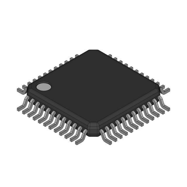
Package: 48-Pin Thin-Quad Flat Pack (TQFP)
2 Applications
•
•
•
•
•
Cellular Base Transceiver Station Transmit
Channel
– CDMA: W-CDMA, CDMA2000, IS-95
– TDMA: GSM, IS-136, EDGE/UWC-136
Medical/Test Instrumentation
Arbitrary Waveform Generators (ARB)
Direct Digital Synthesis (DDS)
Cable Modem Termination System (CMTS)
3 Description
The DAC5652 is a monolithic, dual-channel, 10-bit,
high-speed DAC with on-chip voltage reference.
Operating with update rates of up to 275 MSPS, the
DAC5652 offers exceptional dynamic performance,
tight-gain, and offset matching characteristics that
make it suitable in either I/Q baseband or direct IF
communication applications.
Each DAC has a high-impedance, differential-current
output, suitable for single-ended or differential analogoutput configurations. External resistors allow scaling
of the full-scale output current for each DAC
separately or together, typically between 2 mA and 20
mA. An accurate on-chip voltage reference is
temperature-compensated and delivers a stable 1.2-V
reference voltage. Optionally, an external reference
may be used.
The DAC5652 has two, 10-bit, parallel input ports with
separate clocks and data latches. For flexibility, the
DAC5652 also supports multiplexed data for each
DAC on one port when operating in the interleaved
mode.
The DAC5652 has been specifically designed for a
differential transformer-coupled output with a 50-Ω
doubly-terminated load. For a 20-mA full-scale output
current, both a 4:1 impedance ratio (resulting in an
output power of 4 dBm) and 1:1 impedance ratio
transformer (–2 dBm output power) are supported.
The DAC5652 is available in a 48-pin TQFP package.
Pin compatibility between family members provides
10-bit (DAC5652), 12-bit (DAC5662), and 14-bit
(DAC5672) resolution. Furthermore, the DAC5652 is
pin compatible to the DAC2900 and AD9763 dual
DACs. The device is characterized for operation over
the industrial temperature range of –40°C to 85°C.
Device Information
PART NUMBER
PACKAGE(1)
BODY SIZE (NOM)
DAC5652
TQFP
7.00 mm x 7.00 mm
(1)
For all available packages, see the orderable addendum at
the end of the data sheet.
WRTB
WRTA
CLKB
CLKA
DEMUX
IOUTA1
Latch A
10−b DAC
IOUTA2
DA[9:0]
BIASJ_A
IOUTB1
Latch B
DB[9:0]
10−b DAC
IOUTB2
MODE
BIASJ_B
GSET
1.2 V Reference
EXTIO
SLEEP
DVDD
DGND
AVDD
AGND
Functional Block Diagram
An©IMPORTANT
NOTICEIncorporated
at the end of this data sheet addresses availability, warranty, changes, use in
safety-critical
applications,
Copyright
2021 Texas Instruments
Submit
Document
Feedback
intellectual property matters and other important disclaimers. PRODUCTION DATA.
Product Folder Links: DAC5652
1
�DAC5652
www.ti.com
SLAS452E – OCTOBER 2020 – REVISED JANUARY 2021
Table of Contents
1 Features............................................................................1
2 Applications..................................................................... 1
3 Description.......................................................................1
4 Revision History.............................................................. 2
5 Pin Configuration and Functions...................................3
6 Specifications.................................................................. 4
6.1 Absolute Maximum Rationgs...................................... 4
6.2 ESD Ratings............................................................... 4
6.3 Recommended Operating Conditions.........................4
6.4 Thermal Resistance Characteristics........................... 4
6.5 Electrical Characteristics.............................................5
6.6 Electrical Characteristics.............................................6
6.7 Electrical Characteristics, AC......................................7
6.8 Electrical Characteristics, DC..................................... 8
6.9 Switching Characteristics............................................8
6.10 Typical Characteristics.............................................. 9
7 Parameter Measurement Information.......................... 12
7.1 Digital Inputs and Timing...........................................12
8 Detailed Description......................................................15
8.1 Overview................................................................... 15
8.2 Functional Block Diagram......................................... 15
8.3 Feature Description...................................................16
8.4 Device Functional Modes..........................................20
9 Application Information Disclaimer............................. 21
9.1 Application Informmation.......................................... 21
9.2 Typical Application.................................................... 21
10 Power Supply Recommendations..............................23
11 Layout........................................................................... 24
11.1 Layout Guidelines................................................... 24
11.2 Layout Example...................................................... 24
12 Device and Documentation Support..........................28
12.1 Documentation Support.......................................... 28
12.2 Receiving Notification of Documentation Updates..28
12.3 Support Resources................................................. 28
12.4 Trademarks............................................................. 28
12.5 Electrostatic Discharge Caution..............................28
12.6 Glossary..................................................................28
13 Mechanical, Packaging, and Orderable
Information.................................................................... 29
4 Revision History
NOTE: Page numbers for previous revisions may differ from page numbers in the current version.
Changes from Revision D (October 2020) to Revision E (January 2021)
Page
• Chhaged the Functional Block Diagram to inprove image quality...................................................................... 1
Changes from Revision C (Decmeber 2010) to Revision D (October 2020)
Page
• Added Device Information table, ESD Ratings table, Thermal Resistance Characteristics table, Feature
Description section, Device Functional Modes, Application and Implementation section, Power Supply
Recommendations section, Layout section, Device and Documentation Support section, and Mechanical,
Packaging, and Orderable Information section...................................................................................................1
• Changed Figure 7-1 and Figure 7-2 by removing extra wire connecting the gates of the CMOS inverter to the
output node.......................................................................................................................................................12
Changes from Revision B (March 2005) to Revision C (December 2010)
Page
• Changed the non-printing µ symbols in the Digital Input section of the Electrical Characteristics table (Units
column) to the correct µ symbols recognized by the PDF processor..................................................................8
2
Submit Document Feedback
Copyright © 2021 Texas Instruments Incorporated
Product Folder Links: DAC5652
�DAC5652
www.ti.com
SLAS452E – OCTOBER 2020 – REVISED JANUARY 2021
MODE
AVDD
IOUTA1
IOUTA2
BIASJ_A
EXTIO
GSET
BIASJ_B
IOUTB2
IOUTB1
AGND
SLEEP
5 Pin Configuration and Functions
1
48 47 46 45 44 43 42 41 40 39 38 37
36
2
35
3
34
33
4
5
Top View
48-Pin TQFP
PFB Package
6
7
32
31
30
8
29
9
28
10
27
11
26
25
12
13 14 15 16 17 18 19 20 21 22 23 24
NC
NC
NC
NC
DB0 (LSB)
DB1
DB2
DB3
DB4
DB5
DB6
DB7
NC
NC
DGND
DVDD
WRTA/WRTIQ
CLKA/CLKIQ
CLKB/RESETIQ
WRTB/SELECTIQ
DGND
DVDD
DB9 (MSB)
DB8
DA9 (MSB)
DA8
DA7
DA6
DA5
DA4
DA3
DA2
DA1
DA0 (LSB)
NC
NC
Table 5-1. Pin Functions
PIN
I/O
DESCRIPTION
NAME
NO.
AGND
38
I
Analog ground
AVDD
47
I
Analog supply voltage
BIASJ_A
44
O
Full-scale output current bias for DACA
BIASJ_B
41
O
Full-scale output current bias for DACB
CLKA/CLKIQ
18
I
Clock input for DACA, CLKIQ in interleaved mode
CLKB/RESETIQ
19
I
Clock input for DACB, RESETIQ in interleaved mode
DA[9:0]
1-10
I
Data port A. DA9 is MSB and DA0 is LSB. Internal pulldown.
DB[9:0]
23-32
I
Data port B. DB9 is MSB and DB0 is LSB. Internal pulldown.
DGND
15, 21
I
Digital ground
DVDD
16, 22
I
Digital supply voltage
EXTIO
43
I/O
GSET
42
I
Gain-setting mode: H – 1 resistor, L – 2 resistors. Internal pullup.
IOUTA1
46
O
DACA current output. Full-scale with all bits of DA high.
IOUTA2
45
O
DACA complementary current output. Full-scale with all bits of DA low.
IOUTB1
39
O
DACB current output. Full-scale with all bits of DB high.
IOUTB2
40
O
DACB complementary current output. Full-scale with all bits of DB low.
MODE
Internal reference output (bypass with 0.1 μF to AGND) or external reference input
48
I
Mode Select: H – Dual Bus, L – Interleaved. Internal pullup.
11-14, 33-36
-
Factory use only. Pins must be connected to DGND or left unconnected.
SLEEP
37
I
Sleep function control input: H – DAC in power-down mode, L – DAC in operating mode.
Internal pulldown.
WRTA/WRTIQ
17
I
Input write signal for PORT A (WRTIQ in interleaving mode)
WRTB/SELECTIQ
20
I
Input write signal for PORT B (SELECTIQ in interleaving mode)
NC
Submit Document Feedback
Copyright © 2021 Texas Instruments Incorporated
Product Folder Links: DAC5652
3
�DAC5652
www.ti.com
SLAS452E – OCTOBER 2020 – REVISED JANUARY 2021
6 Specifications
6.1 Absolute Maximum Rationgs
over TA (unless otherwise noted)(1)
AVDD(2)
Supply voltage range
DVDD(3)
Voltage between AGND and DGND
Voltage between AVDD and DVDD
Supply voltage range
Min
Max
–0.5
4
UNIT
V
–0.5
4
V
–0.5
0.5
V
–0.5
0.5
V
DA[9:0] and DB[9:0](3)
–0.5
DVDD + 0.5
V
MODE, SLEEP, CLKA, CLKB, WRTA,
WRTB(3)
–0.5
DVDD + 0.5
IOUTA1, IOUTA2, IOUTB1, IOUTB2(2) –1
EXTIO, BIASJ_A, BIASJ_B,
GSET(2)
V
AVDD + 0.5
–0.5
V
AVDD + 0.5
Peak input current (any input)
Peak total input current (all inputs)
V
+20
mA
–30
mA
Operating free-air temperature range
–40
85
°C
Storage temperature range
–65
150
°C
(1)
(2)
(3)
Stresses beyond those listed under “absolute maximum ratings” may cause permanent damage to the device. These are stress ratings
only and functional operation of these or any other conditions beyond those indicated under “recommended operating conditions” is not
implied. Exposure to absolute-maximum-rated conditions for extended periods may affect device reliability.
Measured with respect to AGND.
Measured with respect to DGND.
6.2 ESD Ratings
VALUE
V (ESD)
Electrostatic discharge
Human-body model (HBM), per ANSI/ESDA/JEDEC
JS-0011
±2000
Charged-device model (CDM), per JEDEC specification JESD22-C1012
±1000
UNIT
V
over operating free-air temperature range (unless otherwise noted)
6.3 Recommended Operating Conditions
AVDD
Analog supply voltage
DVDD
Digital supply voltage
Output voltage compliance range(1)
MIN
NOM
MAX
3
3.3
3.6
V
3
3.3
-1
Clock input frequency
TA
Operating free-air temperature
-40
UNIT
3.6
V
1.25
V
275
MHz
85
°C
1. The lower limit of the output compliance is determined by the CMOS process. Exceeding this limit may result
in transistor breakdown, resulting in reduced reliability of the DAC5652 device. The upper limit of the output
compliance is determined by the load resistors and full-scale output current. Exceeding the upper limit
adversely affects distortion performance and integral nonlinearity.
6.4 Thermal Resistance Characteristics
DAC5652
THERMAL METRIC(1)
TQFP (PFB)
UNIT
48-Pins
4
R θJA
Junction-to-ambient thermal resistance
65.3
°C/W
R θJC(top)
Junction-to-case (top) thermal resistance
16.4
°C/W
Submit Document Feedback
Copyright © 2021 Texas Instruments Incorporated
Product Folder Links: DAC5652
�DAC5652
www.ti.com
SLAS452E – OCTOBER 2020 – REVISED JANUARY 2021
6.4 Thermal Resistance Characteristics (continued)
DAC5652
THERMAL
METRIC(1)
TQFP (PFB)
UNIT
48-Pins
R θJB
Junction-to-board thermal resistance
28.6
°C/W
ψ JT
Junction-to-top characterization parameter
0.4
°C/W
ψ JB
Junction-to-board characterization parameter
28.4
°C/W
R θJC(bot)
Junction-to-case (bottom) thermal resistance
n/a
°C/W
(1)
For more information about traditional and new thermal metrics, see the Semiconductor and IC package thermal metrics application
report.
6.5 Electrical Characteristics
over TA, AVDD = DVDD = 3.3 V, IOUTFS = 20 mA, independent gain set mode (unless otherwise noted)
PARAMETER
TEST CONDITIONS
MIN
TYP
MAX
UNIT
DC Specifications
Resolution
DC
10
Bits
Accuracy(1)
INL
Integral nonlinearity
DNL
Differential nonlinearity
1 LSB = IOUTFS/210, TMIN to TMAX
–1
±0.25
1
LSB
–0.5
±0.16
0.5
LSB
Analog Output
Offset error
Midscale value (internal reference)
±0.05
%FSR
Offset mismatch
Midscale value (internal reference)
±0.03
%FSR
Gain error
With internal reference
±0.75
%FSR
current(2)
2
mA
Maximum full-scale output current(2)
20
mA
Minimum full-scale output
Gain mismatch
With internal reference
Output voltage compliance range(3)
RO
Output resistance
CO
Output capacitance
–2
0.2
–1
2
1.25
%FSR
V
300
kΩ
5
pF
Reference Output
Reference voltage
Reference output
1.14
current(4)
1.2
1.26
100
V
nA
Reference Input
VEXTIO
Input voltage
RI
Input resistance
CI
0.1
1.25
V
1
MΩ
Small signal bandwidth
300
kHz
Input capacitance
100
pF
Temperature Coefficients
2
ppm of
FSR/°C
With external reference
±20
ppm of
FSR/°C
With internal reference
±40
ppm of
FSR/°C
±20
ppm/°C
Offset drift
Gain drift
Reference voltage drift
(1)
(2)
Measured differentially through 50 Ω to AGND.
Nominal full-scale current, IOUTFS, equals 32x the IBIAS current.
Submit Document Feedback
Copyright © 2021 Texas Instruments Incorporated
Product Folder Links: DAC5652
5
�DAC5652
www.ti.com
SLAS452E – OCTOBER 2020 – REVISED JANUARY 2021
(3)
(4)
The lower limit of the output compliance is determined by the CMOS process. Exceeding this limit may result in transistor breakdown,
resulting in reduced reliability of the DAC5652 device. The upper limit of the output compliance is determined by the load resistors and
full-scale output current. Exceeding the upper limit adversely affects distortion performance and integral nonlinearity.
Use an external buffer amplifier with high-impedance input to drive any external load.
6.6 Electrical Characteristics
over TA, AVDD = DVDD = 3.3 V, IOUTFS = 20 mA, fDATA = 200 MSPS, fOUT = 1 MHz, independent gain set mode (unless
otherwise noted)
PARAMETER
TEST CONDITIONS
MIN
TYP
MAX
UNIT
Power Supply
AVDD
Analog supply voltage
3
3.3
3.6
V
DVDD
Digital supply voltage
3
3.3
3.6
V
Including output current through load
resistor
75
90
Sleep mode with clock
2.5
Sleep mode without clock
2.5
IAVDD
Supply current, analog
IDVDD
Supply current, digital
Sleep mode with clock
Sleep mode without clock
12
20
11.3
18
6
mA
0.6
290
Power dissipation
mA
Sleep mode with clock
360
45.5
Sleep mode without clock
9.2
fDATA = 275 MSPS, fOUT = 20 MHz
310
mW
APSRR
Analog power supply rejection ratio
–0.2
–0.01
0.2
%FSR/V
DPSRR
Digital power supply rejection ratio
–0.2
0
0.2
%FSR/V
TA
Operating free-air temperature
–40
85
°C
Submit Document Feedback
Copyright © 2021 Texas Instruments Incorporated
Product Folder Links: DAC5652
�DAC5652
www.ti.com
SLAS452E – OCTOBER 2020 – REVISED JANUARY 2021
6.7 Electrical Characteristics, AC
AC specifications over TA, AVDD = DVDD = 3.3 V, IOUTFS = 20 mA, independent gain set mode, differential 1:1 impedance
ratio transformer coupled output, 50-Ω doubly terminated load (unless otherwise noted)
PARAMETER
TEST CONDITIONS
MIN
TYP
MAX
UNIT
Analog Output
fclk
Maximum output update
rate(1)
ts
Output settling time to 0.1%
(DAC)
tr
tf
275
20
ns
Output rise time 10% to 90%
(OUT)
1.4
ns
Output fall time 90% to 10%
(OUT)
1.5
ns
Output noise
Mid-scale transition
MSPS
IOUTFS = 20 mA
55
IOUTFS = 2 mA
30
1st Nyquist zone, TA = 25°C,
fDATA = 50 MSPS, fOUT = 1 MHz, IOUTFS = 0 dB
79
1st Nyquist zone, TA = 25°C,
fDATA = 50 MSPS, fOUT = 1 MHz, IOUTFS = –6 dB
78
1st Nyquist zone, TA = 25°C,
fDATA = 50 MSPS, fOUT = 1 MHz, IOUTFS = –12 dB
73
1st Nyquist zone, TA = 25°C,
fDATA = 100 MSPS, fOUT = 5 MHz, IOUTFS = 0 dB
80
1st Nyquist zone, TA = 25°C,
fDATA = 100 MSPS, fOUT = 20 MHz, IOUTFS = 0 dB
76
pA/√Hz
AC Linearity
SFDR
Spurious-free dynamic range
1st Nyquist zone, TMIN to TMAX,
fDATA = 200 MSPS, fOUT = 20 MHz, IOUTFS = 0 dB
SNR
Signal-to-noise ratio
IMD3
IMD
Third-order two-tone
intermodulation
Four-tone intermodulation
Channel isolation
(1)
dBc
61
70
1st Nyquist zone, TA = 25°C,
fDATA = 200 MSPS, fOUT = 41 MHz, IOUTFS = 0 dB
67
1st Nyquist zone, TA = 25°C,
fDATA = 275 MSPS, fOUT = 20 MHz
70
1st Nyquist zone, TA = 25°C,
fDATA = 100 MSPS, fOUT = 5 MHz, IOUTFS = 0 dB
63
dB
1st Nyquist zone, TA = 25°C,
fDATA = 160 MSPS, fOUT = 20 MHz, IOUTFS = 0 dB
62
dB
Each tone at –6 dBFS, TA = 25°C,
fDATA = 200 MSPS, fOUT = 45.4 MHz and 46.4 MHz
61
Each tone at –6 dBFS, TA = 25°C,
fDATA = 100 MSPS, fOUT = 15.1 MHz and 16.1 MHz
78
Each tone at –12 dBFS, TA = 25°C
fDATA = 100 MSPS, fOUT = 15.6, 15.8, 16.2, and
16.4 MHz
76
Each tone at –12 dBFS, TA = 25°C
fDATA = 165 MSPS, fOUT = 19.0, 19.1, 19.3, and
19.4 MHz
55
Each tone at –12 dBFS, TA = 25°C
fDATA = 165 MSPS, fOUT = 68.8, 69.6, 71.2, and
72.0 MHz
70
TA = 25°C, fDATA = 165 MSPS
fOUT (CH1) = 20 MHz, fOUT (CH2) = 21 MHz
90
dBc
dBc
dBc
Specified by design and bench characterization. Not production tested.
Submit Document Feedback
Copyright © 2021 Texas Instruments Incorporated
Product Folder Links: DAC5652
7
�DAC5652
www.ti.com
SLAS452E – OCTOBER 2020 – REVISED JANUARY 2021
6.8 Electrical Characteristics, DC
Digital specifications over TA, AVDD = DVDD = 3.3 V, IOUTFS = 20 mA (unless otherwise noted)
PARAMETER
TEST CONDITIONS
MIN
TYP
MAX
UNIT
Digital Input
VIH
High-level input voltage
2
0
3.3
0.8
V
VIL
Low-level input voltage
IIH
High-level input current
±50
µA
V
IIL
Low-level input current
±10
µA
IIH(GSET)
High-level input current, GSET pin
7
µA
IIL(GSET)
Low-level input current, GSET pin
–80
µA
IIH(MODE)
High-level input current, MODE pin
–30
µA
IIL(MODE)
Low-level input current, MODE pin
–80
µA
CI
Input capacitance
5
pF
6.9 Switching Characteristics
Digital specifications over TA, AVDD = DVDD = 3.3 V, IOUTFS = 20 mA (unless otherwise noted)
PARAMETER
TEST CONDITIONS
MIN
TYP
MAX
UNIT
Timing - Dual Bus Mode
tsu
Input setup time
1
ns
th
Input hold time
1
ns
tLPH
Input clock pulse high time
tLAT
Clock latency (WRTA/B to outputs)
tPD
Propagation delay time
1
4
ns
4
clk
1.5
ns
Timing - Single Bus Interleaved Mode
8
tsu
Input setup time
0.5
ns
th
Input hold time
0.5
ns
tLAT
Clock latency (WRTA/B to outputs)
tPD
Propagation delay time
4
4
1.5
Submit Document Feedback
clk
ns
Copyright © 2021 Texas Instruments Incorporated
Product Folder Links: DAC5652
�DAC5652
www.ti.com
SLAS452E – OCTOBER 2020 – REVISED JANUARY 2021
INL − Integral Nonlinearity Error − LSB
6.10 Typical Characteristics
0.5
0.4
0.3
0.2
0.1
0.0
−0.1
−0.2
−0.3
−0.4
−0.5
0
100
200
300
400
500
600
700
800
900
1000
Input Code
G001
DNL − Differential Nonlinearity Error − LSB
Figure 6-1. Integral Nonlinearity vs Input Code
0.25
0.20
0.15
0.10
0.05
0.00
−0.05
−0.10
−0.15
−0.20
−0.25
0
100
200
300
400
500
600
700
800
900
1000
Input Code
G002
Figure 6-2. Differential Nonlinearity vs Input Code
100
SFDR − Spurious-Free Dynamic Range − dBc
SFDR − Spurious-Free Dynamic Range − dBc
100
fdata = 52 MSPS
Dual Bus Mode
95
90
85
−6 dBfS
0 dBfS
80
75
−12 dBfS
70
65
60
fdata = 78 MSPS
Dual Bus Mode
95
90
85
−6 dBfS
80
75
−12 dBfS
70
0 dBfS
65
60
0
4
8
12
16
fout − Output Frequency − MHz
20
0
10
15
20
fout − Output Frequency − MHz
G003
Figure 6-3. Spurious-Free Dynamic Range vs
Output Frequency
5
25
30
G004
Figure 6-4. Spurious-Free Dynamic Range vs
Output Frequency
Submit Document Feedback
Copyright © 2021 Texas Instruments Incorporated
Product Folder Links: DAC5652
9
�DAC5652
www.ti.com
SLAS452E – OCTOBER 2020 – REVISED JANUARY 2021
100
SFDR − Spurious-Free Dynamic Range − dBc
SFDR − Spurious-Free Dynamic Range − dBc
100
fdata = 100 MSPS
Dual Bus Mode
95
90
85
−6 dBfS
80
0 dBfS
75
−12 dBfS
70
65
60
fdata = 165 MSPS
Dual Bus Mode
95
90
85
80
0 dBfS
−6 dBfS
75
70
−12 dBfS
65
60
0
5
10
15
20
25
30
fout − Output Frequency − MHz
35
0
10 15 20 25 30 35 40 45 50 55 60
fout − Output Frequency − MHz
G005
Figure 6-5. Spurious-Free Dynamic Range vs
Output Frequency
5
0
0
fdata = 78 MSPS
fOUT = 15 MHz
Dual Bus Mode
fdata = 165 MSPS
fOUT = 30.1 MHz
Dual Bus Mode
−20
Power − dBm
−20
Power − dBm
G006
Figure 6-6. Spurious-Free Dynamic Range vs
Output Frequency
−40
−60
−80
−40
−60
−80
−100
0.0
7.8
15.6
23.4
31.2
−100
0.0
39.0
16.5
f − Frequency − MHz
33.0
49.5
66.0
82.5
f − Frequency − MHz
G007
G008
Figure 6-7. Single-Tone Spectrum
Figure 6-8. Single-Tone Spectrum
95
100
95
90
Two-Tone IMD3 − dBc
Two-Tone IMD3 − dBc
90
85
80
75
70
85
80
75
70
65
60
fdata = 78 MSPS
Dual Bus Mode
fout2 = fout1 + 1 MHz
65
60
50
0
5
10
15
20
25
fout1 − Output Frequency − MHz
30
35
0
10
20
30
40
fout1 − Output Frequency − MHz
G009
Figure 6-9. Two-Tone IMD3 vs Output Frequency
10
fdata = 165 MSPS
Dual Bus Mode
fout2 = fout1 + 1 MHz
55
50
G010
Figure 6-10. Two-Tone IMD3 vs Output Frequency
Submit Document Feedback
Copyright © 2021 Texas Instruments Incorporated
Product Folder Links: DAC5652
�DAC5652
www.ti.com
SLAS452E – OCTOBER 2020 – REVISED JANUARY 2021
−10
fdata = 165 MSPS
fdata = 78 MSPS
fout1 = 20.1 MHz
fout2 = 21.1 MHz
Dual Bus Mode
−10 fout1 = 30.1 MHz
fout2 = 31.1 MHz
Dual Bus Mode
−30
Power − dBm
Power − dBm
−30
−50
−70
−90
−110
19.0
−50
−70
−90
19.5
20.0
20.5
21.0
21.5
−110
29.0
22.0
f − Frequency − MHz
29.5
30.0
30.5
31.0
31.5
32.0
f − Frequency − MHz
G011
Figure 6-11. Two-Tone Spectrum
G012
Figure 6-12. Two-Tone Spectrum
Submit Document Feedback
Copyright © 2021 Texas Instruments Incorporated
Product Folder Links: DAC5652
11
�DAC5652
www.ti.com
SLAS452E – OCTOBER 2020 – REVISED JANUARY 2021
7 Parameter Measurement Information
7.1 Digital Inputs and Timing
7.1.1 Digital Inputs
The data input ports of the DAC5652 accept a standard positive coding with data bits DA9 and DB9 being the
most significant bits (MSB). The converter outputs support a clock rate of up to 275 MSPS. The best
performance is typically achieved with a symmetric duty cycle for write and clock; however, the duty cycle may
vary as long as the timing specifications are met. Similarly, the setup and hold times may be chosen within their
specified limits.
All digital inputs of the DAC5652 are CMOS compatible. Figure 7-1 and Figure 7-2 show schematics of the
equivalent CMOS digital inputs of the DAC5652. The pullup and pulldown circuitry is approximately equivalent to
100kΩ.The 10-bit digital data input follows the offset positive binary coding scheme. The DAC5652 is designed
to operate with a digital supply (DVDD) of 3 V to 3.6 V.
DVDD
DA[9:0]
DB[9:0]
SLEEP
CLKA/B
WRTA/B
400W
Internal
Digital In
100kW
DGND
Figure 7-1. CMOS/TTL Digital Equivalent Input With Internal Pulldown Resistor
DVDD
100kW
GSET
MODE
400W
Internal
Digital In
DGND
Figure 7-2. CMOS/TTL Digital Equivalent Input With Internal Pullup Resistor
12
Submit Document Feedback
Copyright © 2021 Texas Instruments Incorporated
Product Folder Links: DAC5652
�DAC5652
www.ti.com
SLAS452E – OCTOBER 2020 – REVISED JANUARY 2021
7.1.2 Input Interfaces
The DAC5652 features two operating modes selected by the MODE pin, as shown in Table 7-1.
•
•
For dual-bus input mode, the device essentially consists of two separate DACs. Each DAC has its own
separate data input bus, clock input, and data write signal (data latch-in).
In single-bus interleaved mode, the data must be presented interleaved at the A-channel input bus. The Bchannel input bus is not used in this mode. The clock and write input are now shared by both DACs.
Table 7-1. Operating Modes
MODE Pin
MODE pin connected to DGND
MODE pin connected to DVDD
Bus input
Single-bus interleaved mode, clock and write input equal for both DACs
Dual-bus mode, DACs operate independently
7.1.3 Dual-Bus Data Interface and Timing
In dual-bus mode, the MODE pin is connected to DVDD. The two converter channels within the DAC5652
consist of two independent, 10-bit, parallel data ports. Each DAC channel is controlled by its own set of write
(WRTA, WRTB) and clock (CLKA, CLKB) lines. The WRTA/B lines control the channel input latches and the
CLKA/B lines control the DAC latches. The data is first loaded into the input latch by a rising edge of the
WRTA/B line.
The internal data transfer requires a correct sequence of write and clock inputs, since essentially two clock
domains having equal periods (but possibly different phases) are input to the DAC5652. This is defined by a
minimum requirement of the time between the rising edge of the clock and the rising edge of the write inputs.
This essentially implies that the rising edge of CLKA/B must occur at the same time or before the rising edge of
the WRTA/B signal. A minimum delay of 2 ns must be maintained if the rising edge of the clock occurs after the
rising edge of the write. Note that these conditions are satisfied when the clock and write inputs are connected
externally. Note that all specifications were measured with the WRTA/B and CLKA/B lines connected together.
DA[9:0]/DB[9:0]
Valid Data
tsu
th
tLPH
WRTA/WRTB
CLKA/CLKB
ts
tPD
tLAT
IOUT
or
IOUT
Figure 7-3. Dual-Bus Mode Operation
Submit Document Feedback
Copyright © 2021 Texas Instruments Incorporated
Product Folder Links: DAC5652
13
�DAC5652
www.ti.com
SLAS452E – OCTOBER 2020 – REVISED JANUARY 2021
7.1.4 Single-Bus Interleaved Data Interface and Timing
In single-bus interleaved mode, the MODE pin is connected to DGND. Figure 7-4 shows the timing diagram. In
interleaved mode, the A- and B-channels share the write input (WRTIQ) and update clock (CLKIQ and internal
CLKDACIQ). Multiplexing logic directs the input word at the A-channel input bus to either the A-channel input
latch (SELECTIQ is high) or to the B-channel input latch (SELECTIQ is low). When SELECTIQ is high, the data
value in the B-channel latch is retained by presenting the latch output data to its input again. When SELECTIQ is
low, the data value in the A-channel latch is retained by presenting the latch output data to its input.
In interleaved mode, the A-channel input data rate is twice the update rate of the DAC core. As in dual-bus
mode, it is important to maintain a correct sequence of write and clock inputs. The edge-triggered flip-flops latch
the A- and B-channel input words on the rising edge of the write input (WRTIQ). This data is presented to the Aand B-DAC latches on the following falling edge of the write inputs. The DAC5652 clock input is divided by a
factor of two before it is presented to the DAC latches.
Correct pairing of the A- and B-channel data is done by RESETIQ. In interleaved mode, the clock input CLKIQ is
divided by two, which would translate to a non-deterministic relation between the rising edges of the CLKIQ and
CLKDACIQ. RESETIQ ensures, however, that the correct position of the rising edge of CLKDACIQ with respect
to the data at the input of the DAC latch is determined. CLKDACIQ is disabled (low) when RESETIQ is high.
DA[9:0]
Valid Data
tsu
th
SELECTIQ
WRTIQ
CLKIQ
RESETIQ
ts
tPD
tLAT
IOUT
or
IOUT
Figure 7-4. Single-Bus Interleaved Mode Operation
14
Submit Document Feedback
Copyright © 2021 Texas Instruments Incorporated
Product Folder Links: DAC5652
�DAC5652
www.ti.com
SLAS452E – OCTOBER 2020 – REVISED JANUARY 2021
8 Detailed Description
8.1 Overview
The architecture of the DAC5652 uses a current steering technique to enable fast switching and high update
rate. The core element within the monolithic DAC is an array of segmented current sources that are designed to
deliver a full-scale output current of up to 20 mA. An internal decoder addresses the differential current switches
each time the DAC is updated and a corresponding output current is formed by steering all currents to either
output summing node, IOUT1 or IOUT2. The complementary outputs deliver a differential output signal, which
improves the dynamic performance through reduction of even-order harmonics, common-mode signals (noise),
and double the peak-to-peak output signal swing by a factor of two, as compared to single-ended operation.
The segmented architecture results in a significant reduction of the glitch energy and improves the dynamic
performance (SFDR) and DNL. The current outputs maintain a very high output impedance of greater
than 300 kΩ.
When pin 42 (GSET) is high (simultaneous gain set mode), the full-scale output current for both DACs is
determined by the ratio of the internal reference voltage (1.2 V) and an external resistor (RSET) connected to
BIASJ_A. When GSET is low (independent gain set mode), the full-scale output current for each DAC is
determined by the ratio of the internal reference voltage (1.2 V) and separate external resistors (RSET)
connected to BIASJ_A and BIASJ_B. The resulting IREF is internally multiplied by a factor of 32 to produce an
effective DAC output current that can range from 2 mA to 20 mA, depending on the value of RSET.
The DAC5652 is split into a digital and an analog portion, each of which is powered through its own supply pin.
The digital section includes edge-triggered input latches and the decoder logic, while the analog section
comprises both the current source array with its associated switches, and the reference circuitry.
8.2 Functional Block Diagram
WRTB
WRTA
CLKB
CLKA
DEMUX
IOUTA1
Latch A
10−b DAC
IOUTA2
DA[9:0]
BIASJ_A
IOUTB1
Latch B
DB[9:0]
10−b DAC
IOUTB2
MODE
BIASJ_B
GSET
1.2 V Reference
EXTIO
SLEEP
DVDD
DGND
AVDD
AGND
Submit Document Feedback
Copyright © 2021 Texas Instruments Incorporated
Product Folder Links: DAC5652
15
�DAC5652
www.ti.com
SLAS452E – OCTOBER 2020 – REVISED JANUARY 2021
8.3 Feature Description
8.3.1 DAC Transfer Function
Each of the DACs in the DAC5652 has a set of complementary current outputs, IOUT1 and IOUT2. The full-scale
output current, IOUTFS, is the summation of the two complementary output currents:
I
OUTFS
+I
OUT1
)I
OUT2
(1)
The individual output currents depend on the DAC code and can be expressed as:
I
I
OUT1
+I
OUTFS
Ǔ
ǒCode
1024
(2)
OUT2
+I
OUTFS
* CodeǓ
ǒ10231024
(3)
where Code is the decimal representation of the DAC data input word. Additionally, IOUTFS is a function of the
reference current IREF, which is determined by the reference voltage and the external setting resistor (RSET).
V
I
OUTFS
+ 32
I
REF
+ 32
REF
R
SET
(4)
In most cases, the complementary outputs drive resistive loads or a terminated transformer. A signal voltage
develops at each output according to:
V
V
OUT1
+I
OUT1
OUT2
+I
OUT2
R
R
LOAD
(5)
LOAD
(6)
The value of the load resistance is limited by the output compliance specification of the DAC5652. To maintain
specified linearity performance, the voltage for IOUT1 and IOUT2 must not exceed the maximum allowable
compliance range.
The total differential output voltage is:
V
V
16
OUTDIFF
+V
OUTDIFF
+
OUT1
(2
*V
OUT2
Code * 1023)
1024
(7)
I
OUTFS
R
LOAD
Submit Document Feedback
(8)
Copyright © 2021 Texas Instruments Incorporated
Product Folder Links: DAC5652
�DAC5652
www.ti.com
SLAS452E – OCTOBER 2020 – REVISED JANUARY 2021
8.3.2 Analog Outputs
The DAC5652 provides two complementary current outputs, IOUT1 and IOUT2. The simplified circuit of the analog
output stage representing the differential topology is shown in Figure 8-1. The output impedance of IOUT1 and
IOUT2 results from the parallel combination of the differential switches, along with the current sources and
associated parasitic capacitances.
AVDD
S(1)
IOUT1
RLOAD
S(1)C
IOUT2
S(2)
S(2)C
S(N)
S(N)C
Current Source Array
RLOAD
Figure 8-1. Analog Outputs
The signal voltage swing that may develop at the two outputs, IOUT1 and IOUT2, is limited by a negative and
positive compliance. The negative limit of –1 V is given by the breakdown voltage of the CMOS process and
exceeding it compromises the reliability of the DAC5652 (or even causes permanent damage). With the fullscale output set to 20 mA, the positive compliance equals 1.2 V. Note that the compliance range decreases to
about
1 V for a selected output current of IOUTFS = 2 mA. Care must be taken that the configuration of DAC5652 does
not exceed the compliance range to avoid degradation of the distortion performance and integral linearity.
Best distortion performance is typically achieved with the maximum full-scale output signal limited to
approximately 0.5 VPP. This is the case for a 50-Ω doubly-terminated load and a 20-mA full-scale output current.
A variety of loads can be adapted to the output of the DAC5652 by selecting a suitable transformer while
maintaining optimum voltage levels at IOUT1 and I OUT2. Furthermore, using the differential output configuration in
combination with a transformer is instrumental for achieving excellent distortion performance. Common-mode
errors, such as even-order harmonics or noise, can be substantially reduced. This is particularly the case with
high output frequencies.
For those applications requiring the optimum distortion and noise performance, it is recommended to select a
full-scale output of 20 mA. A lower full-scale range of 2 mA may be considered for applications that require low
power consumption, but can tolerate a slight reduction in performance level.
8.3.3 Output Configurations
The current outputs of the DAC5652 allow for a variety of configurations. As mentioned previously, utilizing the
converter’s differential outputs yield the best dynamic performance. Such a differential output circuit may consist
of an RF transformer or a differential amplifier configuration. The transformer configuration is ideal for most
applications with ac coupling, while op amps are suitable for a dc-coupled configuration.
The single-ended configuration may be considered for applications requiring a unipolar output voltage.
Connecting a resistor from either one of the outputs to ground converts the output current into a groundreferenced voltage signal. To improve on the dc linearity by maintaining a virtual ground, an I-to-V or op-amp
configuration may be considered.
Submit Document Feedback
Copyright © 2021 Texas Instruments Incorporated
Product Folder Links: DAC5652
17
�DAC5652
www.ti.com
SLAS452E – OCTOBER 2020 – REVISED JANUARY 2021
8.3.4 Differential With Transformer
Using an RF transformer provides a convenient way of converting the differential output signal into a singleended signal while achieving excellent dynamic performance. The appropriate transformer must be carefully
selected based on the output frequency spectrum and impedance requirements.
The differential transformer configuration has the benefit of significantly reducing common-mode signals, thus
improving the dynamic performance over a wide range of frequencies. Furthermore, by selecting a suitable
impedance ratio (winding ratio) the transformer can provide optimum impedance matching while controlling the
compliance voltage for the converter outputs.
Figure 8-2 and Figure 8-3 show 50-Ω doubly-terminated transformer configurations with 1:1 and 4:1 impedance
ratios, respectively. Note that the center tap of the primary input of the transformer has to be grounded to enable
a dc-current flow. Applying a 20-mA full-scale output current would lead to a 0.5-VPP output for a 1:1 transformer
and a 1-VPP output for a 4:1 transformer. In general, the 1:1 transformer configuration will have slightly better
output distortion, but the 4:1 transformer will have 6 dB higher output power.
50 Ω
1:1
IOUT1
RLOAD
50 Ω
AGND
100 Ω
IOUT2
50 Ω
Figure 8-2. Driving a Doubly-Terminated 50-Ω Cable Using a 1:1 Impedance Ratio Transformer
100 Ω
4:1
IOUT1
AGND
RLOAD
50 Ω
IOUT2
100 Ω
Figure 8-3. Driving a Doubly-Terminated 50-Ω Cable Using a 4:1 Impedance Ratio Transformer
8.3.5 Single-Ended Configuration
Figure 8-4 shows the single-ended output configuration, where the output current IOUT1 flows into an equivalent
load resistance of 25 Ω. Node IOUT2 must be connected to AGND or terminated with a resistor of 25 Ω to
AGND. The nominal resistor load of 25 Ω gives a differential output swing of 1 VPP when applying a 20-mA fullscale output current.
18
Submit Document Feedback
Copyright © 2021 Texas Instruments Incorporated
Product Folder Links: DAC5652
�DAC5652
www.ti.com
SLAS452E – OCTOBER 2020 – REVISED JANUARY 2021
IOUT1
RLOAD
50 Ω
IOUT2
50 Ω
25 Ω
AGND
Figure 8-4. Driving a Doubly-Terminated 50-Ω Cable Using a Single-Ended Output
8.3.6 Reference Operation
8.3.6.1 Internal Reference
The DAC5652 has an on-chip reference circuit which comprises a 1.2-V bandgap reference and two control
amplifiers, one for each DAC. The full-scale output current, IOUTFS, of the DAC5652 is determined by the
reference voltage, VREF, and the value of resistor RSET. IOUTFS can be calculated by:
V
I
OUTFS
+ 32
I
REF
+ 32
REF
R
SET
(9)
The reference control amplifier operates as a V-to-I converter producing a reference current, IREF, which is
determined by the ratio of VREF and RSET (see Equation 9). The full-scale output current, IOUTFS, results from
multiplying IREF by a fixed factor of 32.
Using the internal reference, a 2-kΩ resistor value results in a full-scale output of approximately 20 mA.
Resistors with a tolerance of 1% or better should be considered. Selecting higher values, the output current can
be adjusted from 20 mA down to 2 mA. Operating the DAC5652 at lower than 20-mA output currents may be
desirable for reasons of reducing the total power consumption, improving the distortion performance, or
observing the output compliance voltage limitations for a given load condition.
It is recommended to bypass the EXTIO pin with a ceramic chip capacitor of 0.1 µF or more. The control
amplifier is internally compensated and its small signal bandwidth is approximately 300 kHz.
8.3.6.2 External Reference
The internal reference can be disabled by simply applying an external reference voltage into the EXTIO pin,
which in this case functions as an input. The use of an external reference may be considered for applications
that require higher accuracy and drift performance or to add the ability of dynamic gain control.
While a 0.1-µF capacitor is recommended to be used with the internal reference, it is optional for the external
reference operation. The reference input, EXTIO, has a high input impedance (1 MΩ) and can easily be driven
by various sources. Note that the voltage range of the external reference must stay within the compliance range
of the reference input.
8.3.7 Gain Setting Option
The full-scale output current on the DAC5652 can be set two ways: either for each of the two DAC channels
independently or for both channels simultaneously. For the independent gain set mode, the GSET pin (pin 42)
must be low (that is, connected to AGND). In this mode, two external resistors are required — one RSET
connected to the BIASJ_A pin (pin 44) and the other to the BIASJ_B pin (pin 41). In this configuration, the user
has the flexibility to set and adjust the full-scale output current for each DAC independently, allowing for the
compensation of possible gain mismatches elsewhere within the transmit signal path.
Alternatively, bringing the GSET pin high (that is, connected to AVDD), the DAC5652 switches into the
simultaneous gain set mode. Now the full-scale output current of both DAC channels is determined by only one
Submit Document Feedback
Copyright © 2021 Texas Instruments Incorporated
Product Folder Links: DAC5652
19
�DAC5652
www.ti.com
SLAS452E – OCTOBER 2020 – REVISED JANUARY 2021
external RSET resistor connected to the BIASJ_A pin. The resistor at the BIASJ_B pin may be removed;
however, this is not required since this pin is not functional in this mode and the resistor has no effect on the gain
equation.
8.4 Device Functional Modes
8.4.1 Sleep Mode
The DAC5652 features a power-down function which can reduce the total supply current to approximately 3.1
mA over the specified supply range if no clock is present. Applying a logic high to the SLEEP pin initiates the
power-down mode, while a logic low enables normal operation. When left unconnected, an internal active
pulldown circuit enables the normal operation of the converter.
20
Submit Document Feedback
Copyright © 2021 Texas Instruments Incorporated
Product Folder Links: DAC5652
�DAC5652
www.ti.com
SLAS452E – OCTOBER 2020 – REVISED JANUARY 2021
9 Application Information Disclaimer
Note
Information in the following applications sections is not part of the TI component specification, and TI
does not warrant its accuracy or completeness. TI’s customers are responsible for determining
suitability of components for their purposes, as well as validating and testing their design
implementation to confirm system functionality.
9.1 Application Informmation
The lower limit of the output compliance is determined by the CMOS process. Exceeding this limit may result in
transistor breakdown, resulting in reduced reliability of the DAC5652 device. The upper limit of the output
compliance is determined by the load resistors and full-scale output current. Exceeding the upper limit adversely
affects distortion performance and integral nonlinearity.
9.2 Typical Application
A typical application for the DAC5652 is a dual- or single-carrier transmitter. The DAC is provided with some
input digital baseband signal, and outputs an analog carrier. A design example for a single-carrier transmitter is
described in this section.
WRT B
WRT A
CLK B
CLK A
50
DE-MUX
14-Bit
ADC
LATCH A
1:1
Output
50
100
DA[13:0]
50
FPGA
50
DB[13:0]
14-Bit
ADC
LATCH A
1:1
Output
50
100
50
EXTIO
1.2-V Reference
0.1 …F
Figure 9-1. Single-Carrier Transmitter
9.2.1 Design Requirements
The requirements for this design are to generate a single WCDMA signal at an intermediate frequency of 30.72
MHz. The ACLR needs to be better than 72 dBc.
Table 9-1. Design Parameters
FEATURE
SPECIFICATION
Number of carriers
1
AVDD and DVDD
3.3 V
Clock rate
122.88 MSPS
Input data
WCDMA with IF at 30.72 MHz
Submit Document Feedback
Copyright © 2021 Texas Instruments Incorporated
Product Folder Links: DAC5652
21
�DAC5652
www.ti.com
SLAS452E – OCTOBER 2020 – REVISED JANUARY 2021
Table 9-1. Design Parameters (continued)
FEATURE
SPECIFICATION
ACPR
> 72 dB
9.2.2 Detailed Design Procedure
The single WCDMA carrier signal with an intermediate frequency (IF) of 30.72 MHz must be created in the digital
processor at a sample rate of 122.88 MSPS for the DAC. These 10-bit samples are placed on the 10-bit CMOS
input port of the DAC.
A CMOS DAC clock must be generated from a clock source at 122.88 MHz. This clock must be provided to the
CLK pin of the DAC. The IOUTA and IOUTB differential connections must be connected to a transformer in order
to provide a single-ended output. A typical 1:1 impedance transformer is used on the device EVM. The
DAC5672A evaluation module (EVM) provides a good reference for this design example.
9.2.3 Application Performance Plots
This spectrum analyzer plot shows the adjacent channel power ratio (ACPR) for the transformeroutput, singlecarrier signal with an intermediate frequency of 30.72 MHz. The results meet the system requirements for a
minimum of 72 dBc ACPR.
Figure 9-2. ACPR Performance
22
Submit Document Feedback
Copyright © 2021 Texas Instruments Incorporated
Product Folder Links: DAC5652
�DAC5652
www.ti.com
SLAS452E – OCTOBER 2020 – REVISED JANUARY 2021
10 Power Supply Recommendations
Power the device with the nominal supply voltages as indicated in the Recommended Operating Conditions.
In most instances, the best performance is achieved with LDO supplies. However, the supplies may be driven
with direct outputs from a DC/DC switcher, as long as the noise performance of the switcher is acceptable.
For best performance:
• Use at least two power layers.
• Avoid placing digital supplies and clean supplies on adjacent board layers.
• Use a ground layer between noisy and clean supplies, if possible.
• Decouple all supply pins as close to the pins as possible, using small-value capacitors, with larger , bulk
capacitors placed further away.
Submit Document Feedback
Copyright © 2021 Texas Instruments Incorporated
Product Folder Links: DAC5652
23
�DAC5652
www.ti.com
SLAS452E – OCTOBER 2020 – REVISED JANUARY 2021
11 Layout
11.1 Layout Guidelines
Use the DAC5652EVM layout as reference to obtain the best performance. A sample layout is shown in in the
Figure 12-1 through Figure 12-4. Some important layout recommendations are:
1. Use a single ground plane. Keep the digital and analog signals on distinct separate sections of the board.
This may be virtually divided down the middle of the device package when doing placement and layout.
2. Keep the analog outputs as far away from the switching clocks and digital signals as possible. This keeps
coupling from the digital circuits to the analog outputs to a minimum.
3. Keep decoupling capacitors close to the power pins of the device.
11.2 Layout Example
Figure 11-1 through Figure 11-4 show the layout examples.
Digital Signal
Analog Output
Digital Signal
Figure 11-1. Top Layer (Layer 1)
24
Submit Document Feedback
Copyright © 2021 Texas Instruments Incorporated
Product Folder Links: DAC5652
�DAC5652
www.ti.com
SLAS452E – OCTOBER 2020 – REVISED JANUARY 2021
Figure 11-2. Single Ground Plane (Layer 2)
Submit Document Feedback
Copyright © 2021 Texas Instruments Incorporated
Product Folder Links: DAC5652
25
�DAC5652
www.ti.com
SLAS452E – OCTOBER 2020 – REVISED JANUARY 2021
Digital Power Plane
Analog Power Plane
Figure 11-3. Power Plane (Layer 3)
26
Submit Document Feedback
Copyright © 2021 Texas Instruments Incorporated
Product Folder Links: DAC5652
�DAC5652
www.ti.com
SLAS452E – OCTOBER 2020 – REVISED JANUARY 2021
Decoupling Capacitors
Figure 11-4. Bottom Layer (Layer 4)
Submit Document Feedback
Copyright © 2021 Texas Instruments Incorporated
Product Folder Links: DAC5652
27
�DAC5652
www.ti.com
SLAS452E – OCTOBER 2020 – REVISED JANUARY 2021
12 Device and Documentation Support
TI offers an extensive line of development tools. Tools and software to evaluate the performance of the device,
generate code, and develop solutions are listed below.
12.1 Documentation Support
12.1.1 Related Documentation
12.2 Receiving Notification of Documentation Updates
To receive notification of documentation updates, navigate to the device product folder on ti.com. Click on
Subscribe to updates to register and receive a weekly digest of any product information that has changed. For
change details, review the revision history included in any revised document.
12.3 Support Resources
TI E2E™ support forums are an engineer's go-to source for fast, verified answers and design help — straight
from the experts. Search existing answers or ask your own question to get the quick design help you need.
Linked content is provided "AS IS" by the respective contributors. They do not constitute TI specifications and do
not necessarily reflect TI's views; see TI's Terms of Use.
12.4 Trademarks
TI E2E™ is a trademark of Texas Instruments.
All trademarks are the property of their respective owners.
12.5 Electrostatic Discharge Caution
This integrated circuit can be damaged by ESD. Texas Instruments recommends that all integrated circuits be handled
with appropriate precautions. Failure to observe proper handling and installation procedures can cause damage.
ESD damage can range from subtle performance degradation to complete device failure. Precision integrated circuits may
be more susceptible to damage because very small parametric changes could cause the device not to meet its published
specifications.
12.6 Glossary
TI Glossary
28
This glossary lists and explains terms, acronyms, and definitions.
Submit Document Feedback
Copyright © 2021 Texas Instruments Incorporated
Product Folder Links: DAC5652
�DAC5652
www.ti.com
SLAS452E – OCTOBER 2020 – REVISED JANUARY 2021
13 Mechanical, Packaging, and Orderable Information
The following pages include mechanical, packaging, and orderable information. This information is the most
current data available for the designated devices. This data is subject to change without notice and revision of
this document. For browser-based versions of this data sheet, refer to the left-hand navigation.
Submit Document Feedback
Copyright © 2021 Texas Instruments Incorporated
Product Folder Links: DAC5652
29
�PACKAGE OPTION ADDENDUM
www.ti.com
10-Dec-2020
PACKAGING INFORMATION
Orderable Device
Status
(1)
Package Type Package Pins Package
Drawing
Qty
Eco Plan
(2)
Lead finish/
Ball material
MSL Peak Temp
Op Temp (°C)
Device Marking
(3)
(4/5)
(6)
DAC5652IPFB
ACTIVE
TQFP
PFB
48
250
RoHS & Green
NIPDAU
Level-2-260C-1 YEAR
-40 to 85
DAC5652I
DAC5652IPFBR
ACTIVE
TQFP
PFB
48
1000
RoHS & Green
NIPDAU
Level-2-260C-1 YEAR
-40 to 85
DAC5652I
(1)
The marketing status values are defined as follows:
ACTIVE: Product device recommended for new designs.
LIFEBUY: TI has announced that the device will be discontinued, and a lifetime-buy period is in effect.
NRND: Not recommended for new designs. Device is in production to support existing customers, but TI does not recommend using this part in a new design.
PREVIEW: Device has been announced but is not in production. Samples may or may not be available.
OBSOLETE: TI has discontinued the production of the device.
(2)
RoHS: TI defines "RoHS" to mean semiconductor products that are compliant with the current EU RoHS requirements for all 10 RoHS substances, including the requirement that RoHS substance
do not exceed 0.1% by weight in homogeneous materials. Where designed to be soldered at high temperatures, "RoHS" products are suitable for use in specified lead-free processes. TI may
reference these types of products as "Pb-Free".
RoHS Exempt: TI defines "RoHS Exempt" to mean products that contain lead but are compliant with EU RoHS pursuant to a specific EU RoHS exemption.
Green: TI defines "Green" to mean the content of Chlorine (Cl) and Bromine (Br) based flame retardants meet JS709B low halogen requirements of