Product
Folder
Sample &
Buy
Support &
Community
Tools &
Software
Technical
Documents
DAC5675A
SBAS334D – NOVEMBER 2004 – REVISED JULY 2016
DAC5675A 14-Bit, 400-MSPS Digital-to-Analog Converter
1 Features
•
•
•
1
•
•
•
•
•
•
400MSPS Update Rate
LVDS-Compatible Input Interface
Spurious-Free Dynamic Range (SFDR) to
Nyquist:
– 69dBc at 70MHz IF, 400MSPS
W-CDMA Adjacent Channel Power Ratio (ACPR):
– 73dBc at 30.72MHz IF, 122.88MSPS
– 71dBc at 61.44MHz IF, 245.76MSPS
Differential Scalable Current Sink Outputs: 2mA to
20mA
On-Chip 1.2V Reference
Single 3.3V Supply Operation
Power Dissipation: 660mW at fCLK = 400MSPS,
fOUT = 20MHz
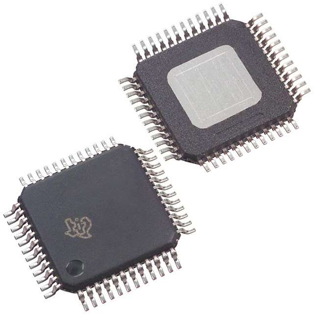
Package: 48-Pin HTQFP PowerPad™,
TJA = 28.8°C/W
2 Applications
•
•
•
•
Cellular Base Transceiver Station Transmit
Channel:
– CDMA: WCDMA, CDMA2000, IS-95
– TDMA: GSM, IS-136, EDGE/GPRS
– Supports Single-Carrier and Multicarrier
Applications
Test and Measurement: Arbitrary Waveform
Generation
Direct Digital Synthesis (DDS)
Cable Modem Headend
The DAC5675A operates from a single-supply
voltage of 3.3 V. Power dissipation is 660 mW at
fCLK = 400 MSPS, fOUT = 70 MHz. The DAC5675A
provides a nominal full-scale differential current
output of 20mA, supporting both single-ended and
differential applications. The output current can be
directly fed to the load with no additional external
output buffer required. The output is referred to the
analog supply voltage AVDD.
The DAC5675A comprises a low-voltage differential
signaling (LVDS) interface for high-speed digital data
input. LVDS features a low differential voltage swing
with a low constant power consumption across
frequency, allowing for high-speed data transmission
with low noise levels; that is, with low electromagnetic
interference (EMI). LVDS is typically implemented in
low-voltage digital CMOS processes, making it the
ideal technology for high-speed interfacing between
the DAC5675A and high-speed low-voltage CMOS
ASICs or FPGAs. The DAC5675A current-sink-array
architecture supports update rates of up to 400MSPS.
On-chip edge-triggered input latches provide for
minimum setup and hold times, thereby relaxing
interface timing.
Device Information(1)
PART NUMBER
DAC5675A
BODY SIZE (NOM)
PHP (48)
7.00 mm x 7.00 mm
(1) For all available packages, see the orderable addendum at
the end of the data sheet.
Simple Schematic
SLEEP
DAC5675A
Bandgap
Reference
1.2V
3 Description
The DAC5675A is a 14-bit resolution high-speed
digital-to-analog converter. The DAC5675A is
designed for high-speed digital data transmission in
wired and wireless communication systems, highfrequency direct-digital synthesis (DDS), and
waveform reconstruction in test and measurement
applications. The DAC5675A has excellent spuriousfree dynamic range (SFDR) at high intermediate
frequencies, which makes the DAC5675A well-suited
for multicarrier transmission in TDMA- and CDMAbased cellular base transceiver stations (BTSs).
PACKAGE
EXTIO
BIASJ
Current
Source
Array
Output
Current
Switches
Decoder
DAC
Latch
+
Drivers
Control Amp
14
D[13:0]A
LVDS
Input
Interface
D[13:0]B
Input
Latches
14
CLK
Clock Distribution
CLKC
AVDD (4x) AGND(4x)
DVDD(2x) DGND(2x)
Copywright © 2016, Texas Instruments Incorporated
1
An IMPORTANT NOTICE at the end of this data sheet addresses availability, warranty, changes, use in safety-critical applications,
intellectual property matters and other important disclaimers. PRODUCTION DATA.
�DAC5675A
SBAS334D – NOVEMBER 2004 – REVISED JULY 2016
www.ti.com
Table of Contents
1
2
3
4
5
6
7
Features ..................................................................
Applications ...........................................................
Description .............................................................
Revision History.....................................................
Description Continued ..........................................
Pin Configuration and Functions .........................
Specifications.........................................................
7.1
7.2
7.3
7.4
7.5
7.6
7.7
7.8
7.9
8
1
1
1
2
2
3
4
Absolute Maximum Ratings ..................................... 4
ESD Ratings.............................................................. 4
Recommended Operating Conditions....................... 5
Thermal Information .................................................. 5
DC Electrical Characteristics .................................... 6
AC Electrical Characteristics..................................... 7
Digital Specifications ................................................. 8
Operational Characteristics ...................................... 8
Typical Characteristics ............................................ 10
Detailed Description ............................................ 12
8.1 Overview ................................................................. 12
8.2 Functional Block Diagram ....................................... 12
8.3 Feature Description................................................. 12
8.4 Device Functional Modes........................................ 19
9
Application and Implementation ........................ 20
9.1 Application Information............................................ 20
9.2 Typical Application ................................................. 20
10 Power Supply Recommendations ..................... 21
11 Layout................................................................... 22
11.1 Layout Guidelines ................................................. 22
11.2 Layout Example .................................................... 22
12 Device and Documentation Support ................. 24
12.1
12.2
12.3
12.4
12.5
12.6
Receiving Notification of Documentation Updates
Community Resources..........................................
Trademarks ...........................................................
Electrostatic Discharge Caution ............................
Glossary ................................................................
Device Nomenclature............................................
24
24
24
24
24
24
13 Mechanical, Packaging, and Orderable
Information ........................................................... 25
4 Revision History
NOTE: Page numbers for previous revisions may differ from page numbers in the current version.
Changes from Revision C (March 2005) to Revision D
Page
•
Added ESD Ratings, Recommended Operating Conditions, Thermal Information, Detailed Description section,
Application and Implementation section, Power Supply Recommendations section, Layout section, Device and
Documentation Support section, Mechanical, Packaging, and Orderable Information section.............................................. 1
•
Changed AVDD to DVDD From: –3.6 to +3.6 To: –0.7 to +0.7 in the Absolute Maximum Ratings ......................................... 4
5 Description Continued
The DAC5675A has been specifically designed for a differential transformer-coupled output with a 50 Ω doublyterminated load. With the 20 mA full-scale output current, both a 4:1 impedance ratio (resulting in an output
power of 4 dBm) and 1:1 impedance ratio transformer (–2 dBm) are supported. The last configuration is preferred
for optimum performance at high output frequencies and update rates. The outputs are terminated to AVDD and
have voltage compliance ranges from AVDD –1 to AVDD + 0.3 V.
An accurate on-chip 1.2-V temperature-compensated bandgap reference and control amplifier allows the user to
adjust this output current from 20 mA down to 2 mA. This provides 20-dB gain range control capabilities.
Alternatively, an external reference voltage may be applied. The DAC5675A features a SLEEP mode, which
reduces the standby power to approximately 18 mW.
The DAC5675A is available in a 48-pin HTQFP thermally-enhanced PowerPad package. This package increases
thermal efficiency in a standard size IC package. The device is characterized for operation over the industrial
temperature range of –40°C to +85°C.
2
Submit Documentation Feedback
Copyright © 2004–2016, Texas Instruments Incorporated
Product Folder Links: DAC5675A
�DAC5675A
www.ti.com
SBAS334D – NOVEMBER 2004 – REVISED JULY 2016
6 Pin Configuration and Functions
AVDD
AGND
AGND
AVDD
IOUT2
IOUT1
AVDD
AGND
EXTIO
BIASJ
NC
SLEEP
48
47
46
45
44
43
42
41
40
39
38
37
PHP Package
48-Pin (HTQFP)
Top View
D13A
1
36
D0B
D13B
2
35
D0A
D12A
3
34
D1B
D12B
4
33
D1A
D11A
5
32
D2B
D11B
6
31
D2A
D10A
7
30
D3B
D10B
8
29
D3A
D9A
9
28
D4B
D9B
10
27
D4A
D8A
11
26
D5B
D8B
12
25
D5A
17
18
19
20
21
22
23
24
DVDD
DGND
AGND
AVDD
CLKC
CLK
D6A
D6B
15
DVDD
16
14
D7B
DGND
13
D7A
Thermal
Pad
Note: Thermal pad size: 4.5 mm x 4.5 mm (min), 5.5 mm x 5.5 mm (max)
Pin Functions
PIN
NAME
NO.
I/O
AGND
19, 41, 46, 47
I
DESCRIPTION
Analog negative supply voltage (ground); pin 47 internally connected to PowerPAD.
AVDD
20, 42, 45, 48
I
Analog positive supply voltage.
BIASJ
39
O
Full-scale output current bias.
CLK
22
I
External clock input.
CLKC
21
I
Complementary external clock input.
D(13:0)A
1, 3, 5, 7, 9, 11,
13, 23, 25, 27, 29,
31, 33, 35
I
LVDS positive input, data bits 0 through 13.
D13A is most significant data bit (MSB).
D0A is least significant data bit (MSB).
D(13:0)B
2, 4, 6, 8, 10, 12,
14, 24, 26, 28, 30,
32, 34, 36
I
LVDS negative input, data bits 0 through 13.
D13B is most significant data bit (MSB).
D0B is least significant data bit (MSB).
DGND
16, 18
I
Digital negative supply voltage (ground).
NC
38
-—
DVDD
15, 17
I
EXTIO
40
I/O
Internal reference output or external reference input. Requires a 0.1µF decoupling capacitor
to AGND when used as reference output.
IOUT1
43
O
DAC current output. Full-scale when all input bits are set to '0'. Connect reference side of
DAC load resistors to AVDD.
IOUT2
44
O
DAC complementary current output. Full-scale when all input bits are set to '1'. Connect
reference side of DAC load resistors to AVDD.
SLEEP
37
I
Asynchronous hardware power down input. Active high. Internal pulldown.
Not connected in chip. Can be high or low.
Digital positive supply voltage.
Submit Documentation Feedback
Copyright © 2004–2016, Texas Instruments Incorporated
Product Folder Links: DAC5675A
3
�DAC5675A
SBAS334D – NOVEMBER 2004 – REVISED JULY 2016
www.ti.com
7 Specifications
7.1
Absolute Maximum Ratings
over operating free-air temperature range (unless otherwise noted) (1)
Supply voltage range
MIN
MAX
UNIT
AVDD
(2)
–0.3
+3.6
V
DVDD
(3)
–0.3
+3.6
V
AVDD to DVDD
–0.7
+0.7
V
–0.3
+0.5
V
Voltage between AGND and DGND
CLK, CLKC
(2)
–0.3
AVDD + 0.3
V
Digital input D[13:0]A, D[13:0]B(3), SLEEP
–0.3
DVDD + 0.3
V
IOUT1, IOUT2 (2)
–1.0
AVDD + 0.3
V
–1.0
AVDD + 0.3
V
20
mA
EXTIO, BIAS
(2)
Peak input current (any input)
Peak total input current (all inputs)
-30
mA
Operating free-air temperature range, TA
–40
+85
°C
Storage temperature range
–65
+150
°C
(1)
(2)
(3)
Stresses above those listed under Absolute Maximum Ratings may cause permanent damage to the device. Exposure outside of
absolute maximum conditions for extended periods may degrade device reliability. These are stress ratings only, and functional
operation of the device at these or any other conditions beyond those indicated under recommended operating conditions is not implied.
Exposure to absolute-maximum-rated conditions for extended periods may affect device reliability.
Measured with respect to AGND.
Measured with respect to DGND.
7.2 ESD Ratings
VALUE
Human-body model (HBM), per ANSI/ESDA/JEDEC JS-001
V(ESD)
(1)
(2)
4
Electrostatic discharge
(1)
Charged-device model (CDM), per JEDEC specification JESD22C101 (2)
UNIT
±1000
±250
V
JEDEC document JEP155 states that 500-V HBM allows safe manufacturing with a standard ESD control process.
JEDEC document JEP157 states that 250-V CDM allows safe manufacturing with a standard ESD control process.
Submit Documentation Feedback
Copyright © 2004–2016, Texas Instruments Incorporated
Product Folder Links: DAC5675A
�DAC5675A
www.ti.com
SBAS334D – NOVEMBER 2004 – REVISED JULY 2016
7.3 Recommended Operating Conditions
over operating free-air temperature range (unless otherwise noted)
MIN
NOM
MAX
AVDD
3.15
3.3
3.6
DVDD
3.15
3.3
3.6
UNIT
Supplies
V
V
I(AVDD)
Analog supply current
115
mA
I(DVDD)
Digital supply current
85
mA
Analog Output
IO(FS)
Full-scale output current
Output compliance range
2
20
AVDD -1
AVDD + 0.3
mA
V
Clock Interface (CLK, CLKC)
CLKINPUT Frequency
|CLK – CLKC|
Clock duty cycle
VCM
Common-mode voltage range
400
MHz
0.4
0.8
VPP
40%
60%
1.6
2
2.4
V
7.4 Thermal Information
DAC5675A
THERMAL METRIC (1)
PHP (HTQFP)
UNIT
48 PINS
RθJA
Junction-to-ambient thermal resistance
31.3
°C/W
RθJC(top)
Junction-to-case (top) thermal resistance
13.0
°C/W
RθJB
Junction-to-board thermal resistance
10.9
°C/W
ψJT
Junction-to-top characterization parameter
0.3
°C/W
ψJB
Junction-to-board characterization parameter
10.9
°C/W
RθJC(bot)
Junction-to-case (bottom) thermal resistance
0.9
°C/W
(1)
For more information about traditional and new thermal metrics, see the SPRA953Semiconductor and IC Package Thermal Metrics
application report.
Submit Documentation Feedback
Copyright © 2004–2016, Texas Instruments Incorporated
Product Folder Links: DAC5675A
5
�DAC5675A
SBAS334D – NOVEMBER 2004 – REVISED JULY 2016
www.ti.com
7.5 DC Electrical Characteristics
Over operating free-air temperature range. Typical values at +25°C, AVDD = 3.3V, DVDD = 3.3V, IO(FS) = 20mA, unless
otherwise noted.
PARAMETER
TEST CONDITIONS
Resolution
MIN
TYP
MAX
14
DC Accuracy
UNIT
Bit
(1)
INL
Integral nonlinearity
DNL
Differential nonlinearity
TMIN to TMAX
Monotonicity
–4
±1.5
4
LSB
–2
±0.6
2
LSB
2
20
mA
AVDD – 1
AVDD +0.3
Monotonic 12b Level
Analog Output
IO(FS)
Full-scale output current
Output compliance range
AVDD = 3.15V to 3.45V, IO(FS) = 20mA
Offset error
0.01
Gain error
V
%FSR
Without internal reference
–10
5
10
%FSR
With internal reference
–10
2.5
10
%FSR
Output resistance
Output capacitance
300
kΩ
5
pF
Reference Output
V(EXTIO)
Reference voltage
1.17
Reference output current
(2)
1.23
1.29
100
V
nA
Reference Input
V(EXTIO)
Input reference voltage
0.6
Input resistance
1.2
1.25
V
1
MΩ
Small-signal bandwidth
1.4
MHz
Input capacitance
100
pF
12
ppm of
FSR/°C
±50
ppm/°C
Temperature Coefficients
Offset drift
Δ V(EXTIO)
Reference voltage drift
Power Supply
AVDD
Analog supply voltage
3.15
3.3
3.6
V
DVDD
Digital supply voltage
3.15
3.3
3.6
V
(3)
I(AVDD)
Analog supply current
I(DVDD)
Digital supply current (3)
PD
Power dissipation
Sleep mode
PD
Power dissipation
AVDD = 3.3V, DVDD = 3.3V
APSRR
Analog and digital powersupply rejection ratio
DPSRR
(1)
(2)
(3)
6
115
AVDD = 3.15V to 3.45V
mA
85
mA
18
mW
660
900
mW
–0.5
±0.1
0.5
%FSR/V
–0.5
±0.1
0.5
%FSR/V
Measured differential at IOUT1 and IOUT2; 25Ω to AVDD.
Use an external buffer amplifier with high impedance input to drive any external load.
Measured at fCLK = 400MSPS and fOUT = 70MHz.
Submit Documentation Feedback
Copyright © 2004–2016, Texas Instruments Incorporated
Product Folder Links: DAC5675A
�DAC5675A
www.ti.com
SBAS334D – NOVEMBER 2004 – REVISED JULY 2016
7.6 AC Electrical Characteristics
Over operating free-air temperature range. Typical values at +25°C, AVDD = 3.3V, DVDD = 3.3V, IO(FS) = 20mA, differential
transformer-coupled output, 50Ω doubly-terminated load, unless otherwise noted.
PARAMETER
TEST CONDITIONS
MIN
TYP
MAX
UNIT
400
MSPS
Analog Output
fCLK
Output update rate
ts(DAC)
Output setting time to 0.1%
tPD
Output propagation delay
tr(IOUT)
Output rise time, 10% to 90%
tf(IOUT)
Output fall time, 90% to 10%
Output noise (1)
Transition: code x2000 to x23FF
12
ns
1
ns
300
ps
300
ps
IOUTFS = 20mA
55
pA/√Hz
IOUTFS = 2mA
30
pA/√Hz
fCLK = 100MSPS, fOUT = 19.9MHz
73
dBc
fCLK = 160MSPS, fOUT = 41MHz
72
dBc
fCLK = 200MSPS, fOUT = 70MHz
68
dBc
fCLK = 400MSPS, fOUT = 20.1MHz
72
dBc
fCLK = 400MSPS, fOUT = 70MHz
71
dBc
fCLK = 400MSPS, fOUT = 140MHz
58
dBc
fCLK = 100MSPS, fOUT = 19.9MHz
73
dBc
fCLK = 160MSPS, fOUT = 41MHz
73
dBc
fCLK = 200MSPS, fOUT = 70MHz
70
dBc
fCLK = 400MSPS, fOUT = 20.1MHz
73
dBc
fCLK = 400MSPS, fOUT = 70MHz
74
dBc
fCLK = 400MSPS, fOUT = 140MHz
60
dBc
fCLK = 100MSPS, fOUT = 19.9MHz
88
dBc
fCLK = 160MSPS, fOUT = 41MHz
87
dBc
fCLK = 200MSPS, fOUT = 70MHz
82
dBc
fCLK = 400MSPS, fOUT = 20.1MHz
87
dBc
fCLK = 400MSPS, fOUT = 70MHz
82
dBc
fCLK = 400MSPS, fOUT = 140MHz
75
dBc
fCLK = 122.88MSPS, IF = 30.72MHz (2)
73
dB
(3)
AC Linearity
THD
SFDR
SFDR
ACPR
Total harmonic distortion
Spurious-free dynamic range
to Nyquist
Spurious-free dynamic range
within a window, 5MHz span
Adjacent channel power ratio
WCDMA with 3.84MHz BW,
5MHz channel spacing
Two-tone intermodulation to
Nyquist (each tone at -6dBfs)
IMD
(1)
(2)
(3)
(4)
Four-tone intermodulation,
15MHz span, missing center
tone (each tone at -16dBfs)
fCLK = 245.76MSPS, IF = 61.44MHz
71
dB
fCLK = 399.32MSPS, IF = 153.36MHz (4)
65
dB
fCLK = 400MSPS, fOUT1 = 70MHz,
fOUT2 = 71MHz
73
dBc
fCLK = 400MSPS, fOUT1 = 140MHz,
fOUT2 = 141MHz
62
dBc
fCLK = 156MSPS, fOUT = 15.6, 15.8, 16.2,
16.4MHz
82
dBc
fCLK = 400MSPS, fOUT = 68.1, 69.3, 71.2,
72MHz
74
dBc
Noise averaged up to 400MHz when operating at 400MSPS.
See Figure 9.
See Figure 10.
See Figure 12
Submit Documentation Feedback
Copyright © 2004–2016, Texas Instruments Incorporated
Product Folder Links: DAC5675A
7
�DAC5675A
SBAS334D – NOVEMBER 2004 – REVISED JULY 2016
www.ti.com
7.7 Digital Specifications
Over operating free-air temperature range. Typical values at +25°C, AVDD = 3.3V, DVDD = 3.3V, unless otherwise noted.
PARAMETER
TEST CONDITIONS
MIN
TYP
MAX
UNIT
LVDS Interface: nodes D[13:0]A, D[13:0]B
VITH+
Positive-going differential input voltage
threshold
VITH-
Negative-going differential input voltage
threshold
ZT
Internal termination impedance
CI
Input capacitance
See LVDS min/max
threshold voltages table
90
100
mV
-100
mV
110
132
2
Ω
pF
CMOS Interface (SLEEP):
VIH
High-level input voltage
VIL
Low-level input voltage
2
IIH
High-level input current
–100
IIL
Low-level input current
–10
3.3
V
0
Input capacitance
0.8
V
100
µA
10
µA
2
pF
Clock Interface (CLK, CLKC):
|CLKCLKC|
Clock differential input voltage
0.4
Clock duty cycle
VCM
0.8
40%
Common-mode voltage range
VPP
60%
2 ±20%
V
Input resistance
Node CLK, CLKC
670
Ω
Input capacitance
Node CLK, CLKC
2
pF
Input resistance
Differential
1.3
kΩ
Input capacitance
Differential
1
pF
Timing
tSU
Input setup time
1.5
tH
Input hold time
tDD
Digital delay time (DAC latency)
ns
0
ns
3
clk
7.8 Operational Characteristics (1)
Over operating free-air temperature range, AVDD = 3.3V, DVDD = 3.3V, IO(FS) = 20mA, unless otherwise noted.
APPLIED
VOLTAGES
RESULTING
COMMON-MODE
INPUT VOLTAGE
VA,B [mV]
VCOM [V]
LOGICAL BIT
BINARY
EQUIVALENT
VA [V]
VB [V]
1.25
1.15
100
1.2
1
1.15
1.25
–100
1.2
0
2.4
2.3
100
2.35
1
2.3
2.4
–100
2.35
0
(1)
8
RESULTING
DIFFERENTIAL
INPUT VOLTAGE
0.1
0
100
0.05
1
0
0.1
–100
0.05
0
1.5
0.9
600
1.2
1
0.9
1.5
–600
1.2
0
2.4
1.8
600
2.1
1
1.8
2.4
–600
2.1
0
0.6
0
600
0.3
1
0
0.6
–600
0.3
0
COMMENT
Operation with minimum differential voltage
(±100mV) applied to the complementary inputs
versus common-mode range
Operation with maximum differential voltage
(±600mV) applied to the complementary inputs
versus common-mode range
Specifications subject to change.
Submit Documentation Feedback
Copyright © 2004–2016, Texas Instruments Incorporated
Product Folder Links: DAC5675A
�DAC5675A
www.ti.com
SBAS334D – NOVEMBER 2004 – REVISED JULY 2016
D[13:0]A
Valid Data
D[13:0]B
tH
tSU
tDD
CLK
50%
50%
CLKC
tS(DAC)
tPD
0.1%
DAC Output
IOUT1/IOUT2
50%
90%
10%
0.1%
tr(IOUT)
Figure 1. Timing Diagram
DVDD
DAC5675A
VA
1.4V
VB
1V
VA, B
VA, B
0.4V
0V
−0.4V
VCOM =
VA + VB
VA
Logical Bit
Equivalent
2
VB
DGND
1
0
Copywright © 2016, Texas Instruments Incorporated
Figure 2. LVDS Timing Test Circuit and Input Test Levels
Submit Documentation Feedback
Copyright © 2004–2016, Texas Instruments Incorporated
Product Folder Links: DAC5675A
9
�DAC5675A
SBAS334D – NOVEMBER 2004 – REVISED JULY 2016
www.ti.com
7.9 Typical Characteristics
1.0
1.5
0.8
1.0
0.6
0.5
INL (LSB)
DNL (LSB)
0.4
0.2
0
- 0.2
0
- 0.5
- 0.4
- 0.6
- 1.0
- 0.8
- 1.0
- 1.5
0
2000
6000
8000 10000 12000 14000 16000
0
2000
4000
Figure 3. Differential Non-Linearity (DNL) vs Input Code
Figure 4. Integral Non-Linearity (INL) vs Input Code
- 30
- 40
Two−Tone IMD3 (dBc)
f1 = 69.5MHz, −6dBFS
f2 = 70.5MHz, −6dBFS
IMD3 = 77.41dBc
VCC = VAA = 3.3V
fCLK = 200MHz
- 20
- 50
- 60
- 70
- 80
- 90
- 100
67
65
69
71
73
90
88
86
84
82
80
78
76
74
72
70
68
66
64
62
60
75
f 2 - f1 = 1MHz (- 6dBFS each)
VCC = VAA = 3.3V
f CLK = 200MHz
5
15
25
35
Frequency (MHz)
0
- 20
- 40
- 50
40.06MHz
65
75
85
VCC = VAA = 3.3V
fCLK = 400MHz
86
- 3dBFS
82
78
74
- 6dBFS
70
0dBFS
66
62
60.25MHz
- 70
90
SFDR (dBFS)
- 30
- 60
55
Figure 6. Two-Tone IMD3 vs Frequency
VCC = VAA = 3.3V
f CLK = 400MHz
f OUT = 20.1MHz, 0dBFS
SFDR = 74.75dBc
20.1MHz
- 10
45
Center Frequency (MHz)
Figure 5. Two-Tone IMD (Power) vs Frequency
Power (dBFS)
8000 10000 12000 14000 16000
Input Code
0
58
- 80
54
50
- 90
0
10
6000
Input Code
- 10
Power (dBFS)
4000
20
40
60
80
100 120 140
160 180
200
10
20
30
40
50
60
70
80
90
100 110 120
Frequency (MHz)
Output Frequency (MHz)
Figure 7. Single-Tone Spectrum Power vs Frequency
Figure 8. Spurious-Free Dynamic Range vs Frequency
Submit Documentation Feedback
Copyright © 2004–2016, Texas Instruments Incorporated
Product Folder Links: DAC5675A
�DAC5675A
www.ti.com
SBAS334D – NOVEMBER 2004 – REVISED JULY 2016
Typical Characteristics (continued)
90
86
SFDR (dBFS)
78
74
- 6dBFS
70
0dBFS
66
62
VCC = VAA = 3.3V
fCLK = 122.88MHz
fCENTER = 30.72MHz
ACLR = 72.29dB
- 35
Power (dBm/30kHz)
- 3dBFS
82
- 25
VCC = VAA = 3.3V
fCLK = 200MHz
- 45
- 55
- 65
- 75
- 85
58
- 95
54
- 105
50
- 115
10
20
30
40
50
60
70
80
90
100 110 120
23
18
28
Output Frequency (MHz)
Figure 9. Spurious-Free Dynamic Range vs Frequency
- 30
V CC = V AA = 3.3V
38
43
Figure 10. W-CDMA TM1 Single Carrier Power vs Frequency
80
f CLK = 368.64MHz
- 40 fCENTER =
VCC = VAA = 3.3V
fCLK = 399.36MHz
Single Channel
78
ACLR = 65dBc
92.16MHz
76
- 50
74
ACLR (dBc)
Power (dBm/30kHz)
33
Frequency
- 60
- 70
- 80
72
70
68
66
- 90
64
- 100
- 110
82.2
62
60
87.2
92.2
97.2
10.2
10
30
50
70
90
110
130
150
Frequency
Output Frequency (MHz)
Figure 11. W-CDMA TM1 Dual Carrier Power vs Frequency
Figure 12. W-CDMA TM1 Single Carrier ACLR vs Output
Frequency
Submit Documentation Feedback
Copyright © 2004–2016, Texas Instruments Incorporated
Product Folder Links: DAC5675A
11
�DAC5675A
SBAS334D – NOVEMBER 2004 – REVISED JULY 2016
www.ti.com
8 Detailed Description
8.1 Overview
The DAC5675A is a 14-bit resolution high-speed digital-to-analog converter. The DAC5675A is designed or highspeed digital data transmission in wired and wireless communication systems, high frequency direct-digital
synthesis (DDS), and waveform reconstruction in test and measurement applications. The DAC5675A has
excellent spurious free dynamic range (SFDR) at high intermediate frequencies, which makes the DAC5675A
well-suited for multicarrier transmission in TDMA- and CDMA based cellular base transceiver stations (BTSs).
8.2 Functional Block Diagram
SLEEP
DAC5675A
Bandgap
Reference
1.2V
EXTIO
BIASJ
Current
Source
Array
Output
Current
Switches
Decoder
DAC
Latch
+
Drivers
Control Amp
14
D[13:0]A
LVDS
Input
Interface
D[13:0]B
Input
Latches
14
CLK
Clock Distribution
CLKC
AVDD (4x) AGND(4x)
DVDD(2x) DGND(2x)
Copywright © 2016, Texas Instruments Incorporated
8.3 Feature Description
8.3.1 Digital Inputs
The DAC5675A uses a low voltage differential signaling (LVDS) bus input interface. The LVDS features a low
differential voltage swing with low constant power consumption (≉4mA per complementary data input) across
frequency. The differential characteristic of LVDS allows for high-speed data transmission with low
electromagnetic interference (EMI) levels. The LVDS input minimum and maximum input threshold table lists the
LVDS input levels. Figure 13 shows the equivalent complementary digital input interface for the DAC5675A, valid
for pins D[13:0]A and D[13:0]B. Note that the LVDS interface features internal 110Ω resistors for proper
termination. Figure 2 shows the LVDS input timing measurement circuit and waveforms. A common-mode level
of 1.2V and a differential input swing of 0.8VPP is applied to the inputs.
Figure 14 shows a schematic of the equivalent CMOS/TTL-compatible digital inputs of the DAC5675A, valid for
the SLEEP pin.
12
Submit Documentation Feedback
Copyright © 2004–2016, Texas Instruments Incorporated
Product Folder Links: DAC5675A
�DAC5675A
www.ti.com
SBAS334D – NOVEMBER 2004 – REVISED JULY 2016
Feature Description (continued)
DVDD
DAC5675A
DAC5675A
D[13..0]A
110W
Termination
Resistor
Internal
Digital IN
D[13..0]B
D[13..0]A
D[13..0]B
Internal
Digital In
DGND
Copywright © 2016, Texas Instruments Incorporated
Figure 13. LVDS Digital Equivalent Input
DVDD
DAC5675A
Digital Input
Internal
Digital In
DGND
Copywright © 2016, Texas Instruments Incorporated
Figure 14. CMOS/TTL Digital Equivalent Input
Submit Documentation Feedback
Copyright © 2004–2016, Texas Instruments Incorporated
Product Folder Links: DAC5675A
13
�DAC5675A
SBAS334D – NOVEMBER 2004 – REVISED JULY 2016
www.ti.com
Feature Description (continued)
8.3.2 Clock Input
The DAC5675A features differential, LVPECL compatible clock inputs (CLK, CLKC). Figure 15 shows the
equivalent schematic of the clock input buffer. The internal biasing resistors set the input common-mode voltage
to approximately 2V, while the input resistance is typically 670Ω. A variety of clock sources can be ac-coupled to
the device, including a sine wave source (see Figure 16).
AVDD
DAC5675A
R1
1kW
R1
1kW
Internal
Clock
CLK
CLKC
R2
2kW
R2
2kW
AGND
Copywright © 2016, Texas Instruments Incorporated
Figure 15. Clock Equivalent Input
Optional, may be
bypassed for sine
wave input.
Swing Limitation
CAC
0.1mF
1:4
CLK
RT
200W
DAC5675A
CLKC
Termination
Resistor
Copywright © 2016, Texas Instruments Incorporated
Figure 16. Driving the DAC5675A with a Single-Ended Clock Source Using a Transformer
To obtain best ac performance the DAC5675A clock input should be driven with a differential LVPECL or sine
wave source as shown in Figure 17 and Figure 18. Here, the potential of VTT should be set to the termination
voltage required by the driver along with the proper termination resistors (RT). The DAC5675A clock input can
also be driven single-ended; this is shown in Figure 19.
14
Submit Documentation Feedback
Copyright © 2004–2016, Texas Instruments Incorporated
Product Folder Links: DAC5675A
�DAC5675A
www.ti.com
SBAS334D – NOVEMBER 2004 – REVISED JULY 2016
Feature Description (continued)
Single−Ended
ECL
or
(LV)PECL
Source
CAC
0.01mF
ECL/PECL
Gate
CLK
CAC
DAC5675A
0.01mF
CLKC
RT
50W
RT
50W
VTT
Copywright © 2016, Texas Instruments Incorporated
Figure 17. Driving the DAC5675A with a Single-Ended ECL/PECL Clock Source
CAC
0.01mF
Differential +
ECL
or
(LV)PECL
Source
−
CLK
CAC
DAC5675A
0.01mF
CLKC
RT
50W
RT
50W
VTT
Copywright © 2016, Texas Instruments Incorporated
Figure 18. Driving the DAC5675A with a Differential ECL/PECL Clock Source
TTL/CMOS
Source
CLK
R OPT
22W
DAC5675A
CLKC
0.01mF
Node CLKC
Internally biased to
AVDD/2
Copywright © 2016, Texas Instruments Incorporated
Figure 19. Driving the DAC5675A with a Single-Ended TTL/CMOS Clock Source
Submit Documentation Feedback
Copyright © 2004–2016, Texas Instruments Incorporated
Product Folder Links: DAC5675A
15
�DAC5675A
SBAS334D – NOVEMBER 2004 – REVISED JULY 2016
www.ti.com
Feature Description (continued)
8.3.3 Supply Inputs
The DAC5675A comprises separate analog and digital supplies, that is, AVDD and DVDD, respectively. These
supply inputs can be set independently from 3.6V down to 3.15V.
8.3.4 DAC Transfer Function
The DAC5675A has a current sink output. The current flow through IOUT1 and IOUT2 is controlled by D[13:0]A
and D[13:0]B. For ease of use, we denote D[13:0] as the logical bit equivalent of D[13:0]A and its complement
D[13:0]B. The DAC5675A supports straight binary coding with D13 being the MSB and D0 the LSB. Full-scale
current flows through IOUT2 when all D[13:0] inputs are set high and through IOUT1 when all D[13:0] inputs are
set low. The relationship between IOUT1 and IOUT2 can be expressed asEquation 1:
IOUT1 = IO(FS) - IOUT2
(1)
IO(FS) is the full-scale output current sink (2mA to 20mA). Since the output stage is a current sink, the current can
only flow from AVDD through the load resistors RL into the IOUT1 and IOUT2 pins.
The output current flow in each pin driving a resistive load can be expressed as shown in Figure 20, as well as in
Equation 2 and Equation 3.
DAC5675A
D[13:0] = 0
IOUT1
IOUT2
-
VOUT2
0mA
RL
VOUT1
-
+
RL
3.3V
AVDD
+
D[13:0] = 1
20mA
Copywright © 2016, Texas Instruments Incorporated
Figure 20. Relationship Between D[13:0], IOUT1 and IOUT2
IOUT1 =
IOUT2 =
IO(FS) x (16383 - CODE)
16384
IO(FS) x CODE
(2)
16384
(3)
where CODE is the decimal representation of the DAC input word. This would translate into single-ended
voltages at IOUT1 and IOUT2, as shown in Equation 4 and Equation 5:
VOUT1 = AVDD - IOUT1 x RL
(4)
VOUT2 = AVDD - IOUT2 x RL
(5)
Assuming that D[13:0] = 1 and the RL is 50Ω, the differential voltage between pins IOUT1 and IOUT2 can be
expressed as shown in Equation 6 through Equation 8:
VOUT1 = 3.3 V - 0 mA x 50 = 3.3 V
VOUT2 = AVDD - 20 mA x 50 = 2.3 V
VDIFF = VOUT1 - VOUT2 = 1 V
(6)
(7)
(8)
If D[13:0] = 0, then IOUT2 = 0mA and IOUT1 = 20mA and the differential voltage VDIFF = –1V.
The output currents and voltages in IOUT1 and IOUT2 are complementary. The voltage, when measured
differentially, will be doubled compared to measuring each output individually. Care must be taken not to exceed
the compliance voltages at the IOUT1 and IOUT2 pins in order to keep signal distortion low.
8.3.5 Reference Operation
The DAC5675A has a bandgap reference and control amplifier for biasing the full-scale output current. The fullscale output current is set by applying an external resistor RBIAS. The bias current IBIAS through resistor RBIAS is
defined by the on-chip bandgap reference voltage and control amplifier. The full-scale output current equals 16
times this bias current. The full-scale output current IO(FS) is thus expressed as Equation 9:
16
Submit Documentation Feedback
Copyright © 2004–2016, Texas Instruments Incorporated
Product Folder Links: DAC5675A
�DAC5675A
www.ti.com
SBAS334D – NOVEMBER 2004 – REVISED JULY 2016
Feature Description (continued)
IO(FS) = 16 x IBIAS =
16 x VEXTIO
RBIAS
(9)
where VEXTIO is the voltage at terminal EXTIO. The bandgap reference voltage delivers a stable voltage of 1.2 V.
This reference can be overridden by applying an external voltage to terminal EXTIO. The bandgap reference can
additionally be used for external reference operation. In such a case, an external buffer amplifier with high
impedance input should be selected in order to limit the bandgap load current to less than 100 nA. The capacitor
CEXT may be omitted. Terminal EXTIO serves as either an input or output node. The full-scale output current is
adjustable from 20mA down to 2mA by varying resistor RBIAS.
8.3.6 Analog Current Outputs
Figure 21 shows a simplified schematic of the current sink array output with corresponding switches. Differential
NPN switches direct the current of each individual NPN current sink to either the positive output node IOUT1 or
its complementary negative output node IOUT2. D[13:0] controls the S(N)C current switches and D[13:0] controls
the S(N) current switches, as explained in the previous DAC Transfer Function section (see Figure 20). The
output impedance is determined by the stack of the current sinks and differential switches, and is > 300kΩ in
parallel with an output capacitance of 5pF.
The external output resistors are referred to the positive supply AVDD.
3.3V
AVDD
RLOAD
RLOAD
IOUT1
IOUT2
DAC5675A
S(1)
S(1)C
S(2)
S(2)C S(N)
S(N)C
Current Sink Array
AGND
Copywright © 2016, Texas Instruments Incorporated
Figure 21. Equivalent Analog Current Output
The DAC5675A can easily be configured to drive a doubly-terminated 50Ω cable using a properly selected
transformer. Figure 22 and Figure 23 show the 1:1 and 4:1 impedance ratio configuration, respectively. These
configurations provide maximum rejection of common-mode noise sources and even-order distortion
components, thereby doubling the power of the DAC to the output. The center tap on the primary side of the
transformer is terminated to AVDD, enabling a dc current flow for both IOUT1 and IOUT2. Note that the ac
performance of the DAC5675A is optimum and specified using a 1:1 differential transformer-coupled output.
Submit Documentation Feedback
Copyright © 2004–2016, Texas Instruments Incorporated
Product Folder Links: DAC5675A
17
�DAC5675A
SBAS334D – NOVEMBER 2004 – REVISED JULY 2016
www.ti.com
Feature Description (continued)
3.3V
AVDD
DAC5675A
50W
1:1
IOUT1
RLOAD
50W
100W
IOUT2
50W
3.3V
AVDD
Copywright © 2016, Texas Instruments Incorporated
Figure 22. Driving a Doubly-Terminated 50Ω Cable Using a 1:1 Impedance Ratio Transformer
3.3V
AVDD
DAC5675A
100W
4:1
IOUT1
RLOAD
50W
IOUT2
15W
100W
3.3V
AVDD
Copywright © 2016, Texas Instruments Incorporated
Figure 23. Driving a Doubly-Terminated 50Ω Cable Using a 4:1 Impedance Ratio Transformer
Figure 24(a) shows the typical differential output configuration with two external matched resistor loads. The
nominal resistor load of 25 Ω gives a differential output swing of 1VPP (0.5–VPP single-ended) when applying a 20
mA full-scale output current. The output impedance of the DAC5675A slightly depends on the output voltage at
nodes IOUT1 and IOUT2. Consequently, for optimum dc-integral nonlinearity, the configuration of Figure 24(b)
should be chosen. In this current/voltage (I-V) configuration, terminal IOUT1 is kept at AVDD by the inverting
operational amplifier. The complementary output should be connected to AVDD to provide a dc-current path for
the current sources switched to IOUT1. The amplifier maximum output swing and the full-scale output current of
the DAC determine the value of the feedback resistor (RFB). The capacitor (CFB) filters the steep edges of the
DAC5675A current output, thereby reducing the operational amplifier slew-rate requirements. In this
configuration, the op amp should operate at a supply voltage higher than the resistor output reference voltage
AVDD as a result of its positive and negative output swing around AVDD. Node IOUT1 should be selected if a
single-ended unipolar output is desired.
18
Submit Documentation Feedback
Copyright © 2004–2016, Texas Instruments Incorporated
Product Folder Links: DAC5675A
�DAC5675A
www.ti.com
SBAS334D – NOVEMBER 2004 – REVISED JULY 2016
Feature Description (continued)
(a)
(b)
3.3V
AVDD
DAC5675A
CFB
200W (RFB)
DAC5675A
25W
IOUT1
VOUT1
IOUT2
VOUT2
IOUT1
VOUT
IOUT2
25W
3.3V
AVDD
Optional, for single−
ended output
referred to AVDD
3.3V
AVDD
Copywright © 2016, Texas Instruments Incorporated
Figure 24. Output Configurations
8.4 Device Functional Modes
8.4.1 Sleep Mode
The DAC5675A features a power-down mode that turns off the output current and reduces the supply current to
approximately 6mA. The power-down mode is activated by applying a logic level 1 to the SLEEP pin pulled down
internally.
Submit Documentation Feedback
Copyright © 2004–2016, Texas Instruments Incorporated
Product Folder Links: DAC5675A
19
�DAC5675A
SBAS334D – NOVEMBER 2004 – REVISED JULY 2016
www.ti.com
9 Application and Implementation
NOTE
Information in the following applications sections is not part of the TI component
specification, and TI does not warrant its accuracy or completeness. TI’s customers are
responsible for determining suitability of components for their purposes. Customers should
validate and test their design implementation to confirm system functionality.
9.1 Application Information
Figure 25 shows a simplified block diagram of the current steering DAC5675A. The DAC5675A consists of a
segmented array of NPN-transistor current sinks, capable of delivering a full-scale output current up to 20 mA.
Differential current switches direct the current of each current sink to either one of the complementary output
nodes IOUT1 or IOUT2. The complementary current output enables differential operation, canceling out
common-mode noise sources (digital feed-through, on-chip and PCB noise), dc offsets, and even-order distortion
components, and doubling signal output power.
The full-scale output current is set using an external resistor (RBIAS) in combination with an on-chip bandgap
voltage reference source (1.2 V) and control amplifier. The current (IBIAS) through resistor RBIAS is mirrored
internally to provide a full-scale output current equal to 16 times IBIAS. The full-scale current is adjustable from 20
mA down to 2 mA by using the appropriate bias resistor value.
9.2 Typical Application
A typical application for the DAC5675a is as dual or single carrier transmitter. The DAC is provided with some
input digital baseband signal and it outputs an analog carrier.
SLEEP
3.3V
(AVDD)
DAC5675A
Bandgap
Reference
1.2V
50W
IOUT
Output
1:1
EXTIO
Current
Source
Array
BIASJ
CEXT
0.1mF
Output
Current
Switches
Control Amp
RBIAS
1kW
IOUT
50W
RLOAD
50W
3.3V
(AVDD)
14
D[13:0]A
LVDS
Input
Interface
D[13:0]B
Input
Latches
DAC
Latch
+
Drivers
Decoder
14
3.3V
(AVDD)
CLK
1:4
Clock
Input
100W
RT
200W
Clock Distribution
CLKC
AVDD(4x)
AGND(4x)
DVDD(2x)
DGND(2x)
Copywright © 2016, Texas Instruments Incorporated
Figure 25. Application Schematic
20
Submit Documentation Feedback
Copyright © 2004–2016, Texas Instruments Incorporated
Product Folder Links: DAC5675A
�DAC5675A
www.ti.com
SBAS334D – NOVEMBER 2004 – REVISED JULY 2016
Typical Application (continued)
9.2.1 Design Requirements
The requirements for this design were to generate a 2-carrier WCDMA signal at an intermediate frequency of
92.16 MHz. The ACPR needs to be better than 65 dBc. For this design example use the parameters shown in
Table 1.
Table 1. Design Parameters
PARAMETER
VALUE
Clock rate
368.64 MHz
Input data
2C WCDMA with IF frequency at 92.16MHz
VCC / VAA
3.3 V
9.2.2 Detailed Design Procedure
The 2-carrier signal with an intermediate frequency of 92.16 MHz must be created in the digital processor at a
sample rate of 368.64 Msps for DAC. These 14 bit samples are placed on the 14b LVDS input port of the DAC.
A differential DAC clock must be generated from a clock source at 368.64 MHz. This must be provided to the
CLKIN pins of the DAC.
The IOUOTA and IOUTB differential connections must be connected to a transformer to provide a single ended
output. A typical 1:1 impedance transformer is used on the device EVM. The DAC5675AEVM (SLAU080)
provides a good reference for this design example.
9.2.3 Application Curves
This spectrum analyzer plot shows the ACPR for the transformer output 2-carrier signal with intermediate
frequency of 92.16 MHz. The results meet the system requirements for a minimum of 65 dBc ACPR.
- 30
V CC = V AA = 3.3V
f CLK = 368.64MHz
- 40 fCENTER =
ACLR = 65dBc
Power (dBm/30kHz)
92.16MHz
- 50
- 60
- 70
- 80
- 90
- 100
- 110
82.2
87.2
92.2
97.2
10.2
Frequency
Figure 26. W-CDMA TM1 Dual Carrier Power vs Frequency
10 Power Supply Recommendations
It is recommended that the device be powered with the nominal supply voltages as indicated in the
Recommended Operating Conditions.
In most instances the best performance is achieved with LDO supplies. However the supplies may be driven with
direct outputs from a DC-DC switcher as long as the noise performance of the switcher is acceptable.
Submit Documentation Feedback
Copyright © 2004–2016, Texas Instruments Incorporated
Product Folder Links: DAC5675A
21
�DAC5675A
SBAS334D – NOVEMBER 2004 – REVISED JULY 2016
www.ti.com
11 Layout
11.1 Layout Guidelines
The DAC5675 EVM layout should be used as a reference for the layout to obtain the best performance. A
sample layout is shown in Figure 27. Some important layout recommendations are:
• Use a single ground plane. Keep the digital and analog signals on distinct separate sections of the board.
This may be virtually divided down the middle of the device package when doing placement and layout.
• Keep the analog outputs as far away from the switching clocks and digital signals as possible. This will keep
coupling from the digital circuits to the analog outputs to a minimum.
• Decoupling caps should be kept close to the power pins of the device.
11.2 Layout Example
Figure 27. Top Layer of DAC5675A EVM Layout
22
Submit Documentation Feedback
Copyright © 2004–2016, Texas Instruments Incorporated
Product Folder Links: DAC5675A
�DAC5675A
www.ti.com
SBAS334D – NOVEMBER 2004 – REVISED JULY 2016
Layout Example (continued)
Figure 28. Bottom Layer of DAC5675A EVM Layout
Submit Documentation Feedback
Copyright © 2004–2016, Texas Instruments Incorporated
Product Folder Links: DAC5675A
23
�DAC5675A
SBAS334D – NOVEMBER 2004 – REVISED JULY 2016
www.ti.com
12 Device and Documentation Support
12.1 Receiving Notification of Documentation Updates
To receive notification of documentation updates — go to the product folder for your device on ti.com. In the
upper right-hand corner, click the Alert me button to register and receive a weekly digest of product information
that has changed (if any). For change details, check the revision history of any revised document.
12.2 Community Resources
The following links connect to TI community resources. Linked contents are provided "AS IS" by the respective
contributors. They do not constitute TI specifications and do not necessarily reflect TI's views; see TI's Terms of
Use.
TI E2E™ Online Community TI's Engineer-to-Engineer (E2E) Community. Created to foster collaboration
among engineers. At e2e.ti.com, you can ask questions, share knowledge, explore ideas and help
solve problems with fellow engineers.
Design Support TI's Design Support Quickly find helpful E2E forums along with design support tools and
contact information for technical support.
12.3 Trademarks
PowerPad, E2E are trademarks of Texas Instruments.
All other trademarks are the property of their respective owners.
12.4 Electrostatic Discharge Caution
These devices have limited built-in ESD protection. The leads should be shorted together or the device placed in conductive foam
during storage or handling to prevent electrostatic damage to the MOS gates.
12.5 Glossary
SLYZ022 — TI Glossary.
This glossary lists and explains terms, acronyms, and definitions.
12.6 Device Nomenclature
12.6.1 Definitions of Specifications and Terminology
Gain error is defined as the percentage error in the ratio between the measured full-scale output current and the
value of 16 x V(EXTIO)/RBIAS. A V(EXTIO) of 1.25V is used to measure the gain error with an external reference
voltage applied. With an internal reference, this error includes the deviation of V(EXTIO) (internal bandgap
reference voltage) from the typical value of 1.25V.
Offset error is defined as the percentage error in the ratio of the differential output current (IOUT1–IOUT2) and
the half of the full-scale output current for input code 8192.
THD is the ratio of the rms sum of the first six harmonic components to the rms value of the fundamental output
signal.
SNR is the ratio of the rms value of the fundamental output signal to the rms sum of all other spectral
components below the Nyquist frequency, including noise, but excluding the first six harmonics and dc.
SINAD is the ratio of the rms value of the fundamental output signal to the rms sum of all other spectral
components below the Nyquist frequency, including noise and harmonics, but excluding dc.
ACPR or adjacent channel power ratio is defined for a 3.84Mcps 3GPP W-CDMA input signal measured in a
3.84MHz bandwidth at a 5MHz offset from the carrier with a 12dB peak-to-average ratio.
APSSR or analog power supply ratio is the percentage variation of full-scale output current versus a 5% variation
of the analog power supply AVDD from the nominal. This is a dc measurement.
DPSSR or digital power supply ratio is the percentage variation of full-scale output current versus a 5% variation
of the digital power supply DVDD from the nominal. This is a dc measurement.
24
Submit Documentation Feedback
Copyright © 2004–2016, Texas Instruments Incorporated
Product Folder Links: DAC5675A
�DAC5675A
www.ti.com
SBAS334D – NOVEMBER 2004 – REVISED JULY 2016
13 Mechanical, Packaging, and Orderable Information
The following pages include mechanical, packaging, and orderable information. This information is the most
current data available for the designated devices. This data is subject to change without notice and revision of
this document. For browser-based versions of this data sheet, refer to the left-hand navigation.
Submit Documentation Feedback
Copyright © 2004–2016, Texas Instruments Incorporated
Product Folder Links: DAC5675A
25
�PACKAGE OPTION ADDENDUM
www.ti.com
10-Dec-2020
PACKAGING INFORMATION
Orderable Device
Status
(1)
Package Type Package Pins Package
Drawing
Qty
Eco Plan
(2)
Lead finish/
Ball material
MSL Peak Temp
Op Temp (°C)
Device Marking
(3)
(4/5)
(6)
DAC5675AIPHP
ACTIVE
HTQFP
PHP
48
250
RoHS & Green
NIPDAU
Level-3-260C-168 HR
-40 to 85
DAC5675AI
(1)
The marketing status values are defined as follows:
ACTIVE: Product device recommended for new designs.
LIFEBUY: TI has announced that the device will be discontinued, and a lifetime-buy period is in effect.
NRND: Not recommended for new designs. Device is in production to support existing customers, but TI does not recommend using this part in a new design.
PREVIEW: Device has been announced but is not in production. Samples may or may not be available.
OBSOLETE: TI has discontinued the production of the device.
(2)
RoHS: TI defines "RoHS" to mean semiconductor products that are compliant with the current EU RoHS requirements for all 10 RoHS substances, including the requirement that RoHS substance
do not exceed 0.1% by weight in homogeneous materials. Where designed to be soldered at high temperatures, "RoHS" products are suitable for use in specified lead-free processes. TI may
reference these types of products as "Pb-Free".
RoHS Exempt: TI defines "RoHS Exempt" to mean products that contain lead but are compliant with EU RoHS pursuant to a specific EU RoHS exemption.
Green: TI defines "Green" to mean the content of Chlorine (Cl) and Bromine (Br) based flame retardants meet JS709B low halogen requirements of