DAC5687
www.ti.com
SLWS164E – FEBRUARY 2005 – REVISED SEPTEMBER 2006
16-BIT, 500 MSPS 2×–8× INTERPOLATING DUAL-CHANNEL
DIGITAL-TO-ANALOG CONVERTER (DAC)
FEATURES
1
•
•
•
•
2345
•
•
•
•
•
•
•
•
•
500 MSPS
Selectable 2×–8× Interpolation
On-Chip PLL/VCO Clock Multiplier
Full IQ Compensation Including Offset, Gain,
and Phase
Flexible Input Options:
– FIFO With Latch on External or Internal
Clock
– Even/Odd Multiplexed Input
– Single Port Demultiplexed Input
Complex Mixer With 32-Bit NCO
Fixed Frequency Mixer With fS/4 and fS/2
1.8-V or 3.3-V I/O Voltage
On-Chip 1.2-V Reference
Differential Scalable Output: 2 mA to 20 mA
Pin Compatible to DAC5686
High Performance
– 81-dBc ACLR WCDMA TM1 at 30.72 MHz
– 72-dBc ACLR WCDMA TM1 at 153.6 MHz
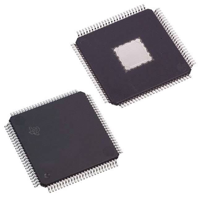
Package: 100-Pin HTQFP
APPLICATIONS
•
•
Cellular Base Transceiver Station Transmit
Channel
– CDMA: W-CDMA, CDMA2000, TD-SCDMA
– TDMA: GSM, IS-136, EDGE/UWC-136
– OFDM: 802.16
Cable Modem Termination System
DESCRIPTION
The DAC5687 is a dual-channel 16-bit high-speed
digital-to-analog converter (DAC) with integrated 2×,
4×, and 8× interpolation filters, a complex numerically
controlled oscillator (NCO), onboard clock multiplier,
IQ compensation, and on-chip voltage reference. The
DAC5687 is pin-compatible to the DAC5686,
requiring only changes in register settings for most
applications, and offers additional features and
superior linearity, noise, crosstalk, and PLL phase
noise performance.
The DAC5687 has six signal processing blocks: two
interpolate-by-two digital filters, a fine frequency
mixer with 32-bit NCO, a quadrature modulation
compensation block, another interpolate-by-two digital
filter, and a coarse frequency mixer with fS/2 or fS/4.
The different modes of operation enable or bypass
the signal processing blocks.
The coarse and fine mixers can be combined to span
a wider range of frequencies with fine resolution. The
DAC5687 allows both complex or real output.
Combining the frequency upconversion and complex
output produces a Hilbert transform pair that is output
from the two DACs. An external RF quadrature
modulator then performs the final single-sideband
upconversion.
The IQ compensation feature allows optimization of
phase, gain, and offset to maximize sideband
rejection and minimize LO feedthrough for an analog
quadrature modulator.
The DAC5687 includes several input options:
single-port interleaved data, even and odd
multiplexing at half-rate, and an input FIFO with either
external or internal clock to ease the input timing
ambiguity when the DAC5687 is clocked at the DAC
output sample rate.
ORDERING INFORMATION
TA
Package Device
–40°C to 85°C
100 HTQFP (1) (PZP) PowerPAD™
package, plastic quad flatpack
DAC5687IPZP
(1)
Thermal pad size: 6 mm × 6 mm.
1
2
3
4
5
Please be aware that an important notice concerning availability, standard warranty, and use in critical applications of
Texas Instruments semiconductor products and disclaimers thereto appears at the end of this data sheet.
PowerPAD is a trademark of Texas Instruments.
Excel is a trademark of Microsoft Corporation.
Matlab is a trademark of The MathWorks, Inc.
All other trademarks are the property of their respective owners.
PRODUCTION DATA information is current as of publication date.
Products conform to specifications per the terms of the Texas
Instruments standard warranty. Production processing does not
necessarily include testing of all parameters.
Copyright © 2005–2006, Texas Instruments Incorporated
�DAC5687
www.ti.com
SLWS164E – FEBRUARY 2005 – REVISED SEPTEMBER 2006
These devices have limited built-in ESD protection. The leads should be shorted together or the device placed in conductive foam
during storage or handling to prevent electrostatic damage to the MOS gates.
FUNCTIONAL BLOCK DIAGRAM
CLKVDD
CLKGND
PLLGND
LPF
PLLVDD
PHSTR
SLEEP
DVDD
CLK1
CLK1C
1.2-V
Reference
Internal Clock Generation
and
2y–8y PLL Clock Multiplier
CLK2
DGND
EXTIO
EXTLO
2y–8y fDATA
BIASJ
CLK2C
A
Offset
A Gain
PLLLOCK
FIR1
FIR2
FIR4
FIR3
y2
y2
Fine Mixer
y2
x
sin(x)
16-Bit
DAC
x
sin(x)
16-Bit
DAC
IOUTA1
IOUTA2
Course Mixer:
fs/2 or fs/4
y2
Input FIFO/
Reorder/
Mux/Demux
y2
Quadrature Mod
Correction (QMC)
DA[15:0]
DB[15:0]
y2
IOUTB1
IOUTB2
TXENABLE
RESETB
cos
QFLAG
SIF
sin
B
Offset
IOGND
B Gain
IOVDD
NCO
100-Pin HTQFP
SDIO
SDO SDENB SCLK
AVDD
AGND
B0019-02
2
Submit Documentation Feedback
Copyright © 2005–2006, Texas Instruments Incorporated
Product Folder Link(s): DAC5687
�DAC5687
www.ti.com
SLWS164E – FEBRUARY 2005 – REVISED SEPTEMBER 2006
PINOUT
DGND
IOVDD
IOGND
DB7
DB6
DB5
81
80
79
78
77
76
DB8
DVDD
83
82
DB10
DB9
DB11
85
DB12
87
86
84
DVDD
DGND
89
88
DB14
DB13
91
DB15 (MSB or LSB)
92
90
PHSTR
DGND
94
93
SLEEP
RESETB
95
TESTMODE
96
QFLAG
98
97
AVDD
DVDD
AVDD
DGND
1
99
AGND
100
PZP PACKAGE
(TOP VIEW)
75
DB4
2
74
DB3
3
73
DB2
AGND
4
72
DB1
IOUTB1
5
71
DB0 (LSB or MSB)
IOUTB2
6
70
PLLLOCK
AGND
7
69
DGND
AVDD
8
68
DVDD
AGND
9
67
PLLVDD
AVDD
10
66
LPF
EXTIO
11
65
PLLGND
AGND
12
64
CLKGND
BIASJ
13
63
CLK2C
AVDD
14
62
CLK2
EXTLO
15
61
CLKVDD
AVDD
16
60
CLK1C
AGND
17
59
CLK1
AVDD
18
58
CLKGND
DAC5687
47
48
49
50
IOGND
DA7
DA6
DA5
45
46
DGND
IOVDD
43
DA9
44
DA10
DA8
41
42
DA11
DVDD
39
40
DA12
37
38
DVDD
DGND
35
36
DA14
DA13
DA4
34
51
DA15 (MSB or LSB)
25
32
AGND
33
DA3
DVDD
DA2
52
TXENABLE
53
24
30
23
AVDD
31
AVDD
SDO
DA1
SDIO
DA0 (LSB or MSB)
54
28
55
22
29
21
AGND
SCLK
IOUTA1
SDENB
DVDD
26
DGND
56
27
57
20
DVDD
19
DGND
AGND
IOUTA2
P0011-02
Submit Documentation Feedback
Copyright © 2005–2006, Texas Instruments Incorporated
Product Folder Link(s): DAC5687
3
�DAC5687
www.ti.com
SLWS164E – FEBRUARY 2005 – REVISED SEPTEMBER 2006
TERMINAL FUNCTIONS
TERMINAL
I/O
DESCRIPTION
NAME
NO.
AGND
1, 4, 7, 9, 12,
17, 19, 22, 25
I
Analog ground return
AVDD
2, 3, 8, 10, 14,
16, 18, 23, 24
I
Analog supply voltage
BIASJ
13
O
Full-scale output current bias
CLK1
59
I
In PLL clock mode and dual clock modes, provides data input rate clock. In external clock mode,
provides optional input data rate clock to FIFO latch. When the FIFO is disabled, CLK1 is not used
and can be left unconnected.
CLK1C
60
I
Complementary input of CLK1.
CLK2
62
I
External and dual clock mode clock input. In PLL mode, CLK2 is unused and can be left
unconnected.
CLK2C
63
I
Complementary input of CLK2. In PLL mode, CLK2C is unused and can be left unconnected.
CLKGND
58, 64
I
Ground return for internal clock buffer
CLKVDD
61
I
Internal clock buffer supply voltage
DA[15:0]
34–36, 39–43,
48–55
I
A-channel data bits 0 through 15. DA15 is most significant data bit (MSB). DA0 is least significant
data bit (LSB). Order can be reversed by register change.
DB[15:0]
71–78, 83–87,
90–92
I
B-channel data bits 0 through 15. DB15 is most significant data bit (MSB). DB0 is least significant
data bit (LSB). Order can be reversed by register change.
DGND
27, 38, 45, 57,
69, 81, 88, 93,
99
I
Digital ground return
DVDD
26, 32, 37, 44,
56, 68, 82, 89,
100
I
Digital supply voltage
EXTIO
11
I/O
Used as external reference input when internal reference is disabled (i.e., EXTLO connected to
AVDD). Used as internal reference output when EXTLO = AGND, requires a 0.1-µF decoupling
capacitor to AGND when used as reference output
EXTLO
15
I/O
Internal/external reference select. Internal reference selected when tied to AGND, external
reference selected when tied to AVDD. Output only when atest is not zero (register 0x1B bits 7 to
3).
IOUTA1
21
O
A-channel DAC current output. Full scale when all input bits are set 1
IOUTA2
20
O
A-channel DAC complementary current output. Full scale when all input bits are 0
IOUTB1
5
O
B-channel DAC current output. Full scale when all input bits are set 1
IOUTB2
6
O
B-channel DAC complementary current output. Full scale when all input bits are 0
IOGND
47, 79
I
Digital I/O ground return
IOVDD
46, 80
I
Digital I/O supply voltage
LPF
66
I
PLL loop filter connection
PHSTR
94
I
Synchronization input signal that can be used to initialize the NCO, coarse mixer, internal clock
divider, and/or FIFO circuits.
PLLGND
65
I
Ground return for internal PLL
PLLVDD
67
I
PLL supply voltage. When PLLVDD is 0 V, the PLL is disabled.
PLLLOCK
70
O
In PLL mode, provides PLL lock status bit or internal clock signal. PLL is locked to input clock
when high. In external clock mode, provides input rate clock.
QFLAG
98
I
When qflag register is 1, the QFLAG pin is used by the user during interleaved data input mode to
identify the B sample. High QFLAG indicates B sample. Must be repeated every B sample.
RESETB
95
I
Resets the chip when low. Internal pullup
SCLK
29
I
Serial interface clock
SDENB
28
I
Active-low serial data enable, always an input to the DAC5687
SDIO
30
I/O
Bidirectional serial data in three-pin interface mode, input-only in four-pin interface mode. Three-pin
mode is the default after chip reset.
SDO
31
O
Serial interface data, unidirectional data output, if SDIO is an input. SDO is in the high-impedance
state when the three-pin interface mode is selected (register 0x04 bit 7).
4
Submit Documentation Feedback
Copyright © 2005–2006, Texas Instruments Incorporated
Product Folder Link(s): DAC5687
�DAC5687
www.ti.com
SLWS164E – FEBRUARY 2005 – REVISED SEPTEMBER 2006
TERMINAL FUNCTIONS (continued)
TERMINAL
NAME
NO.
SLEEP
96
I/O
DESCRIPTION
I
Asynchronous hardware power-down input. Active-High. Internal pulldown.
TXENABLE
33
I
TXENABLE has two purposes. In all modes, TXENABLE must be high for the DATA to the DAC to
be enabled. When TXENABLE is low, the digital logic section is forced to all 0, and any input data
presented to DA[15:0] and DB[15:0] is ignored. In interleaved data mode, when the qflag register
bit is cleared, TXENABLE is used to synchronizes the data to channels A and B. The first data
after the rising edge of TXENABLE is treated as A data, while the next data is treated as B data,
and so on.
TESTMODE
97
I
TESTMODE is DGND for the user
ABSOLUTE MAXIMUM RATINGS
over operating free-air temperature range (unless otherwise noted) (1)
UNIT
AVDD (2)
–0.5 V to 4 V
DVDD (3)
Supply voltage range
CLKVDD
–0.5 V to 2.3 V
(2)
–0.5 V to 4 V
IOVDD (2)
–0.5 V to 4 V
PLLVDD (2)
–0.5 V to 4 V
Voltage between AGND, DGND, CLKGND, PLLGND, and IOGND
–0.5 V to 0.5 V
AVDD to DVDD
–0.5 V to 2.6 V
DA[15:0] (4)
–0.5 V to IOVDD + 0.5 V
DB[15:0] (4)
–0.5 V to IOVDD + 0.5 V
SLEEP (4)
Supply voltage range
–0.5 V to IOVDD + 0.5 V
CLK1/2, CLK1/2C (3)
–0.5 V to CLKVDD + 0.5 V
RESETB (4)
–0.5 V to IOVDD + 0.5 V
(4)
–0.5 V to PLLVDD + 0.5 V
LPF
IOUT1, IOUT2 (2)
–1 V to AVDD + 0.5 V
EXTIO, BIASJ (2)
–0.5 V to AVDD + 0.5 V
EXTLO (2)
–0.5 V to IAVDD + 0.5 V
Peak input current (any input)
20 mA
Peak total input current (all inputs)
30 mA
TA
Operating free-air temperature range (DAC5687I)
–40°C to 85°C
Tstg
Storage temperature range
–65°C to 150°C
Lead temperature 1,6 mm (1/16 inch) from the case for 10 seconds
(1)
(2)
(3)
(4)
260°C
Stresses beyond those listed under absolute maximum ratings may cause permanent damage to the device. These are stress ratings
only, and functional operation of these or any other conditions beyond those indicated under recommended operating conditions is not
implied. Exposure to absolute-maximum-rated conditions for extended periods may affect device reliability.
Measured with respect to AGND.
Measured with respect to DGND.
Measured with respect to IOGND.
THERMAL CHARACTERISTICS (1)
over operating free-air temperature range (unless otherwise noted)
Thermal Conductivity
TJ
θJA
(1)
(2)
100 HTQFP
UNIT
105
°C
Theta junction-to-ambient (still air)
19.88
°C/W
Theta junction-to-ambient (150 lfm) (0.762 m/s)
14.37
°C/W
Junction temperature (2)
Air flow or heat sinking reduces θJA and is highly recommended.
Air flow or heat sinking required for sustained operation at 85°C and maximum operating conditions to maintain junction temperature.
Submit Documentation Feedback
Copyright © 2005–2006, Texas Instruments Incorporated
Product Folder Link(s): DAC5687
5
�DAC5687
www.ti.com
SLWS164E – FEBRUARY 2005 – REVISED SEPTEMBER 2006
THERMAL CHARACTERISTICS (continued)
over operating free-air temperature range (unless otherwise noted)
Thermal Conductivity
θJC
Theta junction-to-case
100 HTQFP
UNIT
0.12
°C/W
ELECTRICAL CHARACTERISTICS (DC SPECIFICATIONS)
over recommended operating free-air temperature range, AVDD = 3.3 V, CLKVDD = 3.3 V, PLLVDD = 3.3 V, IOVDD = 3.3 V,
DVDD = 1.8 V, IOUTFS = 19.2 mA (unless otherwise noted)
PARAMETER
TEST CONDITIONS
MIN
RESOLUTION
TYP
MAX
16
UNIT
Bits
DC ACCURACY (1)
INL
Integral nonlinearity
DNL
Differential nonlinearity
1 LSB = IOUTFS/216
TMIN to TMAX
±4
LSB
±4
LSB
±0.04
LSB
ANALOG OUTPUT
Coarse gain linearity
Fine gain linearity
Offset error
Gain error
Gain mismatch
Worst-case error from ideal linearity
±3
Mid code offset
Without internal reference
With internal reference
With internal reference, dual DAC, and SSB
mode
%FSR
1
%FSR
0.7
%FSR
–2
2
Minimum full-scale output current (2)
2
Maximum full-scale output current (2)
20
Output compliance range (3)
IOUTFS = 20 mA
AVDD –
0.5 V
Output resistance
Output capacitance
LSB
0.01
%FSR
mA
mA
AVDD
+ 0.5 V
V
300
kΩ
5
pF
REFERENCE OUTPUT
Reference voltage
1.14
Reference output current (4)
1.2
1.26
100
V
nA
REFERENCE INPUT
VEXTIO
Input voltage range
0.1
Input resistance
1.25
V
1
MΩ
Small signal bandwidth
1.4
MHz
Input capacitance
100
pF
±1
ppm of
FSR/°C
TEMPERATURE COEFFICIENTS
Offset drift
Gain drift
Without internal reference
±15
With internal reference
±30
Reference voltage drift
(1)
(2)
(3)
(4)
6
±8
ppm of
FSR/°C
ppm of
FSR/°C
Measured differential across IOUTA1 and IOUTA2 or IOUTB1 and IOUTB2 with 25 Ω each to AVDD.
Nominal full-scale current, IOUTFS , equals 32× the IBIAS current.
The upper limit of the output compliance is determined by the CMOS process. Exceeding this limit may result in transistor breakdown,
resulting in reduced reliability of the DAC5687 device. The lower limit of the output compliance is determined by the load resistors and
full-scale output current. Exceeding the limits adversely affects distortion performance and integral nonlinearity.
Use an external buffer amplifier with high impedance input to drive any external load.
Submit Documentation Feedback
Copyright © 2005–2006, Texas Instruments Incorporated
Product Folder Link(s): DAC5687
�DAC5687
www.ti.com
SLWS164E – FEBRUARY 2005 – REVISED SEPTEMBER 2006
ELECTRICAL CHARACTERISTICS (DC SPECIFICATIONS) (continued)
over recommended operating free-air temperature range, AVDD = 3.3 V, CLKVDD = 3.3 V, PLLVDD = 3.3 V, IOVDD = 3.3 V,
DVDD = 1.8 V, IOUTFS = 19.2 mA (unless otherwise noted)
PARAMETER
TEST CONDITIONS
MIN
TYP
MAX
UNIT
POWER SUPPLY
AVDD
Analog supply voltage
3
3.3
3.6
V
DVDD
Digital supply voltage
1.71
1.8
2.15
V
CLKVDD Clock supply voltage
3
3.3
3.6
V
3.6
V
3.6
V
IOVDD
I/O supply voltage
PLLVDD
PLL supply voltage
1.71
3
IAVDD
Analog supply current
IDVDD
Digital supply current (5)
(5)
ICLKVDD
Clock supply current
IPLLVDD
PLL supply current (5)
IIOVDD
IO supply current
(5)
3.3
Mode 5 (5)
41
Mode 6 (5)
80
Mode 6 (5)
587
mA
Mode 6 (5)
5
mA
Mode 6 (5)
20
mA
(5)
Mode 6
mA
2
mA
1
mA
IAVDD
Sleep mode AVDD supply current
Sleep mode (SLEEP pin high), CLK2 = 500
MHz
IDVDD
Sleep mode DVDD supply current
Sleep mode (SLEEP pin high), CLK2 = 500
MHz
2
mA
ICLKVDD
Sleep mode CLKVDD supply
current
Sleep mode (SLEEP pin high), CLK2 = 500
MHz
0.25
mA
IPLLVDD
Sleep mode PLLVDD supply current
Sleep mode (SLEEP pin high), CLK2 = 500
MHz
0.6
mA
IIOVDD
Sleep mode IOVDD supply current
Sleep mode (SLEEP pin high), CLK2 = 500
MHz
0.6
mA
Mode 1 (5) AVDD = 3.3 V, DVDD = 1.8 V
750
Mode 2 (5) AVDD = 3.3 V, DVDD = 1.8 V
910
Mode 3 (5) AVDD = 3.3 V, DVDD = 1.8 V
760
Mode 4
PD
Power dissipation
(5)
AVDD = 3.3 V, DVDD = 1.8 V
1250
Mode 5 (5) AVDD = 3.3 V, DVDD = 1.8 V
1250
Mode 6
AVDD = 3.3 V, DVDD = 1.8 V
1410
Mode 7
(5)
AVDD = 3.3 V, DVDD = 1.8 V
1400
1750
11
20
Sleep mode (SLEEP pin high), CLK2 = 500
MHz
APSRR
DPSRR
(5)
mW
(5)
Power supply rejection ratio
–0.2
0.2
%FSR/V
–0.2
0.2
%FSR/V
MODE 1 – MODE 7:
a. Mode 1: X2, PLL off, CLK2 = 320 MHz, DACA and DACB on, IF = 5 MHz
b. Mode 2: X4 QMC, PLL on, CLK1 = 125 MHz, DACA and DACB on, IF = 5 MHz
c. Mode 3: X4 CMIX, PLL off, CLK2 = 500 MHz, DACA off and DACB on, IF = 150 MHz
d. Mode 4: X4L FMIX CMIX, PLL off, CLK2 = 500 MHz, DACA off and DACB on, IF = 150 MHz
e. Mode 5: X4L FMIX CMIX, PLL on, CLK1 = 125 MHz, DACA off and DACB on, IF = 150 MHz
f. Mode 6: X4L FMIX CMIX, PLL on, CLK1 = 125 MHz, DACA on and DACB on, IF = 150 MHz
g. Mode 7: X8 FMIX CMIX, PLL on, CLK1 = 62.5 MHz, DACA and DACB on, IF = 150 MHz
Submit Documentation Feedback
Copyright © 2005–2006, Texas Instruments Incorporated
Product Folder Link(s): DAC5687
7
�DAC5687
www.ti.com
SLWS164E – FEBRUARY 2005 – REVISED SEPTEMBER 2006
ELECTRICAL CHARACTERISTICS (AC SPECIFICATIONS) (1)
over recommended operating free-air temperature range, AVDD = 3.3 V, CLKVDD = 3.3 V, PLLVDD = 0 V (= 3.3 V for PLL
clock mode), IOVDD = 3.3 V, DVDD = 1.8 V, IOUTFS = 19.2 mA, external clock mode, 4:1 transformer output termination,
50-Ω doubly terminated load (unless otherwise noted)
PARAMETER
TEST CONDITIONS
MIN
TYP MAX
UNIT
ANALOG OUTPUT
fCLK
Maximum output update rate
ts(DAC)
Output settling time to 0.1%
tpd
tr(IOUT)
tf(IOUT)
500
Transition: Code 0x0000 to 0xFFFF
MSPS
10.4
ns
Output propagation delay
3
ns
Output rise time 10% to 90%
2
ns
Output fall time 90% to 10%
2
ns
AC PERFORMANCE
SFDR
Spurious free dynamic range (2)
X2, PLL off, CLK2 = 250 MHz, DAC A and DAC B on,
IF = 5.1 MHz, first Nyquist zone < fDATA/2
78
X4, PLL off, CLK2 = 500 MHz, DAC A and DAC B on,
IF = 5.1 MHz, first Nyquist zone < fDATA/2
77
X4, CLK2 = 500 MHz, DAC A and DAC B on,
IF = 20.1 MHz, PLL on for MIN, PLL off for TYP,
first Nyquist zone < fDATA/2
SNR
IMD3
IMD
(1)
(2)
(3)
8
Signal-to-noise ratio
Third-order two-tone
intermodulation (each tone at
–6 dBFS)
Four-tone intermodulation to
Nyquist (each tone at –12
dBFS)
68 (3)
dBc
76
X4, PLL off, CLK2 = 500 MSPS, DAC A and DAC B on,
single tone, 0 dBFS, IF = 20.1 MHz
73
X4 CMIX, PLL off, CLK2 = 500 MSPS, DAC A and DAC B
on, IF = 70.1 MHz
65
X4 CMIX, PLL off, CLK2 = 500 MSPS, DAC A and DAC B
on, single tone, 0 dBFS, IF = 150.1 MHz
57
X4 FMIX CMIX, PLL off, CLK2 = 500 MSPS, DAC A and
DAC B on, single tone, 0 dBFS, IF = 180.1 MHz
54
X4, PLL off, CLK2 = 500 MSPS, DAC A and DAC B on,
four tones, each –12 dBFS, IF = 24.7, 24.9, 25.1, 25.3
MHz
73
X4, PLL off, CLK2 = 500 MSPS, DAC A and DAC B on,
IF = 20.1 and 21.1 MHz
79
X4 CMIX, PLL off, CLK2 = 500 MSPS, DAC A and DAC B
on, IF = 70.1 and 71.1 MHz
73
X4 CMIX, PLL off, CLK2 = 500 MSPS, DAC A and DAC B
on, IF= 150.1 and 151.1 MHz
68
X4 FMIX CMIX, PLL off, CLK2 = 500 MSPS, DAC A and
DAC B on, IF = 180.1 and 181.1 MHz
67
X4 CMIX, CLK2 = 500 MHz, fOUT = 149.2, 149.6, 150.4,
and 150.8 MHz
66
dBc
dBc
dBc
Measured single ended into 50-Ω load.
See the Non-Harmonic Clock Related Spurious Signals section for information on spurious products out of band (< fDATA/2).
1:1 transformer output termination.
Submit Documentation Feedback
Copyright © 2005–2006, Texas Instruments Incorporated
Product Folder Link(s): DAC5687
�DAC5687
www.ti.com
SLWS164E – FEBRUARY 2005 – REVISED SEPTEMBER 2006
ELECTRICAL CHARACTERISTICS (AC SPECIFICATIONS) (continued)
over recommended operating free-air temperature range, AVDD = 3.3 V, CLKVDD = 3.3 V, PLLVDD = 0 V (= 3.3 V for PLL
clock mode), IOVDD = 3.3 V, DVDD = 1.8 V, IOUTFS = 19.2 mA, external clock mode, 4:1 transformer output termination,
50-Ω doubly terminated load (unless otherwise noted)
PARAMETER
ACLR
(4)
Adjacent channel leakage ratio
Noise floor
(4)
TEST CONDITIONS
MIN
TYP MAX
Single carrier, baseband, X4, PLL clock mode,
CLK1 = 122.88 MHz
78.4
Single carrier, baseband, X4, PLL clock mode,
CLK2 = 491.52 MHz
78.5
Single carrier, IF = 153.6 MHz, X4 CMIX, external clock
mode, CLK2 = 491.52 MHz
70.9
Two carrier, IF = 153.6 MHz, X4 CMIX, external clock
mode, CLK2 = 491.52 MHz
67.8
Four carrier, baseband, X4, external clock mode,
CLK2 = 491.52 MHz
76.1
Four carrier, IF = 92.16 MHz, X4L, external clock mode,
CLK2 = 491.52 MHz
66.8
Single carrier, IF = 153.6 MHz, X4 CMIX, external clock
mode, CLK2 = 491.52 MHz, DVDD = 2.1 V
72.2
Two carrier, IF = 153.6 MHz, X4 CMIX, external clock
mode, CLK2 = 491.52 MHz, DVDD = 2.1 V
69.3
Four carrier, baseband, X4, external clock mode,
CLK2 = 491.52 MHz, DVDD = 2.1 V
68.5
Four carrier, IF = 92.16 MHz, X4L, external clock mode,
CLK2 = 491.52 MHz, DVDD = 2.1 V
66.3
UNIT
dBc
50-MHz offset, 1-MHz BW, single carrier, baseband,
X4, external clock mode, CLK2 = 491.52 MHz
92
50-MHz offset, 1-MHz BW, four carrier, baseband,
X4, external clock mode, CLK2 = 491.52 MHz
81
50-MHz offset, 1-MHz BW, single carrier, baseband,
X4, PLL clock mode, CLK1 = 122.88 MHz
88
50-MHz offset, 1-MHz BW, four carrier, baseband,
X4, PLL clock mode, CLK1 = 122.88 MHz
81
dBc
W-CDMA with 3.84-MHz BW, 5-MHz spacing, centered at IF. TESTMODEL 1, 10 ms
ELECTRICAL CHARACTERISTICS (DIGITAL SPECIFICATIONS)
over recommended operating free-air temperature range, AVDD = 3.3 V, CLKVDD = 3.3 V, PLLVDD = 3.3 V, IOVDD = 3.3 V,
DVDD = 1.8 V, IOUTFS = 19.2 mA (unless otherwise noted)
PARAMETER
TEST CONDITIONS
MIN
TYP
MAX
UNIT
CMOS INTERFACE
VIH
High-level input voltage
2
3
VIL
Low-level input voltage
0
0
VIH
High-level input voltage
IOVDD = 1.8 V
VIL
Low-level input voltage
IOVDD = 1.8 V
IIH
High-level input current
–40
IIL
Low-level input current
–40
1.26
Input capacitance
VOH
PLLLOCK, SDO, SDIO
VOL
PLLLOCK, SDO, SDIO
Input data rate
V
0.8
V
0.54
V
40
µA
40
µA
5
Iload = –100 µA
Iload = –8 mA
PLL clock mode
V
0.8 IOVDD
0.2
Iload = 8 mA
External or dual-clock modes
pF
IOVDD – 0.2
Iload = 100 µA
0.22 IOVDD
0
250
2.5
160
Submit Documentation Feedback
Copyright © 2005–2006, Texas Instruments Incorporated
Product Folder Link(s): DAC5687
V
V
MSPS
9
�DAC5687
www.ti.com
SLWS164E – FEBRUARY 2005 – REVISED SEPTEMBER 2006
ELECTRICAL CHARACTERISTICS (DIGITAL SPECIFICATIONS) (continued)
over recommended operating free-air temperature range, AVDD = 3.3 V, CLKVDD = 3.3 V, PLLVDD = 3.3 V, IOVDD = 3.3 V,
DVDD = 1.8 V, IOUTFS = 19.2 mA (unless otherwise noted)
PARAMETER
TEST CONDITIONS
MIN
TYP
MAX
UNIT
PLL
Phase noise
VCO maximum frequency
VCO minimum frequency
At 600-kHz offset, measured at DAC output,
25-MHz, 0-dBFS tone, fDATA = 125 MSPS,
4× interpolation, pll_freq = 1, pll_kv = 0
133
dBc/Hz
At 6-MHz offset, measured at DAC output,
25 MHz 0-dBFS tone, 125 MSPS,
4× interpolation, pll_freq = 1, pll_kv = 0
148.5
pll_freq = 0, pll_kv = 1
370
pll_freq = 0, pll_kv = 0
480
pll_freq = 1, pll_kv = 1
495
pll_freq = 1, pll_kv = 0
520
MHz
pll_freq = 0, pll_kv = 1
225
pll_freq = 0, pll_kv = 0
200
pll_freq = 1, pll_kv = 1
480
pll_freq = 1, pll_kv = 0
480
MHz
NCO and QMC BLOCKS
QMC clock rate
320
MHz
NCO clock rate
320
MHz
SERIAL PORT TIMING
ts(SDENB)
Setup time, SDENB to rising edge of SCLK
20
ns
ts(SDIO)
Setup time, SDIO valid to rising edge of
SCLK
10
ns
th(SDIO)
Hold time, SDIO valid to rising edge of
SCLK
5
ns
tSCLK
Period of SCLK
100
ns
tSCLKH
High time of SCLK
40
ns
tSCLK
Low time of SCLK
40
ns
td(Data)
Data output delay after falling edge of
SCLK
10
ns
CLOCK INPUT (CLK1/CLK1C, CLK2/CLK2C)
Duty cycle
40%
Differential voltage
0.4
60%
1
V
TIMING PARALLEL DATA INPUT: CLK1 LATCHING MODES
(PLL Mode – See Figure 45, Dual Clock Mode FIFO Disabled – See Figure 47, Dual Clock Mode With FIFO Enabled – See Figure 48)
ts(DATA)
Setup time, DATA valid to rising edge of
CLK1
0.5
ns
th(DATA)
Hold time, DATA valid after rising edge of
CLK1
1.5
ns
t_align
Maximum offset between CLK1 and CLK2
rising edges – dual clock mode with FIFO
disabled
1
- 0.5
2fCLK2
ns
Timing Parallel Data Input (External Clock Mode, Latch on PLLLOCK Rising Edge, CLK2 Clock Input, See Figure 43 )
ts(DATA)
Setup time, DATA valid to rising edge of
PLLLOCK
72-Ω load on PLLLOCK
0.5
ns
th(DATA)
Hold time, DATA valid after rising edge of
PLLLOCK
72-Ω load on PLLLOCK
1.5
ns
tdelay(Plllock)
Delay from CLK2 rising edge to PLLLOCK
rising edge
72-Ω load on PLLLOCK. Note that PLLLOCK
delay increases with a lower-impedance load.
4.5
ns
Timing Parallel Data Input (External Clock Mode, Latch on PLLLOCK Falling Edge, CLK2 Clock Input, See Figure 44)
ts(DATA)
Setup time, DATA valid to falling edge of
PLLLOCK
High-impedance load on PLLLOCK
0.5
ns
th(DATA)
Hold time, DATA valid after falling edge of
PLLLOCK
High-impedance load on PLLLOCK
1.5
ns
tdelay(Plllock)
Delay from CLK2 rising edge to PLLLOCK
rising edge
High-impedance load on PLLLOCK. Note that
PLLLOCK delay increases with a
lower-impedance load.
10
Submit Documentation Feedback
4.5
ns
Copyright © 2005–2006, Texas Instruments Incorporated
Product Folder Link(s): DAC5687
�DAC5687
www.ti.com
SLWS164E – FEBRUARY 2005 – REVISED SEPTEMBER 2006
Typical Characteristics
8
6
6
4
2
2
Error − LSB
Error − LSB
4
0
−2
0
−2
−4
−4
−6
−8
−6
0
10000 20000 30000 40000 50000 60000 70000
0
10000 20000 30000 40000 50000 60000 70000
Code
Code
G001
G002
Figure 1. Integral Nonlinearity
Figure 2. Differential Nonlinearity
10
10
fdata = 125 MSPS
fin = 20 MHz Real
IF = 20 MHz
y4 Interpolation
PLL Off
0
−10
−10
−20
P − Power − dBm
P − Power − dBm
−20
fdata = 125 MSPS
fin = −30 MHz Complex
IF = 95 MHz
y4L Interpolation
CMIX
PLL Off
0
−30
−40
−50
−30
−40
−50
−60
−60
−70
−70
−80
−80
−90
−90
0
50
100
150
200
250
0
f − Frequency − MHz
50
100
150
200
250
f − Frequency − MHz
G003
Figure 3. Single-Tone Spectral Plot
G004
Figure 4. Single-Tone Spectral Plot
Submit Documentation Feedback
Copyright © 2005–2006, Texas Instruments Incorporated
Product Folder Link(s): DAC5687
11
�DAC5687
www.ti.com
SLWS164E – FEBRUARY 2005 – REVISED SEPTEMBER 2006
Typical Characteristics (continued)
100
10
0
−10
P − Power − dBm
−20
SFDR − Spurious-Free Dynamic Range − dBc
fdata = 125 MSPS
fin = 30 MHz Real
IF = 155 MHz
y4L Interpolation
HP/HP
PLL Off
−30
−40
−50
−60
−70
−80
−90
fdata = 125 MSPS
y4 Interpolation
PLL Off
95
90
−6 dBFS
85
80
75
0 dBFS
−12 dBFS
70
65
60
0
50
100
150
200
5
250
f − Frequency − MHz
10
15
20
25
30
G005
G006
Figure 5. Single-Tone Spectral Plot
Figure 6. In-Band SFDR vs Intermediate Frequency
100
fdata = 125 MSPS
y4 Interpolation
PLL Off
85
fdata = 125 MSPS
y4L Interpolation
PLL Off
fout = IF +0.5 MHz
95
80
90
75
85
70
IMD3 − dBc
SFDR − Spurious-Free Dynamic Range − dBc
90
0 dBFS
65
60
80
75
0 dBFS
70
55
65
50
60
45
55
40
50
0
50
100
150
200
250
0
IF − Intermediate Frequency − MHz
50
100
150
200
250
IF − Intermediate Frequency − MHz
G007
Figure 7. Out-of-Band SFDR vs Intermediate Frequency
12
35
IF − Intermediate Frequency − MHz
G008
Figure 8. Two-Tone IMD vs Intermediate Frequency
Submit Documentation Feedback
Copyright © 2005–2006, Texas Instruments Incorporated
Product Folder Link(s): DAC5687
�DAC5687
www.ti.com
SLWS164E – FEBRUARY 2005 – REVISED SEPTEMBER 2006
Typical Characteristics (continued)
90
80
IMD3 − dBC
75
−20
−30
70
65
60
−40
−50
−60
55
−70
50
−80
45
−90
40
−35
−30
−25
−20
−15
fdata = 125 MSPS
fin = 20 MHz
+0.5 MHz Real
IF = 20 MHz
y4 Interpolation
PLL Off
−10
P − Power − dBm
85
0
fdata = 125 MSPS
fin = −30 MHz +0.5 MHz Complex
IF = 95 MHz
y4L Interpolation
CMIX
PLL Off
−10
−5
−100
10
0
15
Amplitude − dBFS
20
25
G009
G010
Figure 9. Two-Tone IMD vs Amplitude
Figure 10. Two-Tone IMD Spectral Plot
90
0
−20
P − Power − dBm
−30
fdata = 125 MSPS
fin = −30 MHz
+0.5 MHz Complex
IF = 95 MHz
y4L Interpolation
CMIX
PLL Off
fdata = 122.88 MSPS
Baseband Input
DVDD = 1.8 V
85
80
ACLR − dBc
−10
30
f − Frequency − MHz
−40
−50
−60
75
PLL Off
70
65
PLL On
−70
60
−80
55
−90
−100
85
50
90
95
100
105
0
f − Frequency − MHz
50
100
150
200
250
IF − Intermediate Frequency − MHz
G011
Figure 11. Two-Tone IMD Spectral Plot
G012
Figure 12. WCDMA ACLR vs Intermediate Frequency
Submit Documentation Feedback
Copyright © 2005–2006, Texas Instruments Incorporated
Product Folder Link(s): DAC5687
13
�DAC5687
www.ti.com
SLWS164E – FEBRUARY 2005 – REVISED SEPTEMBER 2006
Typical Characteristics (continued)
−10
−20
−30
−20
−30
−40
−50
P − Power − dBm
P − Power − dBm
−40
−10
Carrier Power: −7.99 dBm
ACLR (5 MHz): 81.24 dB
ACLR (10 MHz): 83.79 dB
fdata = 122.88 MSPS
IF = 30.72 MHz
y4 Interpolation
−60
−70
−80
−90
−50
−60
−70
−80
−90
−100
−100
−110
−110
−120
−120
−130
18
23
28
33
38
Carrier Power: −7.99 dBm
ACLR (5 MHz): 75.8 dB
ACLR (10 MHz): 80.18 dB
fdata = 122.88 MSPS
IF = 30.72 MHz
y4 Interpolation
−130
18
43
23
f − Frequency − MHz
28
33
38
43
f − Frequency − MHz
G013
G014
Figure 13. WCDMA TM1: Single Carrier, PLL Off,
DVDD = 1.8 V
−20
−30
P − Power − dBm
−40
−50
−10
Carrier Power: −8.7 dBm
ACLR (5 MHz): 75.97 dB
ACLR (10 MHz): 77.47 dB
fdata = 122.88 MSPS
IF = 92.16 MHz
y4 Interpolation
CMIX
−20
−30
−40
P − Power − dBm
−10
Figure 14. WCDMA TM1: Single Carrier, PLL On,
DVDD = 1.8 V
−60
−70
−80
−90
−50
−60
−70
−80
−90
−100
−100
−110
−110
−120
−120
−130
80
85
90
95
100
105
Carrier Power: −8.7 dBm
ACLR (5 MHz): 67.43 dB
ACLR (10 MHz): 73.21 dB
fdata = 122.88 MSPS
IF = 92.16 MHz
y4 Interpolation
CMIX
−130
80
85
f − Frequency − MHz
90
95
100
105
f − Frequency − MHz
G015
Figure 15. WCDMA TM1: Single Carrier, PLL Off,
DVDD = 1.8 V
14
G016
Figure 16. WCDMA TM1: Single Carrier, PLL On,
DVDD = 1.8 V
Submit Documentation Feedback
Copyright © 2005–2006, Texas Instruments Incorporated
Product Folder Link(s): DAC5687
�DAC5687
www.ti.com
SLWS164E – FEBRUARY 2005 – REVISED SEPTEMBER 2006
Typical Characteristics (continued)
−20
−30
P − Power − dBm
−40
−50
−10
Carrier Power: −10.35 dBm
ACLR (5 MHz): 72.06 dB
ACLR (10 MHz): 73.21 dB
fdata = 122.88 MSPS
IF = 153.6 MHz
y4 Interpolation
CMIX
−20
−30
−40
P − Power − dBm
−10
−60
−70
−80
−90
−50
−60
−70
−80
−90
−100
−100
−110
−110
−120
−120
−130
141
146
151
156
161
Carrier Power: −10.35 dBm
ACLR (5 MHz): 63.12 dB
ACLR (10 MHz): 69.17 dB
fdata = 122.88 MSPS
IF = 153.6 MHz
y4 Interpolation
CMIX
−130
141
166
146
f − Frequency − MHz
151
156
161
166
f − Frequency − MHz
G017
G018
Figure 17. WCDMA TM1: Single Carrier, PLL Off,
DVDD = 1.8 V
−20
−30
P − Power − dBm
−40
−50
−10
Carrier Power 1 (Ref): −15.78 dBm
ACLR (5 MHz): 68.19 dB
ACLR (10 MHz): 69.48 dB
fdata = 122.88 MSPS
IF = 153.6 MHz
y4 Interpolation
CMIX
−20
−30
−40
P − Power − dBm
−10
Figure 18. WCDMA TM1: Single Carrier, PLL On,
DVDD = 1.8 V
−60
−70
−80
−90
−50
−60
−70
−80
−90
−100
−100
−110
−110
−120
−120
−130
138
143
148
153
158
163
168
Carrier Power 1 (Ref): −15.78 dBm
ACLR (5 MHz): 61.28 dB
ACLR (10 MHz): 64.61 dB
fdata = 122.88 MSPS
IF = 153.6 MHz
y4 Interpolation
CMIX
−130
138
143
f − Frequency − MHz
148
153
158
163
168
f − Frequency − MHz
G019
Figure 19. WCDMA TM1: Two Carriers, PLL Off,
DVDD = 1.8 V
G020
Figure 20. WCDMA TM1: Two Carriers, PLL On,
DVDD = 1.8 V
Submit Documentation Feedback
Copyright © 2005–2006, Texas Instruments Incorporated
Product Folder Link(s): DAC5687
15
�DAC5687
www.ti.com
SLWS164E – FEBRUARY 2005 – REVISED SEPTEMBER 2006
Typical Characteristics (continued)
−20
−30
−40
−40
−50
−50
P − Power − dBm
P − Power − dBm
−30
−20
Carrier Power 1 (Ref): −17.41 dBm
ACLR (5 MHz): 69.09 dB
ACLR (10 MHz): 69.34 dB
−60
−70
−80
−90
−100
Carrier Power 1 (Ref): −17.42 dBm
ACLR (5 MHz): 64 dB
ACLR (10 MHz): 65.79 dB
−60
−70
−80
−90
−100
−110
−110
fdata = 122.88 MSPS
IF = 92.16 MHz
y4 Interpolation
CMIX
−120
−130
72
77
82
87
92
97
fdata = 122.88 MSPS
IF = 92.16 MHz
y4 Interpolation
CMIX
−120
102
107
−130
72
112
77
82
f − Frequency − MHz
87
92
97
102
107
112
f − Frequency − MHz
G021
G022
Figure 21. WCDMA TM1: Four Carriers, PLL Off,
DVDD = 1.8 V
−20
−30
P − Power − dBm
−40
−50
−10
Carrier Power: −10.35 dBm
ACLR (5 MHz): 73.83 dB
ACLR (10 MHz): 75.39 dB
fdata = 122.88 MSPS
IF = 153.6 MHz
y4 Interpolation
CMIX
−20
−30
−40
P − Power − dBm
−10
Figure 22. WCDMA TM1: Four Carriers, PLL On,
DVDD = 1.8 V
−60
−70
−80
−90
−50
−60
−70
−80
−90
−100
−100
−110
−110
−120
−120
−130
141
146
151
156
161
166
Carrier Power 1 (Ref): −15.77 dBm
ACLR (5 MHz): 69.74 dB
ACLR (10 MHz): 71.17 dB
fdata = 122.88 MSPS
IF = 153.6 MHz
y4 Interpolation
CMIX
−130
138
143
f − Frequency − MHz
148
153
158
163
168
f − Frequency − MHz
G023
Figure 23. WCDMA TM1: Single Carrier, PLL Off,
DVDD = 2.1 V
16
G024
Figure 24. WCDMA TM1: Two Carriers, PLL Off,
DVDD = 2.1 V
Submit Documentation Feedback
Copyright © 2005–2006, Texas Instruments Incorporated
Product Folder Link(s): DAC5687
�DAC5687
www.ti.com
SLWS164E – FEBRUARY 2005 – REVISED SEPTEMBER 2006
Typical Characteristics (continued)
−20
−30
Carrier Power 1 (Ref): −19.88 dBm
ACLR (5 MHz): 66.6 dB
ACLR (10 MHz): 65.73 dB
−40
P − Power − dBm
−50
−60
−70
−80
−90
−100
−110
fdata = 122.88 MSPS
IF = 153.6 MHz
y4 Interpolation
CMIX
−120
−130
133
138
143
148
153
158
163
168
173
f − Frequency − MHz
G025
Figure 25. WCDMA TM1: Four Carriers, PLL Off,
DVDD = 2.1 V
Test Methodology
Typical ac specifications in external clock mode were characterized with the DAC5687EVM using the test
configuration shown in Figure 26. The DAC sample-rate clock fDAC is generated by an HP8665B signal
generator. An Agilent 8133A pulse generator is used to divide fDAC for the data-rate clock fDATA for the Agilent
16702A pattern-generator clock and provide adjustable skew to the DAC input clock. The 8133A fDAC output is
set to 1 VPP, equivalent to 2-VPP differential at CLK2/CLK2C pins. Alternatively, the DAC5687 PLLLOCK output
can be used for the pattern generator clock.
The DAC5687 output is characterized with a Rohde & Schwarz FSQ8 spectrum analyzer. For WCDMA signal
characterization, it is important to use a spectrum analyzer with high IP3 and noise subtraction capability so that
the spectrum analyzer does not limit the ACPR measurement. For all specifications, both DACA and DACB are
measured and the lowest value used as the specification.
Submit Documentation Feedback
Copyright © 2005–2006, Texas Instruments Incorporated
Product Folder Link(s): DAC5687
17
�DAC5687
www.ti.com
SLWS164E – FEBRUARY 2005 – REVISED SEPTEMBER 2006
1.8 V/2.1 V
200 Ω
Mini Circuits
TCM4−1W
CLK2C
CLK1
CLK1C
PULSE
FREQ. = fdata
10 pF
DVDD
(Pin 56)
SLEEP
CLK2
DVDD
(Not Including Pin 56)
PULSE
FREQ. = fDAC
Ampl. = 1 VPP
1:4
PHSTR
0.01 µF
Agilent 8133A
Pulse Generator
PLLGND
Sinusoid
FREQ. = fDAC
PLLVDD
10 Ω
DGND
HP8665B
Synthesized
Signal
Generator
EXTLO
BIASJ
3.3 V
RBIAS
1 kΩ
PLLLOCK
Agilent 16702B
Mainframe System
With
16720A Pattern
Generator Card
16
Rohde & Schwarz
FSQ8
Spectrum
Analyzer
CEXTIO
0.1 µF
EXTIO
100 Ω
DA[15:0]
3.3 V
1:4
IOUTA1
IOUTA2
16
DB[15:0]
IOUTB1
IOUTB2
TXENABLE
RESETB
IOVDD
3.3 V
AGND
AVDD
LPF
Mini Circuits
T4−1
3.3 V
IOGND
CLKGND
CLKVDD
3.3 V
100 Ω
330 pF
3.3 V
3.3 V
0.033 µF
93.1 Ω
B0039-01
Figure 26. DAC5687 Test Configuration for External Clock Mode
PLL clock mode was characterized using the test configuration shown in Figure 27. The DAC data rate clock
fDATA is generated by an HP8665B signal generator. An Agilent 8133A pulse generator is used to generate a
clock fDATA for the Agilent 16702A pattern-generator clock and provide adjustable skew to the DAC input clock.
The 8133A fDAC output is set to 1 VPP, equivalent to 2-VPP differential at CLK1/CLK1C pins. Alternatively, the
DAC5687 PLLLOCK output can be used for the pattern-generator clock.
18
Submit Documentation Feedback
Copyright © 2005–2006, Texas Instruments Incorporated
Product Folder Link(s): DAC5687
�DAC5687
www.ti.com
SLWS164E – FEBRUARY 2005 – REVISED SEPTEMBER 2006
1.8 V/2.1 V
3.3 V
200 Ω
Mini Circuits
TCM4−1W
CLK1C
CLK2
CLK2C
PULSE
FREQ. = fdata
10 pF
DVDD
(Pin 56)
SLEEP
CLK1
DVDD
(Not Including Pin 56)
PULSE
FREQ. = fdata
Ampl. = 1 VPP
1:4
PHSTR
0.01 µF
Agilent 8133A
Pulse Generator
PLLGND
Sinusoid
FREQ. = fdata
PLLVDD
10 Ω
DGND
HP8665B
Synthesized
Signal
Generator
EXTLO
BIASJ
3.3 V
RBIAS
1 kΩ
PLLLOCK
Agilent 16702B
Mainframe System
With
16720A Pattern
Generator Card
16
Rohde & Schwarz
FSQ8
Spectrum
Analyzer
CEXTIO
0.1 µF
EXTIO
100 Ω
DA[15:0]
3.3 V
1:4
IOUTA1
IOUTA2
16
DB[15:0]
IOUTB1
IOUTB2
IOVDD
3.3 V
AGND
AVDD
LPF
Mini Circuits
T4−1
3.3 V
IOGND
CLKGND
CLKVDD
TXENABLE
RESETB
100 Ω
330 pF
3.3 V
3.3 V
0.033 µF
93.1 Ω
B0039-02
Figure 27. DAC5687 Test Configuration for PLL Clock Mode
WCDMA test-model-1 test vectors for the DAC5687 characterization were generated in accordance with the
3GPP Technical Specification. Chip-rate data was generated using the test-model-1 block in the Agilent ADS.
For multicarrier signals, different random seeds and PN offsets were used for each carrier. A Matlab™ script
performed pulse shaping, interpolation to the DAC input data rate, frequency offsets, rounding, and scaling. Each
test vector is 10 ms long, representing one frame. Special care is taken to assure that the end of the file wraps
smoothly to the beginning of the file.
The cumulative complementary distribution function (CCDF) for the 1-, 2-, and 4-carrier test vectors is shown in
Figure 28. The test vectors are scaled such that the absolute maximum data point is 0.95 (–0.45 dB) of full scale.
No peak reduction is used.
Submit Documentation Feedback
Copyright © 2005–2006, Texas Instruments Incorporated
Product Folder Link(s): DAC5687
19
�DAC5687
www.ti.com
Cummulative Complementary Distribution Function
SLWS164E – FEBRUARY 2005 – REVISED SEPTEMBER 2006
100
10−2
2 Carriers
4 Carriers
1 Carrier
10−4
10−6
3
5
7
9
11
13
15
Peak-to-Average Ratio − dB
G041
Figure 28. WCDMA TM1 Cumulative Complementary Distribution Function for 1, 2, and 4 Carriers
DETAILED DESCRIPTION
Modes of Operation
The DAC5687 has six digital signal processing blocks: FIR1 and FIR2 (interpolate-by-two digital filters), FMIX
(fine frequency mixer), QMC (quadrature modulation phase correction), FIR3 (interpolate-by-two digital filter) and
CMIX (coarse frequency mixer). The modes of operation, listed in Table 1, enable or bypass the blocks to
produce different results. The modes are selected by registers CONFIG1, CONFIG2, and CONFIG3 (0x02, 0x03,
and 0x04). Block diagrams for each mode (X2, X4, X4L, and X8) are shown in Figure 29 through Figure 32.
Table 1. DAC5687 Modes of Operation
MODE
FIR1
FIR2
FMIX
QMC
FIR3
CMIX
FULL BYPASS
–
–
–
X2
–
–
–
–
–
–
–
ON
X2 FMIX
–
–
–
ON
–
ON
–
X2 QMC
–
X2 FMIX QMC
–
–
–
ON
ON
–
–
ON
ON
ON
X2 CMIX
–
–
–
–
–
ON
ON
X2 FMIX CMIX
–
–
ON
–
ON
ON
X2 QMC CMIX
–
–
–
ON (1)
ON
ON
X2 FMIX QMC CMIX
–
–
ON
ON (1)
ON
ON
ON
ON
–
–
–
–
(2)
ON
ON
ON
–
–
–
X4 QMC (2)
ON
ON
–
ON
–
–
X4 FMIX QMC
ON
ON
ON
ON
–
–
X4 CMIX
ON
ON
–
–
–
ON
X4L
ON
–
–
–
ON
–
X4
X4 FMIX
(1)
(2)
20
The QMC phase correction is eliminated by the CMIX, so the QMC phase should be set to zero. The
QMC gain settings can still be used to adjust the signal path gain as needed.
fDAC limited to maximum clock rate for the NCO and QMC (see Electrical Characteristics (AC
Specifications)).
Submit Documentation Feedback
Copyright © 2005–2006, Texas Instruments Incorporated
Product Folder Link(s): DAC5687
�DAC5687
www.ti.com
SLWS164E – FEBRUARY 2005 – REVISED SEPTEMBER 2006
Table 1. DAC5687 Modes of Operation (continued)
FIR1
FIR2
FMIX
QMC
FIR3
CMIX
X4L FMIX
MODE
ON
–
ON
–
ON
–
X4L QMC
ON
–
–
ON
ON
–
X4L FMIX QMC
ON
–
ON
ON
ON
–
X4L CMIX
ON
–
–
–
ON
ON
X4L FMIX CMIX
ON
–
ON
ON
ON
ON
(2)
X4L QMC CMIX
ON
–
–
ON
ON
X4L FMIX QMC CMIX
ON
–
ON
ON (2)
ON
ON
X8
ON
ON
–
–
ON
–
X8 FMIX
ON
ON
ON
–
ON
–
X8 QMC
ON
ON
–
ON
ON
–
X8 FMIX QMC
ON
ON
ON
ON
ON
–
X8 CMIX
ON
ON
–
–
ON
ON
X8 FMIX CMIX
ON
ON
ON
–
ON
ON
X8 QMC CMIX
ON
ON
–
ON (1)
ON
ON
X8 FMIX QMC CMIX
ON
ON
ON
ON (1)
ON
ON
A
Offset
FIR4
FIR3
y2
x
sin(x)
16-Bit
DAC
x
sin(x)
16-Bit
DAC
IOUTA1
IOUTA2
Course Mixer:
fs/2 or fs/4
Quadrature Mod
Correction (QMC)
Fine Mixer
Input Formatter
DA[15:0]
DB[15:0]
y2
cos
A Gain
IOUTB1
IOUTB2
sin
B
Offset
NCO
B Gain
B0160-01
Figure 29. Block Diagram for X2 Mode
Submit Documentation Feedback
Copyright © 2005–2006, Texas Instruments Incorporated
Product Folder Link(s): DAC5687
21
�DAC5687
www.ti.com
SLWS164E – FEBRUARY 2005 – REVISED SEPTEMBER 2006
A
Offset
FIR1
FIR4
FIR2
Quadrature Mod
Correction (QMC)
Fine Mixer
Input Formatter
FIR1
y2
FIR2
DB[15:0]
y2
x
sin(x)
16-Bit
DAC
x
sin(x)
16-Bit
DAC
IOUTA1
IOUTA2
Course Mixer:
fs/2 or fs/4
DA[15:0]
y2
A Gain
y2
IOUTB1
IOUTB2
sin
cos
B
Offset
NCO
B Gain
B0161-01
A.
FMIX or QMC block cannot be enabled with CMIX block.
Figure 30. Block Diagram for X4 Mode (A)
A
Offset
FIR1
FIR4
FIR3
DA[15:0]
y2
DB[15:0]
y2
x
sin(x)
16-Bit
DAC
x
sin(x)
16-Bit
DAC
IOUTA1
IOUTA2
Course Mixer:
fs/2 or fs/4
Quadrature Mod
Correction (QMC)
Fine Mixer
Input Formatter
y2
A Gain
y2
IOUTB1
IOUTB2
sin
cos
B
Offset
NCO
B Gain
B0162-01
Figure 31. Block Diagram for X4L Mode
22
Submit Documentation Feedback
Copyright © 2005–2006, Texas Instruments Incorporated
Product Folder Link(s): DAC5687
�DAC5687
www.ti.com
SLWS164E – FEBRUARY 2005 – REVISED SEPTEMBER 2006
A
Offset
FIR1
FIR2
FIR4
FIR3
y2
Fine Mixer
y2
x
sin(x)
16-Bit
DAC
x
sin(x)
16-Bit
DAC
IOUTA1
IOUTA2
Course Mixer:
fs/2 or fs/4
y2
Input Formatter
y2
Quadrature Mod
Correction (QMC)
DA[15:0]
y2
A Gain
DB[15:0]
y2
IOUTB1
IOUTB2
sin
cos
NCO
B
Offset
B Gain
B0163-01
Figure 32. Block Diagram for X8 Mode
Submit Documentation Feedback
Copyright © 2005–2006, Texas Instruments Incorporated
Product Folder Link(s): DAC5687
23
�DAC5687
www.ti.com
SLWS164E – FEBRUARY 2005 – REVISED SEPTEMBER 2006
Programming Registers
REGISTER MAP
Name
Bit 7
(MSB)
Bit 6
sleep_daca
sleep_dacb
Address Default
VERSION
0x00
0x03
CONFIG0
0x01
0x00
CONFIG1
0x02
0x00
qflag
CONFIG2
0x03
0x80
CONFIG3
0x04
SYNC_CNTL
SER_DATA_0
Bit 5
Bit 4
Bit 3
unused
hpla
hplb
pll_freq
pll_kv
interl
dual_clk
twos
nco
nco_gain
qmc
0x00
sif_4pin
dac_ser_dat
a
half_rate
0x05
0x00
sync_phstr
sync_nco
sync_cm
0x06
0x00
dac_data(7:0)
SER_DATA_1
0x07
0x00
dac_data(15:8)
Factory use only
0x08
0x00
NCO_FREQ_0
0x09
0x00
freq(7:0)
NCO_FREQ_1
0x0A
0x00
freq(15:8)
NCO_FREQ_2
0x0B
0x00
freq(23:16)
NCO_FREQ_3
0x0C
0x40
freq(31:24)
NCO_PHASE_0
0x0D
0x00
phase(7:0)
NCO_PHASE_1
0x0E
0x00
phase(15:8)
DACA_OFFSET_0
0x0F
0x00
daca_offset(7:0)
DACB_OFFSET_0
0x10
0x00
DACA_OFFSET_1
0x11
0x00
daca_offset(12:8)
DACB_OFFSET_1
0x12
0x00
dacb_offset(12:8)
QMCA_GAIN_0
0x13
0x00
qmc_gain_a(7:0)
QMCB_GAIN_0
0x14
0x00
qmc_gain_b(7:0)
QMC_PHASE_0
0x15
0x00
QMC_PHASE_GAIN_1
0x16
0x00
DACA_GAIN_0
0x17
0x00
DACB_GAIN_0
0x18
0x00
DACA_DACB_GAIN_1
0x19
0xFF
Factory use only
0x1A
0x00
ATEST
0x1B
0x00
DAC_TEST
0x1C
0x00
Factory use only
0x1D
0x00
Factory use only
0x1E
0x00
Factory use only
0x1F
0x00
pll_div(1:0)
Bit 2
version(2:0)
interp(1:0)
rev_abus
rev_bbus
inv_plllock
fifo_bypass
fir_bypass
full_bypass
cm_mode(3:0)
unused
Bit 0
(LSB)
Bit 1
invsinc
usb
counter_mode(2:0)
sync_fifo(2:0)
unused
unused
unused
unused
unused
unused
unused
unused
dacb_offset(7:0)
qmc_phase(7:0)
qmc_phase(9:8)
qmc_gain_a(10:8)
qmc_gain_b(10:8)
daca_gain(7:0)
dacb_gain(7:0)
daca_gain(11:8)
dacb_gain(11:8)
atest(4:0)
phstr_del(1:0)
factory use only
unused
phstr_clkdiv_sel
Register Name: VERSION—Address: 0x00, Default = 0x03
BIT 7
BIT 0
sleep_daca
sleep_dacb
hpla
hplb
unused
0
0
0
0
0
version(2:0)
0
1
1
sleep_daca: DAC A sleeps when set, operational when cleared.
sleep_dacb: DAC B sleeps when set, operational when cleared.
hpla: A-side first FIR filter in high-pass mode when set, low-pass mode when cleared.
hplb: B-side first FIR filter in high-pass mode when set, low-pass mode when cleared.
version(2:0): A hardwired register that contains the version of the chip. Read-only.
24
Submit Documentation Feedback
Copyright © 2005–2006, Texas Instruments Incorporated
Product Folder Link(s): DAC5687
�DAC5687
www.ti.com
SLWS164E – FEBRUARY 2005 – REVISED SEPTEMBER 2006
Register Name: CONFIG0—Address: 0x01, Default = 0x00
BIT 7
BIT 0
pll_div(1:0)
0
0
pll_freq
pll_kv
0
0
interp(1:0)
0
0
inv_plllock
fifo_bypass
0
0
pll_div(1:0): PLL VCO divider; {00 = 1, 01 = 2, 10 = 4, 11 = 8}.
pll_freq: PLL VCO center frequency; {0 = low center frequency, 1 = high center frequency}.
pll_kv: PLL VCO gain; {0 = high gain, 1 = low gain}.
interp(1:0): FIR interpolation; {00 = X2, 01 = X4, 10 = X4L, 11 = X8}. X4 uses lower power than X4L, but fDAC =
320 MHz maximum when NCO or QMC is used.
inv_plllock: Multifunction bit, depending on clock mode
fifo_bypass: When set, the internal four-sample FIFO is disabled. When cleared, the FIFO is enabled.
Table 2. inv_plllock Bit Modes
PLLVDD
dual_clk
inv_plllock
fifo_bypass
DESCRIPTION
0V
0
0
1
Input data latched on PLLLOCK pin rising edges, FIFO disabled
0V
0
1
1
Input data latched on PLLLOCK pin falling edges, FIFO disabled
0V
0
0
0
Input data latched on PLLLOCK pin rising edges, FIFO enabled
and must be synchronized
0V
0
1
0
Input data latched on PLLLOCK pin falling edges, FIFO enabled
and must be synchronized
0V
1
0
1
Input data latched on CLK1/CLK1C differential input. Timing
between CLK1 and CLK2 rising edges must be tightly controlled
(500 ps maximum at 500-MHz CLK2). PLLLOCK output signal is
always low. The FIFO is always disabled in this mode.
0V
1
1
0
Input data latched on CLK1/CLK1C differential input. No phase
relationship required between CLK1 and CLK2. The FIFO is
employed to manage the internal handoff between the CLK1
input clock and the CLK2 derived output clock; the FIFO must
be synchronized. The PLLLOCK output signal reflects the
internally generated FIFO output clock.
0V
1
0
0
Not a valid setting. Do not use.
0V
1
1
1
Not a valid setting. Do not use.
3.3 V
X
X
1
Internal PLL enabled, CLK1/CLK1C input differential clock is
used to latch the input data. The FIFO is always disabled in this
mode.
3.3 V
X
X
0
Not a valid setting. Do not use.
Register Name: CONFIG1—Address: 0x02, Default = 0x00
BIT 7
BIT 0
qflag
interl
dual_clk
twos
rev_abus
rev_bbus
fir_bypass
full_bypass
0
0
0
0
0
0
0
0
qflag: When set, the QFLAG input pin operates as a B sample indicator when interleaved data is enabled. When
cleared, the TXENABLE rising determines the A/B timing relationship.
interl: When set, interleaved input data mode is enabled; both A and B data streams are input at the DA[15:0]
input pins.
dual_clk: Only used when the PLL is disabled. When set, two differential clocks are used to input the data to the
chip; CLK1/CLK1C is used to latch the input data into the chip and CLK2/CLK2C is used as the DAC
sample clock.
twos: When set, input data is interpreted as 2s complement. When cleared, input data is interpreted as offset
binary.
rev_abus: When cleared, DA input data MSB to LSB order is DA[15] = MSB and DA[0] = LSB. When set, DA
Submit Documentation Feedback
Copyright © 2005–2006, Texas Instruments Incorporated
Product Folder Link(s): DAC5687
25
�DAC5687
www.ti.com
SLWS164E – FEBRUARY 2005 – REVISED SEPTEMBER 2006
input data MSB to LSB order is reversed, DA[15] = LSB and DA[0] = MSB.
rev_bbus: When cleared, DB input data MSB to LSB order is DB[15] = MSB and DB[0] = LSB. When set, DB
input data MSB to LSB order is reversed, DB[15] = LSB and DB[0]= MSB.
fir_bypass: When set, all interpolation filters are bypassed (interp(1:0) setting has no effect). QMC and NCO
blocks are functional in this mode up to fDAC = 250 MHz, limited by the input data rate.
full_bypass: When set, all filtering, QMC and NCO functions are bypassed.
Register Name: CONFIG2—Address: 0x03, Default = 0x80
BIT 7
BIT 0
nco
nco_gain
qmc
1
0
0
cm_mode(3:0)
0
0
invsinc
0
0
0
nco: When set, the NCO is enabled.
nco_gain: When set, the data output of the NCO is increased by 2×.
qmc: Quadrature modulator gain and phase correction is enabled when set.
cm_mode(3:0): Controls fDAC/2 or fDAC/4 mixer modes for the coarse mixer block.
Table 3. Coarse Mixer Sequences
cm_mode(3:0)
Mixing Mode
00XX
No mixing
Sequence
0100
fDAC/2
DAC A = {–A +A –A +A …}
DAC B = {–B +B –B +B …}
0101
fDAC/2
DAC A = {–A +A –A +A …}
DAC B = {+B –B +B –B …}
0110
fDAC/2
DAC A = {+A –A +A –A …}
DAC B = {–B +B –B +B …}
0111
fDAC/2
DAC A = {+A –A +A –A …}
DAC B = {+B –B +B –B …}
1000
fDAC/4
DAC A = {+A –B –A +B …}
DAC B = {+B +A –B –A …}
1001
fDAC/4
DAC A = {+A –B –A +B …}
DAC B = {–B –A +B +A …}
1010
fDAC/4
DAC A = {–A +B +A –B …}
DAC B = {+B +A –B –A …}
1011
fDAC/4
DAC A = {–A +B +A –B …}
DAC B = {–B –A +B +A …}
1100
–fDAC/4
DAC A = {+A +B –A –B …}
DAC B = {+B –A –B +A …}
1101
–fDAC/4
DAC A = {+A +B –A –B …}
DAC B = {–B +A +B –A …}
1110
–fDAC/4
DAC A = {–A –B +A +B …}
DAC B = {+B –A –B +A …}
1111
–fDAC/4
DAC A = {–A –B +A +B …}
DAC B = {–B +A +B –A …}
invsinc: Enables the invsinc compensation filter when set.
26
Submit Documentation Feedback
Copyright © 2005–2006, Texas Instruments Incorporated
Product Folder Link(s): DAC5687
�DAC5687
www.ti.com
SLWS164E – FEBRUARY 2005 – REVISED SEPTEMBER 2006
Register Name: CONFIG3—Address: 0x04, Default = 0x00
BIT 7
BIT 0
sif_4pin
dac_ser_data
half_rate
unused
usb
0
0
0
0
0
counter_mode(2:0)
0
0
0
sif_4pin: Four-pin serial interface mode is enabled when set, three-pin mode when cleared.
dac_ser_data: When set, both DAC A and DAC B input data is replaced with fixed data loaded into the 16-bit
serial interface ser_data register.
half_rate: Enables half-rate input mode. Input data for the DAC A data path is input to the chip at half speed
using both the DA[15:0] and DB[15:0] input pins.
usb: When set, the data to DACB is inverted to generate upper-sideband output.
counter_mode(2:0): Controls the internal counter that can be used as the DAC data source. Replaces digital
values at DACs with a cyclic counter.
{0XX = off; 100 = all 16b; 101 = 7b LSBs; 110 = 5b MIDs; 111 = 5b MSBs}
Register Name: SYNC_CNTL—Address: 0x05, Default = 0x00
BIT 7
BIT 0
sync_phstr
sync_nco
sync_cm
0
0
0
sync_fifo(2:0)
0
0
0
unused
unused
0
0
sync_phstr: When set, the internal clock divider logic is initialized with a PHSTR pin low-to-high transition.
sync_nco: When set, the NCO phase accumulator is cleared with a PHSTR low-to-high transition.
sync_cm: When set, the coarse mixer is initialized with a PHSTR low-to-high transition.
sync_fifo(2:0): Sync source selection mode for the FIFO. When a low-to-high transition is detected on the
selected sync source, the FIFO input and output pointers are initialized.
Table 4. Synchronization Source
sync_fifo(2:0)
Synchronization Source
000
TXENABLE pin
001
PHSTR pin
010
QFLAG pin
011
DB[15]
100
DA[15] first transition (one shot)
101
Software sync using SIF write
110
Sync source disabled (always off)
111
Always on
Register Name: SER_DATA_0—Address: 0x06, Default = 0x00
BIT 7
BIT 0
dac_data(7:0)
0
0
0
0
0
0
0
0
dac_data(7:0): Lower 8 bits of DAC data input to the DACs when dac_ser_data is set.
Submit Documentation Feedback
Copyright © 2005–2006, Texas Instruments Incorporated
Product Folder Link(s): DAC5687
27
�DAC5687
www.ti.com
SLWS164E – FEBRUARY 2005 – REVISED SEPTEMBER 2006
Register Name: SER_DATA_1—Address: 0x07, Default = 0x00
BIT 7
BIT 0
dac_data(15:8)
0
0
0
0
0
0
0
0
dac_data(15:8): Upper 8 bits of DAC data input to the DACs when dac_ser_data is set.
Register Name: BYPASS_MASK_CNTL—Address: 0x08, Default = 0x00
BIT 7
BIT 0
fast_latch
bp_ invsinc
bp_fir3
bp_qmc
bp_fmix
bp_fir2
bp_fir1
nco_only
0
0
0
0
0
0
0
0
These modes are for factory use only – leave as default.
Register Name: NCO_FREQ_0—Address: 0x09, Default = 0x00
BIT 7
BIT 0
freq(7:0)
0
0
0
0
0
0
0
0
freq(7:0): Bits 7:0 of the NCO frequency word.
Register Name: NCO_FREQ_1—Address: 0x0A, Default = 0x00
BIT 7
BIT 0
freq(15:8)
0
0
0
0
0
0
0
0
freq(15:8): Bits 15:8 of the NCO frequency word.
Register Name: NCO_FREQ_2—Address: 0x0B, Default = 0x00
BIT 7
BIT 0
freq(23:16)
0
0
0
0
0
0
0
0
freq(23:16): Bits 23:16 of the NCO frequency word.
Register Name: NCO_FREQ_3—Address: 0x0C, Default = 0x40
BIT 7
BIT 0
freq(31:24)
0
1
0
0
0
0
0
0
freq(31:24): Bits 31:24 of the NCO frequency word.
Register Name: NCO_PHASE_0—Address: 0x0D, Default = 0x00
BIT 7
BIT 0
phase(7:0)
0
0
0
0
0
0
0
0
phase(7:0): Bits 7:0 of the NCO phase offset word.
28
Submit Documentation Feedback
Copyright © 2005–2006, Texas Instruments Incorporated
Product Folder Link(s): DAC5687
�DAC5687
www.ti.com
SLWS164E – FEBRUARY 2005 – REVISED SEPTEMBER 2006
Register Name: NCO_PHASE_1—Address: 0x0E, Default = 0x00
BIT 7
BIT 0
phase(15:8)
0
0
0
0
0
0
0
0
phase(15:8): Bits 15:8 of the NCO phase offset word.
Register Name: DACA_OFFSET_0—Address: 0x0F, Default = 0x00
BIT 7
BIT 0
daca_offset(7:0)
0
0
0
0
0
0
0
0
daca_offset(7:0): Bits 7:0 of the DAC A offset word.
Register Name: DACB_OFFSET_0—Address: 0x10, Default = 0x00
BIT 7
BIT 0
dacb_offset(7:0)
0
0
0
0
0
0
0
0
dacb_offset(7:0): Bits 7:0 of the DAC B offset word. Updates to this register do not take effect until
DACA_OFFSET_0 has been written.
Register Name: DACA_OFFSET_1—Address: 0x11, Default = 0x00
BIT 7
BIT 0
daca_offset(12:8)
0
0
0
0
0
unused
unused
unused
0
0
0
daca_offset(12:8): Bits 12:8 of the DAC A offset word. Updates to this register do not take effect until
DACA_OFFSET_0 has been written.
Register Name: DACB_OFFSET_1—Address: 0x12, Default = 0x00
BIT 7
BIT 0
dacb_offset(12:8)
0
0
0
0
0
unused
unused
unused
0
0
0
dacb_offset(12:8): Bits 12:8 of the DAC B offset word. Updates to this register do not take effect until
DACA_OFFSET_0 has been written.
Register Name: QMCA_GAIN_0—Address: 0x13, Default = 0x00
BIT 7
BIT 0
qmc_gain_a(7:0)
0
0
0
0
0
0
0
0
qmc_gain_a(7:0): Bits 7:0 of the QMC A path gain word. Updates to this register do not take effect until
DACA_OFFSET_0 has been written.
Submit Documentation Feedback
Copyright © 2005–2006, Texas Instruments Incorporated
Product Folder Link(s): DAC5687
29
�DAC5687
www.ti.com
SLWS164E – FEBRUARY 2005 – REVISED SEPTEMBER 2006
Register Name: QMCB_GAIN_0—Address: 0x14, Default = 0x00
BIT 7
BIT 0
qmc_gain_b(7:0)
0
0
0
0
0
0
0
0
qmc_gain_b(7:0): Bits 7:0 of the QMC B path gain word. Updates to this register do not take effect until
DACA_OFFSET_0 has been written.
Register Name: QMC_PHASE_0—Address: 0x15, Default = 0x00
BIT 7
BIT 0
qmc_phase(7:0)
0
0
0
0
0
0
0
0
qmc_phase(7:0): Bits 7:0 of the QMC phase word. Updates to this register do not take effect until
DACA_OFFSET_0 has been written.
Register Name: QMC_PHASE_GAIN_1—Address: 0x16, Default = 0x00
BIT 7
BIT 0
qmc_phase(9:8)
0
qmc_gain_a(10:8)
0
0
0
qmc_gain_b(10:8)
0
0
0
0
qmc_phase(9:8): Bits 9:8 of the QMC phase word. Updates to this register do not take effect until
DACA_OFFSET_0 has been written.
qmc_gain_a(10:8): Bits 10:8 of the QMC A path gain word. Updates to this register do not take effect until
DACA_OFFSET_0 has been written.
qmc_gain_b(10:8): Bits 10:8 of the QMC B path gain word. Updates to this register do not take effect until
DACA_OFFSET_0 has been written.
Register Name: DACA_GAIN_0—Address: 0x17, Default = 0x00
BIT 7
BIT 0
daca_gain(7:0)
0
0
0
0
0
0
0
0
daca_gain(7:0): Bits 7:0 of the DAC A gain adjustment word.
Register Name: DACB_GAIN_0—Address: 0x18, Default = 0x00
BIT 7
BIT 0
dacb_gain(7:0)
0
0
0
0
0
0
0
0
dacb_gain(7:0): Bits 7:0 of the DAC B gain adjustment word.
Register Name: DACA_DACB_GAIN_1—Address: 0x19, Default = 0xFF
BIT 7
BIT 0
daca_gain(11:8)
1
1
dacb_gain(11:8)
1
1
1
1
1
1
daca_gain(11:8): Bits 11:8 of the DAC A gain word. Four MSBs of gain control for DAC A.
dacb_gain(11:8): Bits 11:8 of the DAC B gain word. Four MSBs of gain control for DAC B.
30
Submit Documentation Feedback
Copyright © 2005–2006, Texas Instruments Incorporated
Product Folder Link(s): DAC5687
�DAC5687
www.ti.com
SLWS164E – FEBRUARY 2005 – REVISED SEPTEMBER 2006
Register Name: DAC_CLK_CNTL—Address: 0x1A, Default = 0x00
BIT 7
BIT 0
Factory use only
0
0
0
0
0
0
0
0
Reserved for factory use only.
Register Name: ATEST—Address: 0x1B, Default = 0x00
BIT 7
BIT 0
atest(4:0)
0
0
phstr_del(1:0)
0
0
0
0
unused
0
0
atest(4:0): Can be used to enable clock output at the PLLLOCK pin according to Table 5. Pin EXTLO must be
open when atest(4:0) is not equal to 00000.
Table 5. PLLLOCK Output
atest(4:0)
PLLLOCK Output Signal
PLL Enabled (PLLVDD = 3.3 V)
PLL Disabled (PLLVDD = 0 V)
11101
fDAC
Normal operation
11110
fDAC divided by 2
Normal operation
11111
fDAC divided by 4
Normal operation
All others
Normal operation
phstr_del: Adjusts the initial phase of the fS/2 and fS/4 blocks cmix block after PHSTR.
Register Name: DAC_TEST—Address: 0x1C, Default = 0x00
BIT 7
BIT 0
Factory use only
0
0
0
0
phstr_clkdiv_sel
0
0
0
0
phstr_clkdiv_sel: Selects the clock used to latch the PHSTR input when restarting the internal dividers. When
set, the full DAC sample rate CLK2 signal latches PHSTR, and when cleared, the divided down input clock
signal latches PHSTR.
Address: 0x1D, 0x1E, and 0x1F – Reserved
Writes have no effect and reads are 0x00.
Submit Documentation Feedback
Copyright © 2005–2006, Texas Instruments Incorporated
Product Folder Link(s): DAC5687
31
�DAC5687
www.ti.com
SLWS164E – FEBRUARY 2005 – REVISED SEPTEMBER 2006
Serial Interface
The serial port of the DAC5687 is a flexible serial interface which communicates with industry standard
microprocessors and microcontrollers. The interface provides read/write access to all registers used to define the
operating modes of the DAC5687. It is compatible with most synchronous transfer formats and can be configured
as a three- or four-pin interface by sif_4pin in register CONFIG3. In both configurations, SCLK is the serial
interface input clock and SDENB is serial interface enable. For three-pin configuration, SDIO is a bidirectional pin
for both data in and data out. For four-pin configuration, SDIO is data in only and SDO is data out only.
Each read/write operation is framed by signal SDENB (serial data enable bar) asserted low for 2 to 5 bytes,
depending on the data length to be transferred (1–4 bytes). The first frame byte is the instruction cycle, which
identifies the following data transfer cycle as read or write, how many bytes to transfer, and what address to
transfer the data. Table 6 indicates the function of each bit in the instruction cycle and is followed by a detailed
description of each bit. Frame bytes 2 to 5 comprise the data transfer cycle.
Table 6. Instruction Byte of the Serial Interface
MSB
LSB
Bit
7
6
5
4
3
2
1
0
Description
R/W
N1
N0
A4
A3
A2
A1
A0
R/W
Identifies the following data transfer cycle as a read or write operation. A high indicates a read operation
from the DAC5687, and a low indicates a write operation to the DAC5687.
[N1:N0] Identifies the number of data bytes to be transferred, per Table 7. Data is transferred MSB first. With
multibyte transfers, [A4:A0] is the address of the first data byte, and the address is decremented for each
subsequent byte.
Table 7. Number of Transferred Bytes Within One
Communication Frame
N1
N0
Description
0
0
Transfer 1 Byte
0
1
Transfer 2 Bytes
1
0
Transfer 3 Bytes
1
1
Transfer 4 Bytes
[A4:A0] Identifies the address of the register to be accessed during the read or write operation. For multibyte
transfers, this address is the starting address. Note that the address is written to the DAC5687 MSB first.
Figure 33 shows the serial interface timing diagram for a DAC5687 write operation. SCLK is the serial interface
clock input to the DAC5687. Serial data enable SDENB is an active-low input to the DAC5687. SDIO is serial
data in. Input data to the DAC5687 is clocked on the rising edges of SCLK.
32
Submit Documentation Feedback
Copyright © 2005–2006, Texas Instruments Incorporated
Product Folder Link(s): DAC5687
�DAC5687
www.ti.com
SLWS164E – FEBRUARY 2005 – REVISED SEPTEMBER 2006
Instruction Cycle
SDENB
Data Transfer Cycle(s)
SCLK
SDIO
R/W N1 N0 A4 A3 A2 A1 A0 D7 D6 D5 D4 D3 D2 D1 D0
ts(SDENB)
t(SCLK)
SDENB
SCLK
SDIO
ts(SDIO)
t(SCLKL)
th(SDIO)
t(SCLKH)
T0037-02
Figure 33. Serial-Interface Write Timing Diagram
Figure 34 shows the serial interface timing diagram for a DAC5687 read operation. SCLK is the serial interface
clock input to the DAC5687. Serial data enable SDENB is an active-low input to the DAC5687. SDIO is serial
data in during the instruction cycle. In three-pin configuration, SDIO is data out from the DAC5687 during the
data transfer cycle(s), while SDO is in a high-impedance state. In four-pin configuration, SDO is data out from the
DAC5687 during the data transfer cycle(s). At the end of the data transfer, SDO outputs low on the final falling
edge of SCLK until the rising edge of SDENB, when it goes into the high-impedance state.
Data Transfer Cycle(s)
Instruction Cycle
SDENB
SCLK
SDIO
R/W N1 N0 A4 A3 A2 A1 A0 D7 D6 D5 D4 D3 D2 D1 D0 0
SDO
D7 D6 D5 D4 D3 D2 D1 D0 0
4-Pin Configuration
Output
3-Pin Configuration
Output
SDENB
SCLK
SDIO
SDO
Data n
Data n−1
td(DATA)
T0038-02
Figure 34. Serial-Interface Read Timing Diagram
Submit Documentation Feedback
Copyright © 2005–2006, Texas Instruments Incorporated
Product Folder Link(s): DAC5687
33
�DAC5687
www.ti.com
SLWS164E – FEBRUARY 2005 – REVISED SEPTEMBER 2006
FIR Filters
Figure 35 shows the magnitude spectrum response for the identical 51-tap FIR1 and FIR3 filters. The transition
band is from 0.4 to 0.6 × fIN (the input data rate for the FIR filter) with < 0.002-dB pass-band ripple and > 80-dB
stop-band attenuation. Figure 36 shows the region from 0.35 to 0.45 × fIN. Up to 0.44 × fIN, there is less than
0.5 dB of attenuation.
Figure 37 shows the magnitude spectrum response for the 19-tap FIR2 filter. The transition band is from 0.25 to
0.75 × fIN (the input data rate for the FIR filter) with < 0.002-dB pass-band ripple and > 80-dB stop-band
attenuation.
The DAC5687 also has an inverse sinc filter (FIR4) that runs at the DAC update rate (fDAC) that can be used to
flatten the frequency response of the sample-and-hold output. The DAC sample-and-hold output sets the output
current and holds it constant for one DAC clock cycle until the next sample, resulting in the well-known sin(x)/x or
sinc(x) frequency response shown in Figure 38 (red dash-dotted line). The inverse sinc filter response (Figure 38,
blue solid line) has the opposite frequency response between 0 to 0.4 × fDAC, resulting in the combined response
(Figure 38, green dotted line). Between 0 to 0.4 × fDAC, the inverse sinc filter compensates the sample-and-hold
rolloff with less than 0.03-dB error.
The inverse sinc filter has a gain > 1 at all frequencies. Therefore, the signal input to FIR4 must be reduced from
full scale to prevent saturation in the filter. The amount of backoff required depends on the signal frequency, and
is set such that at the signal frequencies, the combination of the input signal and filter response is less than 1 (0
dB). For example, if the signal input to FIR4 is at 0.25 × fDAC, the response of FIR4 is 0.9 dB, and the signal must
be backed off from full scale by 0.9 dB. The gain function in the QMC block can be used to set reduce amplitude
of the input signal. The advantage of FIR4 having a positive gain at all frequencies is that the user is then able to
optimize backoff of the signal based on the signal frequency.
The filter taps for all digital filters are listed in Table 8.
Note that the loss of signal amplitude may result in lower SNR due to decrease in signal amplitude.
20
0.1
0
0.0
−20
Magnitude – dB
Magnitude – dB
−0.1
−40
−60
−80
−100
−0.2
−0.3
−0.4
−120
−0.5
−140
−160
0.0 0.1 0.2 0.3 0.4 0.5 0.6 0.7 0.8 0.9 1.0
f/fIN
−0.6
0.35
G046
Figure 35. Magnitude Spectrum for FIR1 and FIR3
34
Submit Documentation Feedback
0.37
0.39
0.41
0.43
f/fIN
0.45
G047
Figure 36. FIR1 and FIR3 Transition Band
Copyright © 2005–2006, Texas Instruments Incorporated
Product Folder Link(s): DAC5687
�DAC5687
www.ti.com
SLWS164E – FEBRUARY 2005 – REVISED SEPTEMBER 2006
20
4
0
3
FIR4
2
−40
Magnitude – dB
Magnitude – dB
−20
−60
−80
−100
1
Corrected
0
−1
−2
−120
Sin(x)/x
−140
−3
−160
0.0 0.1 0.2 0.3 0.4 0.5 0.6 0.7 0.8 0.9 1.0
−4
0.0
f/fIN
0.1
0.2
0.3
0.4
fOUT/fDAC
G048
Figure 37. Magnitude Spectrum for FIR2
0.5
G049
Figure 38. Magnitude Spectrum for Inverse Sinc Filter
FIR4 (Versions 1 and 2)
Table 8. Digital Filter Taps
FIR1 and FIR3
FIR2
FIR4 (Invsinc)
Tap
Coeff
Tap
Coeff
Tap
Coeff
1, 51
8
1, 19
9
1, 9
1
2, 50
0
2, 18
0
2, 8
–4
3, 49
–24
3, 17
–58
3, 7
13
4, 48
0
4, 16
0
4, 6
–50
5, 47
58
5, 15
214
5
592
6, 46
0
6, 14
0
7, 45
–120
7, 13
–638
8, 44
0
8, 12
0
9, 43
221
9, 11
2521
10, 42
0
10
4096
11, 41
–380
12, 40
0
13, 39
619
14, 38
0
15, 37
–971
16, 36
0
17, 35
1490
18, 34
0
19, 33
–2288
20, 32
0
21, 31
3649
22, 30
0
23, 29
–6628
24, 28
0
25, 27
20,750
26
32,768
Submit Documentation Feedback
Copyright © 2005–2006, Texas Instruments Incorporated
Product Folder Link(s): DAC5687
35
�DAC5687
www.ti.com
SLWS164E – FEBRUARY 2005 – REVISED SEPTEMBER 2006
Dual-Channel Real Upconversion
The DAC5687 can be used in a dual-channel mode with real upconversion by mixing with a 1, –1, … sequence
in the signal chain to invert the spectrum. This mixing mode maintains isolation of the A and B channels. There
are two points of mixing: in X4L mode, the FIR1 output is inverted (high-pass mode) by setting registers hpla and
hplb to 1, and the FIR3 output is inverted by setting CMIX to fDAC/2. In X8 mode, the output of FIR1 is inverted
by setting hpla and hplb to 1, and the FIR3 output is inverted by setting CMIX to fDAC/2. In X2 and X4 modes,
the output of FIR3 is inverted by setting CMIX to fDAC/2.
The wide bandwidth of FIR3 (40% passband) in X4L mode provides options for setting four different frequency
ranges, listed in Table 9. For example, with fDATA = 125 MSPS (fDAC = 500 MSPS), setting FIR1/FIR3 to High
Pass/High Pass, respectively, upconverts a signal between 25 MHz and 50 MHz to a signal between 150 MHz
and 175 MHz. With the High Pass/Low Pass and Low Pass/High Pass settings, the upconvertered signal is
spectrally inverted.
Table 9. X4L Mode High-Pass/Low-Pass Options
FIR1
FIR3
Input Frequency
Output Frequency
Bandwidth
Inverted?
Low pass
Low pass
0–0.4 × fDATA
0–0.4 × fDATA
0.4 × fDATA
No
High pass
Low pass
0.2 to 0.4 × fDATA
0.6–0.8 × fDATA
0.2 × fDATA
Yes
High pass
High pass
0.2 to 0.4 × fDATA
1.2–1.4 × fDATA
0.2 × fDATA
No
Low pass
High pass
0–0.4 × fDATA
1.6–2 × fDATA
0.4 × fDATA
Yes
Limitations on Signal BW and Final Output Frequency in X4L and X8 Modes
For very wide-bandwidth signals, the FIR3 pass band (0–0.4 × fDAC/2) can limit the range of the final output
frequency. For example, in X4L FMIX CMIX mode (4× interpolation with FMIX after FIR1), at the maximum input
data rate of fIN = 125 MSPS, the input signal can be ±50 MHz before running into the transition band of FIR1.
After 2× interpolation, FIR3 limits the signal to ±100 MHz (0.4 × 250 MHz). Therefore, at the maximum signal
bandwidth, FMIX can mix up to 50 MHz and still fall within the pass band of FIR3. This results in gaps in the final
output frequency between FMIX alone (0 MHz to 50 MHz) and FMIX + CMIX with fDAC/4 (75 MHz to 175 MHz)
and FMIX + CMIX with fDAC/2 (200 MHz to 250 MHz).
In practice, it may be possible to extend the signal into the FIR3 transition band. Referring to Figure 36 in the
preceding FIR Filters section, if 0.5 dB of attenuation at the edge of the signal can be tolerated, then the signal
can be extended up to 0.44 × fIN. This would extend the range of FMIX in the example to 60 MHz.
Fine Mixer (FMIX)
The fine mixer block FMIX uses a numerically controlled oscillator (NCO) with a 32-bit frequency register
freq(31:0) and a 16-bit phase register phase(15:0) to provide sin and cos for mixing. The NCO tuning frequency
is programmed in registers 0x09 through 0x0C. Phase offset is programmed in registers 0x0D and 0x0E. A block
diagram of the NCO is shown in Figure 39.
32
16
Frequency
Register
32
Σ
32
Accumulator
32
16
16
Σ
sin
Look-Up
Table
16
cos
CLK RESET
16
fNCO_CLK
PHSTR
Phase
Register
B0026-02
Figure 39. Block Diagram of the NCO
36
Submit Documentation Feedback
Copyright © 2005–2006, Texas Instruments Incorporated
Product Folder Link(s): DAC5687
�DAC5687
www.ti.com
SLWS164E – FEBRUARY 2005 – REVISED SEPTEMBER 2006
Synchronization of the NCO occurs by resetting the NCO accumulator to zero with assertion of PHSTR. See the
following NCO Synchronization section. Frequency word freq in the frequency register is added to the
accumulator every clock cycle. The output frequency of the NCO is
(freq * 2 32) f NCO_CLK
freq f NCO_CLK
31
f NCO +
for
freq
v
2
f
+
for freq u 2 31
NCO
2 32
2 32
ń
where fNCO_CLK is the clock frequency of the NCO circuit. In X4 mode, the NCO clock frequency is the same as
the DAC sample rate, fDAC. The maximum clock frequency the NCO can operate at is 320 MHz – in X4 FMIX
mode, where FMIX operates at the DAC update rate, the DAC updated rate is limited to 320 MSPS. In X2, X4L
and X8 modes, the NCO circuit is followed by a further 2× interpolation and so fNCO_CLK = fDAC/2 and operates at
fDAC = 500 MHz.
Treating channels A and B as a complex vector I + I × Q where I(t) = A(t) and Q(t) = B(t), the output of FMIX
IOUT(t) and QOUT(t) is
IOUT(t) = (IIN(t)cos(2πfNCOt + δ) – QIN(t)sin(2πfNCOt + δ)) × 2(NCO_GAIN – 1)
QOUT(t) = (IIN(t)sin(2πfNCOt + δ) + QIN(t)cos(2πfNCOt + δ)) × 2(NCO_GAIN – 1)
where t is the time since the last resetting of the NCO accumulator, δ is the initial accumulator value, and
NCO_GAIN, bit 6 in register CONFIG2, is either 0 or 1. δ is given by
δ = 2π × phase(15:0)/216.
The maximum output amplitude of FMIX occurs if IIN(t) and QIN(t) are simultaneously full-scale amplitude and the
sine and cosine arguments 2πfNCOt + δ = (2N – 1) × π/4 (N = 1, 2, ...). With NCO_GAIN = 0, the gain through
FMIX is sqrt(2)/2 or –3 dB. This loss in signal power is in most cases undesirable, and it is recommended that
the gain function of the QMC block be used to increase the signal by 3 dB to 0 dBFS by setting qmca_gain and
qmcb_gain each to 1446 (decimal).
With NCO_GAIN = 1, the gain through FMIX is sqrt(2) or 3 dB, which can cause clipping of the signal if IIN(t) and
QIN(t) are simultaneously near full-scale amplitude, and should therefore be used with caution.
Coarse Mixer (CMIX)
The coarse mixer block provides mixing capability at the DAC output rate with fixed frequencies of fS/2 or fS/4.
The coarse mixer output phase sequence is selected by the cm_mode(3:0) bits in register CONFIG2 and is
shown in Table 10.
Submit Documentation Feedback
Copyright © 2005–2006, Texas Instruments Incorporated
Product Folder Link(s): DAC5687
37
�DAC5687
www.ti.com
SLWS164E – FEBRUARY 2005 – REVISED SEPTEMBER 2006
Table 10. Coarse Mixer Sequences
cm_mode(3:0)
Mixing Mode
Sequence
00XX
No mixing
0100
fDAC/2
DAC A = {–A +A –A +A …}
DAC B = {–B +B –B +B …}
0101
fDAC/2
DAC A = {–A +A –A +A …}
DAC B = {+B –B +B –B …}
0110
fDAC/2
DAC A = {+A –A +A –A …}
DAC B = {–B +B –B +B …}
0111
fDAC/2
DAC A = {+A –A +A –A …}
DAC B = {+B –B +B –B …}
1000
fDAC/4
DAC A = {+A –B –A +B …}
DAC B = {+B +A –B –A …}
1001
fDAC/4
DAC A = {+A –B –A +B …}
DAC B = {–B –A +B +A …}
1010
fDAC/4
DAC A = {–A +B +A –B …}
DAC B = {+B +A –B –A …}
1011
fDAC/4
DAC A = {–A +B +A –B …}
DAC B = {–B –A +B +A …}
1100
–fDAC/4
DAC A = {+A +B –A –B …}
DAC B = {+B –A –B +A …}
1101
–fDAC/4
DAC A = {+A +B –A –B …}
DAC B = {–B +A +B –A …}
1110
–fDAC/4
DAC A = {–A –B +A +B …}
DAC B = {+B –A –B +A …}
1111
–fDAC/4
DAC A = {–A –B +A +B …}
DAC B = {–B +A +B –A …}
The output of CMIX is complex. For a real output, either DACA or DACB can be used and the other DAC slept,
the difference being the phase sequence.
Quadrature Modulator Correction (QMC)
The quadrature modulator correction (QMC) block provides a means for changing the phase balance of the
complex signal to compensate for I and Q imbalance present in an analog quadrature modulator. The QMC block
is limited in operation to a clock rate of 320 MSPS.
The block diagram for the QMC block is shown in Figure 40. The QMC block contains three programmable
parameters. Registers qmc_gain_a and qmc_gain_b control the I and Q path gains and are 11-bit values with a
range of 0 to approximately 2. Note that the I and Q gain can also be controlled by setting the DAC full-scale
output current (see following). Register qmc_phase controls the phase imbalance between I and Q and is a
10-bit value with a range of –1/2 to approximately 1/2.
LO feedthrough can be minimized by adjusting the DAC offset feature described as follows.
An example of sideband optimization using the QMC block and gain adjustment is shown in Figure 41. The QMC
phase adjustment in combination with the DAC gain adjustment can reduce the unwanted sideband signal from
~40 dBc to > 65 dBc.
Note that mixing in the CMIX block after the QMC correction destroys the I and Q phase compensation
information from the QMC block.
38
Submit Documentation Feedback
Copyright © 2005–2006, Texas Instruments Incorporated
Product Folder Link(s): DAC5687
�DAC5687
www.ti.com
SLWS164E – FEBRUARY 2005 – REVISED SEPTEMBER 2006
qmc_gain_a/210
{0, 1/210, ..., 2 – 1/210}
11
I(t)
Σ
X
10
X
Q(t)
X
qmc_phase/210
{–1/2, –1/2 + 1/210, ..., 1/2 – 1/210}
11
qmc_gain_b/210
{0, 1/210, ..., 2 – 1/210}
B0164−01
Figure 40. QMC Block Diagram
LO
LO
sideband
sideband
Uncorrected
Corrected
C003
Figure 41. Example of Sideband Optimization Using QMC Phase and Gain Adjustments
DAC Offset Control
Registers daca_offset and dacb_offset control the I and Q path offsets and are 13-bit values with a range of
–4096 to 4095. The DAC offset value adds a digital offset to the digital data before digital-to-analog conversion.
The qmc_gain_a and qmc_gain_b registers can be used to back off the signal before the offset to prevent
saturation when the offset value is added to the digital signal. The offset values are in 2s-complement format.
It takes four DAC clock cycles to update the 14-bit DAC5687 offset registers. During the first clock cycle, the two
MSBs, daca_offset(13:12) and dacb_offset(13:12), are updated, followed by daca_offset(11:8) and
dacb_offset(11:8) on the second clock cycle, daca_offset(7:4) and dacb_offset(7:4) on the third clock cycle, and
daca_offset(3:0) and dacb_offset(3:0) on the fourth clock cycle.
Submit Documentation Feedback
Copyright © 2005–2006, Texas Instruments Incorporated
Product Folder Link(s): DAC5687
39
�DAC5687
www.ti.com
SLWS164E – FEBRUARY 2005 – REVISED SEPTEMBER 2006
During the four DAC clock cycles, the partially updated offset register values are summed to the DAC signal.
This can result in offset values during the first three DAC clock cycles that are significantly different from the
starting and ending offset values. For example, Table 11 shows the transition from offset value 1023 to 1025.
The bit changes in each clock cycle are in bold. As can be seen, the transition between 1023 and 1025 results in
offset values of 1023, 1279, and 1039 during the transition.
Table 11. Offset Values During Transition
DAC Clock Cycle
Binary Format
Hexadecimal Format
0
1023 starting value
Signed Integer Value
00 0011 1111 1111
0x03FF
1
1023
00 0011 1111 1111
0x03FF
2
1279
00 0100 1111 1111
0x04FF
3
1039
00 0100 0000 1111
0x040F
4
1025 ending value
00 0100 0000 0001
0x0401
daca_offset
{–4096, –4095, ..., 4095}
13
I
Σ
Q
Σ
13
dacb_offset
{–4096, –4095, ..., 4095}
B0165−01
Figure 42. DAC Offset Block
Analog DAC Gain
The full-scale DAC output current can be set by programming the daca_gain and dacb_gain registers. The DAC
gain value controls the full-scale output current.
I fullscale +
ƪ
16ǒVextioǓ
RBIAS
ǒ
ƫ
Ǔ
GAINCODE ) 1 B 1 * FINEGAIN
16
3072
where GAINCODE = daca_gain(11:8) or dacb_gain(11:8) is the coarse gain setting (0 to 15) and FINEGAIN =
daca_gain(7:0) or dacb_gain(7:0) (–128 to 127) is the fine gain setting.
Clock Modes
In the DAC5687, the internal clocks (1×, 2×, 4×, and 8× as needed) for the logic, FIR interpolation filters, and
DAC are derived from a clock at either the input data rate using an internal PLL (PLL clock mode) or DAC output
sample rate (external clock mode). Power for the internal PLL blocks (PLLVDD and PLLGND) are separate from
the other clock generation blocks power (CLKVDD and CLKGND), thus minimizing phase noise within the PLL.
The DAC5687 has three clock modes for generating the internal clocks (1×, 2×, 4×, and 8× as needed) for the
logic, FIR interpolation filters, and DACs. The clock mode is set using the PLLVDD pin and dual_clk in register
CONFIG1.
40
Submit Documentation Feedback
Copyright © 2005–2006, Texas Instruments Incorporated
Product Folder Link(s): DAC5687
�DAC5687
www.ti.com
SLWS164E – FEBRUARY 2005 – REVISED SEPTEMBER 2006
1. PLLVDD = 0 V and dual_clk = 0: EXTERNAL CLOCK MODE
In EXTERNAL CLOCK MODE, the user provides a clock signal at the DAC output sample rate through
CLK2/CLK2C. CLK1/CLK1C and the internal PLL are not used. The LPF and CLK1/CLK1C pins can be left
unconnected. The input data-rate clock and interpolation rate are selected by the bits interp(1:0) in register
CONFIG0 and is output through the PLLLOCK pin. The PLLLOCK clock can be used to drive the input data
source (such as digital upconverter) that sends the data to the DAC. Note that the PLLLOCK delay relative to the
input CLK2 rising edge (td(PLLLOCK) in Figure 43 and Figure 44) increases with increasing loads. The PLLLOCK
output driver is not capable of reaching full speed at lower IOVDD voltages. For example, at IOVDD = 1.8 V,
PLLLOCK output frequencies > 100 MHz are not recommended. The input data is latched on either the rising
(inv_plllock = 0) or falling edge (inv_plllock = 1) of PLLLOCK, which is sensed internally at the output pin.
PLLLOCK
td(PLLLOCK)
CLK2
ts(DATA)
th(DATA)
DA[15:0]
A0
A1
A2
A3
AN
AN+1
DB[15:0]
B0
B1
B2
B3
BN
BN+1
T0040-01
Figure 43. Dual-Bus Mode Timing Diagram for External Clock Mode (PLLLOCK Rising Edge)
PLLLOCK
td(PLLLOCK)
CLK2
ts(DATA)
th(DATA)
DA[15:0]
A0
A1
A2
A3
AN
AN+1
DB[15:0]
B0
B1
B2
B3
BN
BN+1
T0040-02
Figure 44. Dual-Bus Mode Timing Diagram for External Clock Mode (PLLLOCK Falling Edge)
2. PLLVDD = 3.3 V (dual_clk can be 0 or 1 and is ignored): PLL CLOCK MODE
In PLL CLOCK MODE, drive the DAC at the input sample rate (unless the data is multiplexed) through
CLK1/CLK1C. CLK2/CLK2C is not used. In this case, there is no phase ambiguity on the clock. The DAC
generates the higher-speed DAC sample-rate clock using an internal PLL/VCO. In PLL clock mode, the user
provides a differential external reference clock on CLK1/CLK1C.
Submit Documentation Feedback
Copyright © 2005–2006, Texas Instruments Incorporated
Product Folder Link(s): DAC5687
41
�DAC5687
www.ti.com
SLWS164E – FEBRUARY 2005 – REVISED SEPTEMBER 2006
A type-four phase-frequency detector (PFD) in the internal PLL compares this reference clock to a feedback
clock and drives the PLL to maintain synchronization between the two clocks. The feedback clock is generated
by dividing the VCO output by 1×, 2×, 4×, or 8× as selected by the prescaler div(1:0). The output of the prescaler
is the DAC sample rate clock and is divided down to generate clocks at ÷2, ÷4, and ÷8. The feedback clock is
selected by the registers sel(1:0), which is fed back to the PFD for synchronization to the input clock. The
feedback clock is also used for the data input rate, so the ratio of DAC output clock to feedback clock sets the
interpolation rate of the DAC5687. The PLLLOCK pin is an output indicating when the PLL has achieved lock. An
external RC low-pass PLL filter is provided by the user at pin LPF. See the Low-Pass Filter section for
filter-setting calculations. This is the only mode where the LPF filter applies.
CLK1
ts(DATA)
th(DATA)
DA[15:0]
A0
A1
A2
A3
AN
AN+1
DB[15:0]
B0
B1
B2
B3
BN
BN+1
T0039-01
Figure 45. Dual-Bus Mode Timing Diagram (PLL Mode)
pll_div(1:0)
LPF
CLK1
CLK1C
CLK2
CLK2C
CLK
Buffer
PFD
Charge
Pump
VCO
/1
00
/2
01
/4
10
/8
11
PLLVDD
1
fDAC
CLK
Buffer
0
00
1 ´2
01
0 ´1
10
11
Data
Latch
PLLLOCK
PLLVDD
fDAC/2 X2
fDAC/4 X4
/2
0
1
/2
fDAC/4 X4L
/2
fDAC/8 X8
Data
Lock
DA[15:0]
DB[15:0]
interl
interp(1:0)
B0053-09
Figure 46. Clock Generation Architecture in PLL Mode
42
Submit Documentation Feedback
Copyright © 2005–2006, Texas Instruments Incorporated
Product Folder Link(s): DAC5687
�DAC5687
www.ti.com
SLWS164E – FEBRUARY 2005 – REVISED SEPTEMBER 2006
3. PLLVDD = 0 V and dual_clk = 1: DUAL CLOCK MODE
In DUAL CLOCK MODE, the DAC is driven at the DAC sample rate through CLK2/CLK2C and the input data
rate through CLK1/CLK1C. There are two options in dual clock mode: with FIFO (inv_plllock set) and without
FIFO (inv_plllock clear). If the FIFO is not used, the CLK1/CLK1C input is used to set the phase of the internal
clock divider. In this case, the edges of CLK1 and CLK2 must be aligned to within ±talign (Figure 47), defined as
t align + 1 * 0.5 ns
2f CLK2
where fCLK2 is the clock frequency at CLK2. For example, talign = 0.5 ns at fCLK2 = 500 MHz and 1.5 ns at fCLK2 =
250 MHz.
If the FIFO is enabled (inv_plllock set) in dual clock mode, then CLK1 is only used as an input latch (Figure 48),
is independent from the internal divided clock generated from CLK2/CLK2C, and there is no alignment
specification. However, the FIFO must be synchronized by one of the methods listed in the SYNC_CNTL
register, and the latency of the DAC can be up to one clock cycle different, depending on the phase relationship
between CLK1 and the internally divided clock.
CLK2
CLK1
∆ < talign
DA[15:0]
DB[15:0]
th
ts
T0002−01
Figure 47. Dual Clock Mode Without FIFO
CLK1
DA[15:0]
DB[15:0]
th
ts
T0154−01
Figure 48. Dual Clock Mode With FIFO
The CDC7005 from Texas Instruments is recommended for providing phase-aligned clocks at different
frequencies for this application.
Interleave Bus Mode
In interleave bus mode, one parallel data stream with interleaved data (I and Q) is input to the DAC5687 on data
bus DA. Interleave bus mode is selected by setting INTERL to 1 in the config_msb register. Figure 49 shows
the DAC5687 data path in interleave bus mode. The interleave bus mode timing diagram is shown in Figure 50.
Submit Documentation Feedback
Copyright © 2005–2006, Texas Instruments Incorporated
Product Folder Link(s): DAC5687
43
�DAC5687
www.ti.com
SLWS164E – FEBRUARY 2005 – REVISED SEPTEMBER 2006
2 – 16 y fDATA
fDATA
FIR1
2fDATA
•••
16-Bit
DAC
IOUTA1
16-Bit
DAC
IOUTB1
IOUTA2
y2
DEMUX
DA[15:0]
Edge Triggered
Input Latches
2fDATA
•••
IOUTB2
y2
B0025-02
Figure 49. Interleave Bus Mode Data Path
TXENABLE
ts(TXENABLE)
CLK1 or
PLLLOCK
ts(DATA)
th(DATA)
DA[15:0]
A0
B0
A1
B1
AN
BN
T0041-01
Figure 50. Interleave Bus Mode Timing Diagram Using TXENABLE
Interleaved user data on data bus DA is alternately multiplexed to internal data channels A and B. Data channels
A and B can be synchronized using either the QFLAG pin or the TXENABLE pin. When qflag in register
config_usb is 0, transitions on TXENABLE identify the interleaved data sequence. The first data after the rising
edge of TXENABLE is latched with the rising edge of CLK as channel-A data. Data is then alternately distributed
to B and A channels with successive rising edges of CLK. When qflag is 1, the QFLAG pin is used as an output
to identify the interleaved data sequence. QFLAG high identifies data as channel B (see Figure 51).
QFLAG
CLK1 or
PLLLOCK
th(DATA)
ts(DATA)
DA[15:0]
A0
B0
A1
B1
AN
BN
T0001-01
Figure 51. Interleave Bus Mode Timing Diagram Using QFLAG
44
Submit Documentation Feedback
Copyright © 2005–2006, Texas Instruments Incorporated
Product Folder Link(s): DAC5687
�DAC5687
www.ti.com
SLWS164E – FEBRUARY 2005 – REVISED SEPTEMBER 2006
When using interleaved input mode with the PLL enabled, input clock CLK1 is at 2× the frequency of the input to
FIR1. If the dividers for multiple DAC5687s are not synchronized, there can be a one-CLK1-period output time
difference between devices that have synchronized input data. However, the divider that generates the clock for
the FIR1 input is not connected to the DAC5687 synchronization circuitry. In general, dual-clock mode is
recommended in applications where multiple DAC5687s must be synchronized in interleaved input mode. If PLL
mode is required, the following workaround using the asynchronous RESET pin synchronizes the clock dividers.
With the CLK1 input off and the chip powered, set RESET low for >50 ns and then high for all devices,
simultaneously restarting CLK1. Note that the devices must be reprogrammed after the reset sequence. If CLK1
is kept active during the reset sequence, then multiple devices are typically reset to the same clock phase, but
because the RESET pin is asynchronous, the clock divider on two devices can come out of reset at slightly
different times.
Input FIFO
In external clock mode, where the DAC5687 is clocked at the DAC update rate, the DAC5687 has an optional
input FIFO that allows latching of DA[15:0], DB[15:0] and PHSTR based on a user-provided CLK1/CLK1C input
or the input data rate clock provided to the PLLLOCK pin. The FIFO can be bypassed by setting register
fifo_bypass in CONFIG0 to 1.
The input interface FIFO incorporates a four-sample register file, an input pointer, and an output pointer.
Initialization of the FIFO pointers can be programmed to one of seven different sources.
DA[15:0],
DB[15:0],
PHSTR
D Q
0
q_in
q_a
D Q
1
S
in_sel_a
0
1
q_b
D Q
MUX
S
in_sel_b
1
0
D Q
S
0
1
q_out Resynchonized
DA[15:0], DB[15:0]
and PHSTR
q_c
D Q
fifo_bypass
S
in_sel_c
0
1
q_d
D Q
sel_q_a
sel_q_b
S
in_sel_d
Input
Pointer
Generation
MUX
sync
sel_q_c
sel_q_d
Output
Pointer
Generation
PLLLOCK
PLL VCO
clk_out
clk_in
Clock
Generator
CLK2
CLK1
CLK2C
sync source
{TXENABLE, PHSTR, QFLAG, DB[15],
DA[15] oneshot, SIF write, always off}
CLK1C
{PLLVDD, inv_plllock, dual_clk}
B0166-01
Figure 52. DAC5687 Input FIFO Logic
Submit Documentation Feedback
Copyright © 2005–2006, Texas Instruments Incorporated
Product Folder Link(s): DAC5687
45
�DAC5687
www.ti.com
SLWS164E – FEBRUARY 2005 – REVISED SEPTEMBER 2006
Initialization of the FIFO block involves selecting and asserting a synchronization source. Initialization causes the
input and output pointers to be forced to an offset of 2; the input pointer is forced to the in_sel_a state, while the
output pointer is forced to the sel_q_c state. This initialization of the input and output pointers can cause
discontinuities in a data stream and should therefore be handled at startup.
Table 12. Synchronization Source Selection
sync_fifo(2:0)
Synchronization Source
000
TXENABLE pin
001
PHSTR pin
010
QFLAG pin
011
DB[15]
100
DA[15] first transition (one shot)
101
Sync now with SIF write (always on)
110
Sync source disabled (always off)
111
Sync now with SIF write (always on)
All possible sync sources are registered with clk_in and then passed through a synchronous rising edge detector.
DQ
TXENABLE
MUX
000
001
DQ
PHSTR
010
resync_fifo_in
011
1
101
0
110
1
111
DQ
DQ
DQ
DQ
DQ
DQ
resync_fifo_out
DQ
DB[15]
DQ
100
DQ
QFLAG
DQ
sync
DQ
sync_fifo(2:0)
D
DA[15]
Q
DQ
MUX
PLLLOCK
clk_in
CLK1
sync_fifo = “100”
DA[15] First Rising Edge
PLL VCO
clk_out
Clock
Generator
CLK2
CLK2C
CLK1C
{PLLVDD, inv_plllock, dual_clk}
B0167-01
Figure 53. DAC5687 FIFO Synchronization Source Logic
For example, if TXENABLE is selected as the sync source, a low-to-high transition on the TXENABLE pin causes
the pointers to be initialized.
46
Submit Documentation Feedback
Copyright © 2005–2006, Texas Instruments Incorporated
Product Folder Link(s): DAC5687
�DAC5687
www.ti.com
SLWS164E – FEBRUARY 2005 – REVISED SEPTEMBER 2006
Once initialized, the FIFO input pointer advances using clk_in and the output pointer advances using clk_out,
providing an elastic buffering effect. The phase relationship between clk_in and clk_out can wander or drift until
the output pointer overruns the input pointer or vice versa.
Even/Odd Input Mode
The DAC5687 has a double data rate input mode that allows both input ports to be used to multiplex data onto
one DAC channel (A). In the even/odd mode, the FIR3 filter can be used to interpolate the data by 2×. The
even/odd input mode is enabled by setting half_rate in CONFIG3. The maximum input rate for each port is 250
MSPS, for a combined rate of 500 MSPS.
Synchronization
The DAC5687 has several digital circuits that can be synchronized to a known state. The circuits that can be
synchronized are the fine mixer (NCO), coarse mixer (fixed fS/2 or fS/4 mixer), the FIFO input and output
pointers, and the internal clock divider.
Table 13. Synchronization in Different Clock Modes
Serial Interface Register Bits
DA, DB,
PHSTR, and
TXENABLE
Latch
Clock
Mode
PLLVDD
Pin
fifo_bypass
dual_clk
inv_plllock
Single
external
clock
without
FIFO
0V
1
0
0
PLLLOCK
rising edge
1
PLLLOCK
falling edge
Single
external
clock with
FIFO
0V
0
PLLLOCK
rising edge
1
PLLLOCK
falling edge
Dual
external
clock
without
FIFO
0V
1
1
0
CLK1/CLK1C
The CLK1/CLK1C input signal is used to clock in the
PHSTR signal. CLK1/CLK1C and CLK2/CLK2C are
both input to the chip, and the phase relationship
must be tightly controlled.
Dual
external
clock with
FIFO
0V
0
1
1
CLK1/CLK1C
The CLK1/CLK1C input signal is used to clock in the
PHSTR signal. CLK1/CLK1C and CLK2/CLK2C are
both input to the chip, but no phase relationship is
required. The FIFO input circuits are used to manage
the clock domain transfers. The FIFO must be
initialized in this mode.
PLL
enabled
3.3 V
1
0
0
CLK1/CLK1C
The CLK1/CLK1C input signal is used to clock in the
PHSTR signal. The FIFO must be bypassed when the
PLL is enabled.
0
0
Description
Signal at the PLLLOCK output pin is used to clock the
PHSTR signal into the chip. The PLLLOCK output
clock is generated by dividing the CLK2/CLK2C input
signal by the programmed interpolation and interface
settings.
Signal at the PLLLOCK output pin is used to clock the
PHSTR signal into the chip. The PLLLOCK output
clock is generated by dividing the CLK2/CLK2C input
signal by the programmed interpolation and interface
settings. Enabling the FIFO allows the chip to function
with large loads on the PLLLOCK output pin at high
input rates. The FIFO must be initialized first in this
mode.
NCO Synchronization
The phase accumulator in the NCO block (see the Fine Mixer (FMIX) section and Figure 39 for a description of
the NCO) can be synchronously reset when PHSTR is asserted. The PHSTR signal passes through the input
FIFO block, using the input clock associated with the clocking mode. If the FIFO is enabled, there can be some
uncertainty in the exact instant the PHSTR synchronization signal arrives at the NCO accumulator due to the
elastic capabilities of the FIFO. For example, in dual-clock mode with the FIFO enabled, the internal clock
generator divides down the CLK2/CLK2C input signal to generate the FIFO output clock. The phase of this
generated clock is unknown externally, resulting in an uncertainty of the exact PHSTR instant of as much as a
few input clock cycles.
Submit Documentation Feedback
Copyright © 2005–2006, Texas Instruments Incorporated
Product Folder Link(s): DAC5687
47
�DAC5687
www.ti.com
SLWS164E – FEBRUARY 2005 – REVISED SEPTEMBER 2006
PHSTR
D Q
D Q
PHSTR Sync
to NCO
D Q
D Q
D Q
DQ
Phase
Accumulator
Reset
FIFO
MUX
clk_nco
PLLLOCK
clk_out
PLL VCO
Clock
Generator
clk_in
CLK2
CLK2C
CLK1
CLK1C
{PLLVDD, inv_plllock, dual_clk}
B0168-01
Figure 54. Logic Path for PHSTR Synchronization Signal to NCO
The serial interface includes a sync_nco bit in register SYNC_CNTL, which must be set for the PHSTR input
signal to initialize the phase accumulator.
The NCO uses a rising edge detector to perform the synchronous reset of the phase accumulator. Due to the
pipelined nature of the NCO, the latency from the phstr sync signal at the FIFO output to the instant the phase
accumulator is cleared is 13 fNCO clock cycles (fNCO = fDAC in X4 mode, fNCO = fDAC/2 in X2, X4L, and X8 modes).
In 2× interpolation mode with the inverse sinc filter disabled, overall latency from PHSTR input to DAC output is
~100 input clock cycles.
Only Must Be Asserted for One clk_in Period
PHSTR
clk_in
Input Delay Line + FIFO Delay
clk_out
phstr at FIFO
Output
clk_nco
Phase
Accumulator
Reset
phase_accum
13 clk_nco Cycles
T0156-01
Figure 55. NCO Phase Accumulator Reset Synchronization Timing
48
Submit Documentation Feedback
Copyright © 2005–2006, Texas Instruments Incorporated
Product Folder Link(s): DAC5687
�DAC5687
www.ti.com
SLWS164E – FEBRUARY 2005 – REVISED SEPTEMBER 2006
Coarse Mixer (CMIX) Synchronization
The coarse mixer implements the fDAC/2 and fDAC/4 (and –fDAC/4) fixed complex mixing operation using simple
complements of the data-path signals to create the proper sequences. The sequences are controlled using a
simple counter, and this counter can be synchronously reset using the PHSTR signal.
Similar to the NCO, the PHSTR signal used by the coarse mixer is from the FIFO output. This introduces the
same uncertainty effect due to the FIFO input-to-output pointer relationship. Bypassing the FIFO and using the
dual external clock mode without FIFO eliminates this uncertainty for systems using multiple DAC5687 devices
when this cannot be tolerated. Using the internal PLL, as with the NCO, allows the complete control and
synchronization of the coarse mixer.
sync_cm
PHSTR Sync to
Coarse Mixer
PHSTR
D Q
D Q
D Q
D Q
D Q
DQ
Sequencer
Reset
FIFO
MUX
clk_cmix
clk_out
PLLLOCK
clk_in
PLL VCO
Clock
Generator
CLK2
CLK2C
CLK1
CLK1C
{PLLVDD, inv_plllock, dual_clk}
B0169-01
Figure 56. Logic Path for PHSTR Synchronization Signal to CMIX Reset
To enable the PHSTR synchronous reset, the serial interface bit sync_cm in register SYNC_CNTL must be set.
The coarse mixer sequence counter is held in reset when PHSTR is low and operates when PHSTR is high.
Submit Documentation Feedback
Copyright © 2005–2006, Texas Instruments Incorporated
Product Folder Link(s): DAC5687
49
�DAC5687
www.ti.com
SLWS164E – FEBRUARY 2005 – REVISED SEPTEMBER 2006
Only Must Be High for One clk_in Period
PHSTR
clk_in
Input Delay Line + FIFO Delay
clk_out
phstr at FIFO
Output
clk_cmix
Sequencer
Reset
Sequencer
fs/2
0
180
Sequencer
fs/4
0
90
0
180
180 270
0
90
T0155-01
Figure 57. CMIX Reset Synchronization Timing
In addition to the reset function provided by the PHSTR signal, the phstr_del(1:0) bits in register ATEST allow
the user to select the initial (reset) state. Changing the cm_mode lower 2 bits produces the same phase shift
results.
Table 14. Initial State of CMIX After Reset
Fix Mix Selection
phstr_del(1:0)
fS/2
00 and 10
Initial State at PHSTR
Normal
fS/2
01 and 11
180-degree shift
fS/4
00
Normal
fS/4
01
90-degree shift
fS/4
10
180-degree shift
fS/4
11
270-degree shift
Input Clock Synchronization of Multiple DAC5687s
For applications where multiple DAC5687 chips are used, clock synchronization is best achieved by using
dual-clock mode with the FIFO disabled or the PLL-clock mode. In the dual-clock mode with FIFO disabled, an
appropriate clock PLL such as the CDC7005 is required to provide the DAC and input rate clocks that meet the
skew requirement talign (see Figure 47). An example for synchronizing multiple DAC5687 devices in dual clock
mode with two CDC7005s is shown in Figure 58. When using the internal PLL-clock mode, synchronization of
multiple using PHSTR is completely deterministic due to the phase/frequency detector in the PLL feedback loop.
All chips using the same CLK1/CLK1C input clock have identical internal clocking phases.
50
Submit Documentation Feedback
Copyright © 2005–2006, Texas Instruments Incorporated
Product Folder Link(s): DAC5687
�DAC5687
www.ti.com
SLWS164E – FEBRUARY 2005 – REVISED SEPTEMBER 2006
Ref
CDC7005
#1
fINPUT
Ref
CDC7005
#2
Y0
Y0
fINPUT
CLK1
CLK1C
Y1
Y1
fDAC
CLK2
CLK2C
Y2
Y2
fINPUT
CLK1
CLK1C
Y3
Y3
fDAC
CLK2
CLK2C
Y0
Y0
fINPUT
CLK1
CLK1C
Y1
Y1
fDAC
CLK2
CLK2C
Y2
Y2
fINPUT
CLK1
CLK1C
Y3
Y3
fDAC
CLK2
CLK2C
DAC5687
#1
DAC5687
#2
DAC5687
#3
DAC5687
#4
B0170-01
Figure 58. Block Diagram for Clock Synchronization of Multiple DAC5687 Devices in Dual-Clock Mode
Reference Operation
The DAC5687 comprises a band-gap reference and control amplifier for biasing the full-scale output current. The
full-scale output current is set by applying an external resistor RBIAS to pin BIASJ. The bias current IBIAS through
resistor RBIAS is defined by the on-chip band-gap reference voltage and control amplifier. The full-scale output
current equals 16 times this bias current. The full-scale output current IOUTFS can thus be expressed as:
IOUTFS = 16 × IBIAS = 16 × VEXTIO / RBIAS
where VEXTIO is the voltage at terminal EXTIO. The band-gap reference voltage delivers an accurate voltage of
1.2 V. This reference is active when terminal EXTLO is connected to AGND. An external decoupling capacitor
CEXT of 0.1 µF should be connected externally to terminal EXTIO for compensation. The band-gap reference can
additionally be used for external reference operation. In that case, an external buffer with high-impedance input
should be applied in order to limit the band-gap load current to a maximum of 100 nA. The internal reference can
be disabled and overridden by an external reference by connecting EXTLO to AVDD. Capacitor CEXT may hence
be omitted. Terminal EXTIO thus serves as either input or output node.
The full-scale output current can be adjusted from 20 mA down to 2 mA by varying resistor RBIAS or changing the
externally applied reference voltage. The internal control amplifier has a wide input range, supporting the
full-scale output current range of 20 mA.
DAC Transfer Function
The CMOS DACs consist of a segmented array of NMOS current sinks, capable of sinking a full-scale output
current up to 20 mA. Differential current switches direct the current of each current source through either one of
the complementary output nodes IOUT1 or IOUT2. Complementary output currents enable differential operation,
thus canceling out common-mode noise sources (digital feedthrough, on-chip and PCB noise), dc offsets,
even-order distortion components, and increasing signal output power by a factor of two.
Submit Documentation Feedback
Copyright © 2005–2006, Texas Instruments Incorporated
Product Folder Link(s): DAC5687
51
�DAC5687
www.ti.com
SLWS164E – FEBRUARY 2005 – REVISED SEPTEMBER 2006
The full-scale output current is set using external resistor RBIAS in combination with an on-chip band-gap voltage
reference source (1.2 V) and control amplifier. Current IBIAS through resistor RBIAS is mirrored internally to provide
a full-scale output current equal to 16 times IBIAS. The full-scale current IOUTFS can be adjusted from 20 mA
down to 2 mA.
The relation between IOUT1 and IOUT2 can be expressed as:
IOUT1 = –IOUTFS – IOUT2
Current flowing into a node is denoted as – current, and current flowing out of a node as + current. Because the
output stage is a current sink, the current can only flow from AVDD into the IOUT1 and IOUT2 pins. If IOUT2 =
–5 mA and IOUTFS = 20 mA then:
IOUT1 = –20 – (–5) = –15 mA
The output current flow in each pin driving a resistive load can be expressed as:
IOUT1 = IOUTFS × CODE / 65,536
IOUT2 = IOUTFS × (65,535 – CODE) / 65,536
where CODE is the decimal representation of the DAC data input word.
For the case where IOUT1 and IOUT2 drive resistor loads RL directly, this translates into single-ended voltages
at IOUT1 and IOUT2:
VOUT1 = AVDD – | IOUT1 | × RL
VOUT2 = AVDD – | IOUT2 | × RL
Assuming that the data is full scale (65,535 in offset binary notation) and RL is 25 Ω, the differential voltage
between pins IOUT1 and IOUT2 can be expressed as:
VOUT1 = AVDD – | –20 mA | × 25 Ω = 2.8 V
VOUT2 = AVDD – | –0 mA | × 25 Ω = 3.3 V
VDIFF = VOUT1 – VOUT2 – 0.5 V
Note that care should be taken not to exceed the compliance voltages at node IOUT1 and IOUT2, which would
lead to increased signal distortion.
Analog Current Outputs
Figure 59 shows a simplified schematic of the current source array output with corresponding switches.
Differential switches direct the current of each individual NMOS current source to either the positive output node
IOUT1 or its complementary negative output node IOUT2. The output impedance is determined by the stack of
the current sources and differential switches, and is typically >300 kΩ in parallel with an output capacitance of
5 pF.
The external output resistors are referred to AVDD. The minimum output compliance at nodes IOUT1 and IOUT2
is limited to AVDD – 0.5 V. The maximum output compliance voltage at nodes IOUT1 and IOUT2 equals AVDD +
0.5 V. Beyond this value, transistor breakdown may occur, resulting in reduced reliability of the DAC5687 device.
Exceeding the minimum output compliance voltage adversely affects distortion performance and integral
nonlinearity. The optimum distortion performance for a single-ended or differential output is achieved when the
maximum full-scale signal at IOUT1 and IOUT2 is in the range of AVDD ±0.5 V.
52
Submit Documentation Feedback
Copyright © 2005–2006, Texas Instruments Incorporated
Product Folder Link(s): DAC5687
�DAC5687
www.ti.com
SLWS164E – FEBRUARY 2005 – REVISED SEPTEMBER 2006
AVDD
RLOAD
RLOAD
IOUT1
IOUT2
S(1)
S(1)C
S(2)
S(2)C
S(N)
S(N)C
S0032-01
Figure 59. Equivalent Analog Current Output
The DAC5687 can be easily configured to drive a doubly terminated 50-Ω cable using a properly selected RF
transformer. Figure 60 and Figure 61 show the 50-Ω doubly terminated transformer configuration with 1:1 and
4:1 impedance ratio, respectively. Note that the center tap of the primary input of the transformer must be
connected to AVDD to enable a dc current flow. Applying a 20-mA full-scale output current would lead to a
0.5-VPP output for a 1:1 transformer and a 1-VPP output for a 4:1 transformer. The low dc impedance between the
IOUT1 or IOUT2 and the transformer center tap sets the center of the ac signal at AVDD, so the 1-VPP output for
the 4:1 transformer results in an output between AVDD + 0.5 V and AVDD – 0.5 V.
AVDD (3.3 V)
50 Ω
1:1
IOUT1
RLOAD
50 Ω
100 Ω
IOUT2
50 Ω
AVDD (3.3 V)
S0033-01
Figure 60. Driving a Doubly Terminated 50-Ω Cable Using a 1:1 Impedance Ratio Transformer
Submit Documentation Feedback
Copyright © 2005–2006, Texas Instruments Incorporated
Product Folder Link(s): DAC5687
53
�DAC5687
www.ti.com
SLWS164E – FEBRUARY 2005 – REVISED SEPTEMBER 2006
AVDD (3.3 V)
100 Ω
4:1
IOUT1
RLOAD
50 Ω
IOUT2
100 Ω
AVDD (3.3 V)
S0033-02
Figure 61. Driving a Doubly Terminated 50-Ω Cable Using a 4:1 Impedance Ratio Transformer
Combined Output Termination
The DAC5687 DAC A and DAC B outputs can be summed together as shown in Figure 62 to provide a 40-mA
full-scale output for increased output power.
1:1
IOUTA1
RLOAD
50 Ω
IOUTA2
IOUTB1
AVDD (3.3 V)
IOUTB2
S0069-01
Figure 62. Combined Output Termination Using a 1:1 Impedance Ratio Transformer Into 50-Ω Load
For the case where the digital codes for the two DACs are identical, the termination results in a full-scale swing
of 2 VPP into the 50-Ω load, or 10 dBm. This is 6 dB higher than the 4:1 output termination recommended for a
single DAC output.
There are two methods to produce identical DAC codes. In modes where there is mixing between digital
channels A and B, i.e., when channels A and B are isolated, the identical data can be sent to both input ports to
produce identical DAC codes. Channels A and B are isolated when FMIX is disabled, the QMC is disabled or
enabled with QMC phase register set to 0, and CMIX is disabled or set to fDAC/2. Note that frequency
upconversion is still possible using the high-pass filter setting and CMIX fDAC/2.
Alternatively, by applying the input data on one input port only and setting the other input port to midscale (zero),
the NCO can be used to duplicate the output of the active input channel in the other channel by setting the
frequency to zero, phase to 8192 and NCO_GAIN = 1 and QMC gain = 1446. Assuming I(t) is the wanted signal
and Q(t) = 0, this is demonstrated by the simplification of the NCO equations in the Fine Mixer (FMIX) section:
IOUT(t) = (IIN(t)cos(2π × 0 × t + π/4) – 0 × sin(2π × 0 × t + π/4) × 2(1 – 1) = IIN(t)cos(π/4) = IIN(t)/2½
54
Submit Documentation Feedback
Copyright © 2005–2006, Texas Instruments Incorporated
Product Folder Link(s): DAC5687
�DAC5687
www.ti.com
SLWS164E – FEBRUARY 2005 – REVISED SEPTEMBER 2006
QOUT(t) = (IIN(t)sin(2π × 0 × t + π/4) + 0 × cos(2π × 0 × t + π/4)) × 2(1 – 1) = IIN(t)sin(π/4) = IIN(t)/2½
Applying the QMC gain of 1446, equivalent to 2½, increases the signal back to unity gain through the FMIX and
the QMC blocks.
Note that with this termination, the DAC side of the transformer is not 50-Ω terminated and therefore may result
in reflections when used with a cable output.
Digital Inputs
Figure 63 shows a schematic of the equivalent CMOS digital inputs of the DAC5687. DA[15:0], DB[15:0], SLEEP,
PHSTR, TXENABLE, QFLAG, SDIO, SCLK, and SDENB have pulldown resistors and RESETB has a pullup
resistor internal to the DAC5687. See the specification table for logic thresholds. The pullup and pulldown
circuitry is approximately equivalent to 100 kΩ.
IOVDD
IOVDD
DA[15:0]
DB[15:0]
SLEEP
PHSTR
TXENABLE
QFLAG
SDIO
SCLK
SDENB
Internal
Digital In
Internal
Digital In
RESETB
IOGND
IOGND
S0027-01
Figure 63. CMOS/TTL Digital Equivalent Input
Clock Inputs
Figure 64 shows an equivalent circuit for the clock input.
CLKVDD
CLKVDD
R1
10 kΩ
Internal
Digital In
CLKVDD
R1
10 kΩ
CLK
CLKC
R2
10 kΩ
R2
10 kΩ
CLKGND
S0028-01
Figure 64. Clock Input Equivalent Circuit
Figure 65, Figure 66, and Figure 67 show various input configurations for driving the differential clock input
(CLK/CLKC).
Submit Documentation Feedback
Copyright © 2005–2006, Texas Instruments Incorporated
Product Folder Link(s): DAC5687
55
�DAC5687
www.ti.com
SLWS164E – FEBRUARY 2005 – REVISED SEPTEMBER 2006
Optional, May Be Bypassed
for Sine Wave Input
Swing Limitation
CAC
0.1 µF
1:4
CLK
RT
200 Ω
CLKC
Termination Resistor
S0029-01
Figure 65. Clock Input Configuration Using 50-Ω Cable Input
Ropt
22 Ω
CAC
0.01 µF
Ropt
22 Ω
1:1
TTL/CMOS
Source
TTL/CMOS
Source
CLK
Optional, Reduces
Clock Feedthrough
CLKC
CLK
CLKC
0.01 µF
Node CLKC Internally Biased
to CLKVDDń2
S0030-01
Figure 66. Driving the DAC5687 With a Single-Ended TTL/CMOS Clock Source
CAC
0.1 µF
Differential
ECL
or
(LV)PECL
Source
CLK
+
CAC
0.1 µF
–
100 Ω
CLKC
RT
130 Ω
RT
130 Ω
RT
82.5 Ω
RT
82.5 Ω
VTT
S0031-01
Figure 67. Driving the DAC5687 With Differential ECL/PECL Clock Source
56
Submit Documentation Feedback
Copyright © 2005–2006, Texas Instruments Incorporated
Product Folder Link(s): DAC5687
�DAC5687
www.ti.com
SLWS164E – FEBRUARY 2005 – REVISED SEPTEMBER 2006
Power-Up Sequence
In all conditions, bring up DVDD first. If PLLVDD is powered (PLL on), CLKVDD should be powered before or
simultaneously with PLLVDD. AVDD, CLKVDD, and IOVDD can be powered simultaneously or in any order.
Within AVDD, the multiple AVDD pins should be powered simultaneously.
There are no specific requirements on the ramp rate for the supplies.
Sleep Mode
The DAC5687 features a power-down mode that turns off the output current and reduces the supply current to
less than 5 mA over the supply range of 3 V to 3.6 V and temperature range. The power-down mode is activated
by applying a logic level 1 to the SLEEP pin (e.g., by connecting pin SLEEP to AVDD). An internal pulldown
circuit at node SLEEP ensures that the DAC5687 is enabled if the input is left disconnected. Power-up and
power-down activation times depend on the value of external capacitor at node EXTIO. For a nominal capacitor
value of 0.1 µF, power down takes less than 5 µs and approximately 3 ms to power back up.
APPLICATION INFORMATION
Designing the PLL Loop Filter
Table 15. Optimum DAC5687 PLL Settings
fDAC (MHz)
pll_freq
pll_kv
pll_div(1:0)
fVCO/fDAC
Estimated GVCO (MHz/V)
25 to 28.125
0
0
11
8
380
28.125 to 46.25
0
1
11
8
250
46.25 to 60
0
0
11
8
300
60 to 61.875
1
1
11
8
130
61.875 to 65
1
0
11
8
225
65 to 92.5
0
1
10
4
250
92.5 to 120
0
0
10
4
300
120 to 123.75
1
1
10
4
130
123.75 to 130
1
0
10
4
225
130 to 185
0
1
01
2
250
185 to 240
0
0
01
2
300
240 to 247.5
1
1
01
2
130
247.5 to 260
1
0
01
2
225
260 to 370
0
1
00
1
250
370 to 480
0
0
00
1
300
480 to 495
1
1
00
1
130
495 to 520
1
0
00
1
225
The optimized DAC5687 PLL settings based on the VCO frequency MIN and MAX values (see the digital
specifications) as a function of fDAC are listed in Table 15. To minimize phase noise at a given fDAC, pll_freq,
pll_kv, and pll_div have been chosen so GVCO is minimized and within the MIN and MAX frequency for a given
setting.
For example, if fDAC = 245.76 MHz, pll_freq is set to 1, pll_kv is set to 0 and pll_div(1:0) is set to 01 (divide
by 2) to lock the VCO at 491.52 MHz.
The external loop filter components C1, C2, and R1 are set by the GVCO, N = fVCO/fDATA = fVCO ×
Interpolation/fDAC, the loop phase margin φd and the loop bandwidth ωd. Except for applications where abrupt
clock frequency changes require a fast PLL lock time, it is suggested that φd be set to at least 80 degrees for
stable locking and suppression of the phase-noise side lobes. Phase margins of 60 degrees or less can be
sensitive to board layout and decoupling details.
C1, C2, and R1 are then calculated by the following equations
Submit Documentation Feedback
Copyright © 2005–2006, Texas Instruments Incorporated
Product Folder Link(s): DAC5687
57
�DAC5687
www.ti.com
SLWS164E – FEBRUARY 2005 – REVISED SEPTEMBER 2006
ǒ
Ǔ
C2 + t1 * t2
t3
C1 + t1 1 * t2
t3
where,
K Kvco
t1 + d 2
tan f ) sec f
d
d
wd
ǒ
Ǔ
R1 +
t3 2
t1 (t3 * t2)
1
t2 +
w
ǒtan fd ) sec fdǓ
t3 +
d
tan f ) sec f
d
d
w
d
and
charge pump current: iqp = 1 mA
vco gain: KVCO = 2π × GVCO rad/V
FVCO/FDATA: N = {2, 4, 8, 16, 32}
phase detector gain: Kd = iqp × (2 × N) – 1 A/rad
An Excel™ spreadsheet is provided by Texas Instruments for automatically calculating the values for C1, C2,
and R.
Completing the example given previously with:
Parameter
Value
Units
GVCO
1.30E+02
MHz/V
ωd
0.50E+00
MHz
N
4
φd
80
Degrees
The component values are:
C1 (F)
C2 (F)
R (Ω)
3.74E–08
2.88E–10
9.74E+01
As the PLL characteristics are not sensitive to these components, the closest 20% tolerance capacitor and 1%
tolerance resistor values can be used. If the calculation results in a negative value for C2 or an unrealistically
large value for C1, then the phase margin may need to be reduced slightly.
DAC5687 Passive Interface to Analog Quadrature Modulators
The DAC5687 has a maximum 20-mA full-scale output and a compliance range of AVDD ±0.5 V. The TRF3701
or TRF3702 analog quadrature modulators (AQM) require a common mode of approximately 3.7 V and 1.5 V to
2-VPP differential swing. A resistive network as shown in Figure 68 can be used to translate the common-mode
voltage between the DAC5687 and TRF3701 or TRF3702. The voltage at the DAC output pins for a full-scale
sine wave is centered at approximately AVDD with a 1-VPP single-ended (2-VPP differential) swing. The voltage at
the TRF3701/2 input pins is centered at 3.7 V and swings 0.76-VPP single-ended (1.52-VPP differential), or 2.4 dB
of insertion loss.
58
Submit Documentation Feedback
Copyright © 2005–2006, Texas Instruments Incorporated
Product Folder Link(s): DAC5687
�DAC5687
www.ti.com
SLWS164E – FEBRUARY 2005 – REVISED SEPTEMBER 2006
GND
5V
205 Ω
205 Ω
50 Ω
50 Ω
15.4 Ω
15.4 Ω
TRF3701
TRF3702
15.4 Ω
15.4 Ω
205 Ω
205 Ω
50 Ω
50 Ω
5V
GND
B0046-01
Figure 68. DAC5687 Passive Interface to TRF3701/2 Analog Quadrature Modulator
Changing the voltage levels and resistor values enables other common-mode voltages at the analog quadrature
modulator input. For example, the network shown in Figure 69 can produce a 3.3-V common mode for the
TRF3703-33, with a 0.96-VPP single-ended swing (1.56-VPP differential swing).
0V
205 Ω
5V
205 Ω
66.5 Ω
66.5 Ω
AQM
205 Ω
205 Ω
66.5 Ω
66.5 Ω
5V
0V
B0046-02
Figure 69. DAC5687 Passive Interface to TRF3703-33 Analog Quadrature Modulator
Nonharmonic Clock-Related Spurious Signals
In interpolating DACs, imperfect isolation between the digital and DAC clock circuits generates spurious signals
at frequencies related to the DAC clock rate. The digital interpolation filters in these DACs run at subharmonic
frequencies of the output rate clock, where these frequencies are fDAC/2N, N = 1 – 3. For example, for X2 mode
there is only one interpolation filter running at fDAC/2; for X4 and X4L modes, on the other hand, there are two
interpolation filters running at fDAC/2 and fDAC/4. In X8 mode, there are three interpolation filters running at fDAC/2,
fDAC/4, and fDAC/8. These lower-speed clocks for the interpolation filter mix with the DAC clock circuit and create
spurious images of the wanted signal and second Nyquist-zone image at offsets of fDAC/2N.
Submit Documentation Feedback
Copyright © 2005–2006, Texas Instruments Incorporated
Product Folder Link(s): DAC5687
59
�DAC5687
www.ti.com
SLWS164E – FEBRUARY 2005 – REVISED SEPTEMBER 2006
To calculate the nonharmonic clock-related spurious signals for a particular condition, we first determine the
location of the spurious signals and then the amplitude.
Location of the Spurious Signals
The location of the spurious signals is determined by the DAC5687 output frequency (fSIG) and whether the
output is used as a dual-output complex signal to be fed to an analog quadrature modulator (AQM) or as a real
IF signal from a single DAC output.
Figure 70 shows the location of spurious signals for X2 mode as a function of fSIG/fDAC. For complex outputs, the
spurious frequencies cover a range of –0.5 × fDAC to 0.5 × fDAC, with the negative complex frequency indicating
that the spurious signal falls in the opposite sideband from the wanted signal at the output of the AQM. For the
real output, the phase information for the spurious signal is lost, and therefore what was a negative frequency for
the complex output is a positive frequency for a real output.
For the X2 mode, there is one spurious frequency with an absolute frequency less than 0.5 × fDAC. For a complex
output in X2 mode, the spurious signal always is offset fDAC/2 from the wanted signal at fSIG – fDAC/2. For a real
output, as fSIG approaches fDAC/4, the spurious signal frequency falls at fDAC/2 – fSIG, which also approaches
fDAC/4.
(a) Complex Output in X2 Mode
(b) Real Output in X2 Mode
0.5
0.50
0.4
0.45
0.40
fSIG
0.2
Spurious Frequency/fDAC
Spurious Frequency/fDAC
0.3
0.1
−0.0
−0.1
−0.2
fSIG − fDAC/2
−0.3
0.30
fSIG − fDAC/2
0.25
0.20
0.15
0.10
−0.4
−0.5
0.0
fSIG
0.35
0.05
0.1
0.2
0.3
fSIG/fDAC
0.4
0.5
0.00
0.0
G026
0.1
0.2
0.3
fSIG/fDAC
0.4
0.5
G027
Figure 70. Frequency of Clock Mixing Spurious Images in X2 Mode
Figure 71 shows the location of spurious signals for X4 and X4L mode as a function of fSIG/fDAC. The addition of
the fDAC/4 clock frequency for the first interpolation filter creates three new spurious signals. For a complex
output, the nearest spurious signals are fDAC/4 offset from fSIG. For a real output, the signal due to fSIG – fDAC/4
and fSIG – fDAC × 3/4 falls in band as fSIG approaches fDAC/8 and fDAC × 3/8. This creates optimum real output
frequencies fSIG = fDAC × N/16 (N = 1, 3, 5, and 7), where the minimum spurious product offset from fSIG is fDAC/8.
60
Submit Documentation Feedback
Copyright © 2005–2006, Texas Instruments Incorporated
Product Folder Link(s): DAC5687
�DAC5687
www.ti.com
SLWS164E – FEBRUARY 2005 – REVISED SEPTEMBER 2006
(a) Complex Output in X4 and X4L Modes
(b) Real Output in X4 and X4L Modes
0.5
0.4
0.50
fSIG + fDAC/4
fSIG − fDAC*3/4
0.40
fSIG
0.2
Spurious Frequency/fDAC
Spurious Frequency/fDAC
0.3
0.1
fSIG − fDAC/4
0.0
−0.1
fSIG − fDAC/2
−0.2
−0.3
0.35
fSIG
0.30
0.25
fSIG − fDAC/4
0.20
fSIG − fDAC/2
0.15
0.10
fSIG − fDAC*3/4
−0.4
−0.5
0.0
fSIG + fDAC/4
0.45
0.1
0.2
0.05
0.3
0.4
fSIG/fDAC
0.00
0.0
0.5
0.1
0.2
0.3
0.4
fSIG/fDAC
G028
0.5
G029
Figure 71. Frequency of Clock Mixing Spurious Images in X4 and X4L Modes
Figure 72 shows the location of spurious signals for X8 mode as a function of fSIG/fDAC. The addition of the fDAC/8
clock frequency for the first interpolation filter creates four new spurious signals. For a complex output, the
nearest spurious signals are fDAC/8 offset from fSIG. For a real output, the optimum real output frequencies fSIG =
fDAC × N/16 (N = 3 and 5), where the minimum spurious product offset from fSIG is fDAC/8.
(a) Complex Output in X8 Mode
(b) Real Output in X8 Mode
0.5
0.50
fSIG + fDAC/4
0.45
0.3
0.40
0.2
fSIG
fSIG + fDAC/8
Spurious Frequency/fDAC
Spurious Frequency/fDAC
fSIG + fDAC/4
0.4
0.1
fSIG − fDAC/4
−0.0
−0.1
fSIG − fDAC/8
fSIG − fDAC/2
−0.2
−0.3
0.35
0.30
fSIG
fSIG + fDAC/8
0.25
0.20
fSIG − fDAC*3/4
fSIG − fDAC/4
0.15
0.10
fSIG − fDAC/8
fSIG − fDAC*3/4
−0.4
−0.5
0.0
fSIG − fDAC*7/8
0.05
fSIG − fDAC*7/8
0.1
0.2
0.3
fSIG/fDAC
0.4
0.5
0.00
0.0
G030
fSIG − fDAC/2
0.1
0.2
0.3
0.4
fSIG/fDAC
0.5
G031
Figure 72. Frequency of Clock Mixing Spurious Images in X8 Mode
Amplitude of the Spurious Signals
The spurious signal amplitude is sensitive to factors such as temperature, voltage, and process. The following
typical worst-case estimates to account for the variation over these factors are provided as design guidelines.
Submit Documentation Feedback
Copyright © 2005–2006, Texas Instruments Incorporated
Product Folder Link(s): DAC5687
61
�DAC5687
www.ti.com
SLWS164E – FEBRUARY 2005 – REVISED SEPTEMBER 2006
Figure 73 and Figure 74 show the typical worst-case spurious signal amplitudes vs fDAC for a signal frequency
fSIG = 11 × fDAC/32 in each mode for PLL on (PLL clock mode) and PLL off (external and dual-clock modes).
Each spurious signal (fDAC/2, fDAC/4 and fDAC/8) has its own curve. The spurious signal amplitudes can then be
adjusted for the exact signal frequency fSIG by applying the amplitude adjustment factor shown in Figure 75. The
amplitude adjustment factor is the same for each spurious signal (fDAC/2, fDAC/4, and fDAC/8) and is normalized for
fSIG = 11 × fDAC/32.
(b) X4L Mode
100
80
90
80
70
Spurious Amplitude − dBc
Spurious Amplitude − dBc
(a) X2 Mode
90
fDAC/2
60
50
40
30
20
70
fDAC/4
60
fDAC/2
50
40
30
20
10
10
0
0
0
100
200
300
400
fDAC − MHz
500
0
100
G032
(c) X4 Mode
400
500
G033
(d) X8 Mode
100
90
90
80
80
70
Spurious Amplitude − dBc
Spurious Amplitude − dBc
300
fDAC − MHz
100
fDAC/2
60
fDAC/4
fDAC x 3/4
50
200
40
30
70
60
50
fDAC/2
fDAC/8
fDAC x 7/8
40
30
20
20
10
10
0
fDAC/4
fDAC x 3/4
0
0
100
200
300
fDAC − MHz
400
500
0
G034
100
200
300
400
fDAC − MHz
500
G035
Figure 73. Clock-Related Spurious Signal Amplitude With PLL Off for fSIG = 11 × fDAC / 32
62
Submit Documentation Feedback
Copyright © 2005–2006, Texas Instruments Incorporated
Product Folder Link(s): DAC5687
�DAC5687
www.ti.com
SLWS164E – FEBRUARY 2005 – REVISED SEPTEMBER 2006
(b) X4L Mode
60
50
50
Spurious Amplitude − dBc
Spurious Amplitude − dBc
(a) X2 Mode
60
40
fDAC/2
30
20
10
fDAC/2
40
30
fDAC/4
fDAC x 3/4
20
10
0
0
0
100
200
300
400
fDAC − MHz
500
0
100
300
400
fDAC − MHz
G036
(c) X4 Mode
500
G037
(d) X8 Mode
70
70
60
60
Spurious Amplitude − dBc
Spurious Amplitude − dBc
200
50
fDAC/2
40
30
fDAC/4
20
10
fDAC/8
fDAC x 7/8
fDAC/2
50
40
fDAC/4
fDAC x 3/4
30
20
10
0
0
0
100
200
300
fDAC − MHz
400
500
0
G038
100
200
300
400
fDAC − MHz
500
G039
Figure 74. Clock-Related Spurious Signal Amplitude With PLL On for fSIG = 11 × fDAC / 32
Submit Documentation Feedback
Copyright © 2005–2006, Texas Instruments Incorporated
Product Folder Link(s): DAC5687
63
�DAC5687
www.ti.com
SLWS164E – FEBRUARY 2005 – REVISED SEPTEMBER 2006
40
Amplitude Adjustment − dB
30
20
10
0
−10
−20
0.0 0.1 0.2 0.3 0.4 0.5 0.6 0.7 0.8 0.9 1.0
fSIG/fDAC
G040
Figure 75. Amplitude Adjustment Factor for fSIG
The steps for calculating the nonharmonic spurious signals are:
1. Find the spurious signal frequencies for the appropriate mode from Figure 70, Figure 71, or Figure 72.
2. Find the amplitude for each spurious frequency for the appropriate mode from Figure 73 or Figure 74.
3. Adjust the amplitude of the spurious signals for fSIG using the adjustment factor in Figure 75.
Consider Example 1 with the following conditions:
1. X4 Mode
2. PLL off
3. Complex output
4. fDAC = 500 MHz
5. fSIG = 160 MHz = 0.32 × fDAC
First, the location of the spurious signals is found for the X4 complex output in Figure 71(a). Three spurious
signals are present in the range –0.5 × fDAC to 0.5 × fDAC: two from fDAC/4 (35 MHz and –215 MHz) and one from
fDAC/2 (–90 MHz). Consulting Figure 73(c), the raw amplitudes for fDAC/2 and fDAC/4 are 60 and 58 dBc,
respectively. From Figure 75, the amplitude adjustment factor for fSIG = 0.32 × fDAC is estimated at ~1 dB, and so
the fDAC/2 and fDAC/4 are adjusted to 61 and 59 dBc.
Table 16. Example # 1 for Calculating Spurious Signals
Spurious
Signal
Frequency/fDAC
Frequency
(MHz)
Raw Amplitude (dBc)
Adjusted Amplitude (dBc)
fDAC/4
0.07
35
58
59
fDAC/2
–0.18
–90
60
61
fDAC/4
–0.43
–215
58
59
Now consider Example 2 with the following conditions:
1. X2 Mode
2. PLL on
3. Real output
4. fDAC = 400 MHz
5. fSIG = 70 MHz = 0.175 × fDAC
64
Submit Documentation Feedback
Copyright © 2005–2006, Texas Instruments Incorporated
Product Folder Link(s): DAC5687
�DAC5687
www.ti.com
SLWS164E – FEBRUARY 2005 – REVISED SEPTEMBER 2006
First, the location of the spurious signal is found for the X2 real output in Figure 70(b). One spurious signal is
present in the range 0 to 0.5 × fDAC at 0.325 × fDAC (see Table 17). Consulting Figure 74(a), the raw amplitude for
fDAC/2 is 47 dBc. From Figure 75, the amplitude adjustment factor for fSIG = 0.175 × fDAC is estimated at ~6 dB,
and so the fDAC/2 spurious signal is adjusted to 53 dBc.
Table 17. Example # 2 for Calculating Spurious Signals
Spurious
Signal
Frequency/fDAC
Frequency
(MHz)
Raw Amplitude (dBc)
Adjusted Amplitude (dBc)
fDAC/2
0.325
130
47
53
Schematic and Layout Recommendations
The DAC5687 clock is sensitive to fast transitions of input data on pins DA0, DA1, and DA2 (55, 54, and 53) due
to coupling to DVDD pin 56. The noise-like spectral energy of the DA[2:0] couples into the DAC clock resulting in
increased jitter. This significantly improves by using a 10-Ω resistor between DVDD and pin 56 in addition to
10-pF capacitor to DGND, as implemented on the DAC5687EVM (see the DAC5687 EVM user's guide,
SLWU017). Pin 56 draws only approximately 2 mA of current and the 0.02-V voltage drop across the resistor is
acceptable for DVDD voltages within the MINIMUM and MAXIMUM specifications. It is also recommended that
the transition rate of the input lines be slowed by inserting series resistors near the data source. The optimized
value of the series resistor depends on the capacitance of the trace between the series resistor and DAC5687
input pin. For a 2–3-inch trace, a 22-Ω to 47-Ω resistor is recommended.
The effect of DAC clock jitter on the DAC output signal is worse for signals at higher signal frequencies. For low
IF (< 75 MHz) or baseband signals, there is little degradation of the output signal. However, for high IF (> 75
MHz) the DAC clock jitter may result in an elevated noise floor, which often appears as broad humps in the DAC
output spectrum. It is recommended for signals above 75 MHz that the inputs to DA0 and DA1, which are the two
LSBs if input DA[15:0] is not reversed, not be connected to input data to prevent coupling to the DAC rate clock.
The decrease in resolution to 14 bits and increase in quantization noise does not significantly affect the
DAC5687 SNR for signals > 75 MHz.
Application Examples
Application Example: Real IF Radio
An system example of the DAC5687 used for a flexible real IF radio is shown in Figure 76. A complex baseband
input to the DAC would be generated by a digital upconverter such as Texas Instruments GC4116, GC5016, or
GC5316. The DAC5687 would be used to increase the data rate through interpolation and flexibly place the
output signal using the FMIX and/or CMIX blocks. Although the DAC5687 X4 mode is shown, any of the modes
(X2, X4L, or X8) would be appropriate.
Submit Documentation Feedback
Copyright © 2005–2006, Texas Instruments Incorporated
Product Folder Link(s): DAC5687
65
�DAC5687
www.ti.com
SLWS164E – FEBRUARY 2005 – REVISED SEPTEMBER 2006
DAC5687
DUC
I
y2
y2
NCO
RF
Processing
DAC
DUC
TRF3750
Q
y2
y2
GC4116
GC5016
GC5316
CDC7005
B0040-01
Figure 76. System Diagram of a Real IF System Using the DAC5687
With the DAC5687 in external clock mode, a low-phase-noise clock for the DAC5687 at the DAC sample rate
would be generated by a VCXO and PLL such as Texas Instruments CDC7005, which can also provide other
system clocks at the VCXO frequency divided by 2–n (n = 0 to 4). In this mode, the DAC5687 PLLLOCK pin
output would typically be used to clock the digital upconverter. With the DAC in PLL clock mode, the same input
rate clock would be used for the DAC clock and digital upconverter and the DAC internal PLL/VCO would
generate the DAC sample rate clock. Note that the internal PLL/VCO phase noise may degrade the quality of the
DAC output signal, and also has higher nonharmonic clock-related spurious signals (see the Nonharmonic
Clock-Related Spurious Signals section).
Either DACA or DACB outputs can be used (with the other DAC put into sleep mode) and would typically be
terminated with a transformer (see the Analog Current Outputs section). An IF filter, either LC or SAW, is used to
suppress the DAC Nyquist zone images and other spurious signals before being mixed to RF with a mixer.
An alternative architecture uses the DAC5687 in a dual-channel mode to create a dual-channel system with real
IF input and output. This would be used for narrower signal bandwidth and at the expense of less output
frequency placement flexibility (see Figure 77). Frequency upconversion can be accomplished by using the
high-pass filter and CMIX fDAC/2 mixing features.
66
Submit Documentation Feedback
Copyright © 2005–2006, Texas Instruments Incorporated
Product Folder Link(s): DAC5687
�DAC5687
www.ti.com
SLWS164E – FEBRUARY 2005 – REVISED SEPTEMBER 2006
DAC5687
RF
Processing
DUC
Ch2
DAC
y2
DUC
y2
1, −1, 1, ...
1, −1, 1, ...
RF
Processing
DUC
Ch1
DAC
y2
DUC
y2
GC4116
GC5016
GC5316
TRF3750
CDC7005
B0041-01
Figure 77. System Diagram of a Dual-Channel Real IF Radio
The outputs of multiple DAC5687s can be phase synchronized for multiple antenna/beamforming applications.
Application Example: Complex IF to RF Conversion Radio
An alternative to a real IF system is to use a complex IF DAC output with analog quadrature modulator, as
shown in Figure 78. The same complex baseband input as the real IF system in Figure 76 is used. The
DAC5687 would be used to increase the data rate through interpolation and flexibly place the output signal using
the FMIX and/or CMIX blocks. Although the DAC5687 X4 mode is shown, any of the modes (X2, X4L, or X8)
would be appropriate.
TRF3701
TRF3702
TRF3703
DAC5687
I
DAC
y2
y2
NCO
RF
Processing
CMIX
Q
DAC
y2
y2
CDC7005
TRF3750
B0042-01
Figure 78. Complex IF System Using the DAC5687 in X4L Mode
Instead of only using one DAC5687 output as for the real IF output, both DAC5687 outputs are used for a
complex IF Hilbert transform pair.
The DAC5687 outputs can be expressed as:
Submit Documentation Feedback
Copyright © 2005–2006, Texas Instruments Incorporated
Product Folder Link(s): DAC5687
67
�DAC5687
www.ti.com
SLWS164E – FEBRUARY 2005 – REVISED SEPTEMBER 2006
A(t) = I(t)cos(ωct) – Q(t)sin(ωct) = m(t)
B(t) = I(t)sin(ωct) + Q(t)cos(ωct) = mh(t)
where m(t) and mh(t) connote a Hilbert transform pair and ωc is the sum of the NCO and CMIX frequencies.
The complex DAC5687 output is input to an analog quadrature modulator (AQM) such as the TRF3701 or
TRF3702. A passive (resistor-only) interface is recommended between the DAC5687 and TRF3701/2 (See the
Passive Interface to TRF3701/2 section). Upper single-sideband upconversion is achieved at the output of the
analog quadrature modulator, whose output is expressed as:
RF(t) = I(t)cos(ωc + ωLO)t – Q(t)sin(ωc + ωLO)t
Flexibility is provided to the user by allowing for the selection of –B(t) out, which results in lower-sideband
upconversion. This option is selected by usb in the CONFIG3 register.
Note that the process of complex mixing in FMIX and CMIX to translate the signal frequency from 0 Hz means
that the analog quadrature modulator IQ imbalance produces a sideband and LO feedthrough that falls outside
the signal.
This is shown in Figure 79, which is the RF analog quadrature modulator (AQM) output of an asymmetric
three-carrier WCDMA signal with the properties in Table 18. The wanted signal is offset from the LO frequency
by the DAC5687 complex IF, in this case 122.88 MHz. The nearest spurious signals are ~100 MHz away from
the wanted signal (due to nonharmonic clock-related spurious signals generated by the fDAC/4 digital clock),
providing 200 MHz of spurious-free bandwidth. The AQM phase and gain imbalance produce a lower-sideband
product, which does not affect the quality of the wanted signal. Unlike the real IF architecture, the nonharmonic
clock-related spurious signals generated by the fDAC/2 digital clock fall ±245.76-MHz offset from the wanted,
rather than falling in-band.
As a consequence, in the complex IF system it may be possible that no AQM phase, gain and offset correction is
needed, instead relying on RF filtering to remove the LO feedthrough, sideband, and other spurious products.
LO
lower sideband
200 MHz
C001
Figure 79. Analog Quadrature Modulator Output for a Complex IF System
68
Submit Documentation Feedback
Copyright © 2005–2006, Texas Instruments Incorporated
Product Folder Link(s): DAC5687
�DAC5687
www.ti.com
SLWS164E – FEBRUARY 2005 – REVISED SEPTEMBER 2006
Table 18. Signal and System Properties for Complex IF System Example in Figure 79
Signal
Three WCDMA carriers, test model 1
Baseband carrier offsets
–7.5 MHz, 2.5 MHz, 7.5 MHz
DAC5687 input rate
122.88 MSPS
DAC5687 output rate
491.52 MSPS (4× interpolation)
DAC5687 mode
X4 CMIX
DAC5687 complex IF
122.88 MHz (fDAC/4)
LO frequency
2140 MHz
The complex IF has several advantages over the real IF architecture such as:
• Uncalibrated sideband suppression, ~35 dBc compared to 0 dBc for real IF architecture.
• Direct DAC–complex-mixer connection—no amplifiers
• Nonharmonic clock-related spurious signals fall out-of-band
• DAC second Nyquist zone image is offset fDAC compared with fDAC – 2 × IF for a real IF architecture, reducing
the need for filtering at the DAC output.
• Uncalibrated LO feedthrough for AQM is ~35 dBc and calibration can reduce or completely remove the LO
feedthrough.
Application Example: Wide-Bandwidth Direct Baseband-to-RF Conversion
A system example of the DAC5687 used in a wide-bandwidth direct baseband-to-RF conversion is shown in
Figure 80. The DAC input would typically be generated by a crest factor reduction processor such as Texas
Instruments GC1115 and digital predistortion processor. With a complex baseband input, the DAC5687 would be
used to increase the data rate through interpolation. In addition, phase, gain, and offset correction of the IQ
imbalance is possible using the QMC block, DAC gain, and DAC offset features. The correction could be done
one time during manufacturing (see the TRF3701 data sheet (SLWS145) and the TRF3702 data sheet
(SLWS149) for the variation with temperature, supply, LO frequency, etc., after calibration at nominal conditions)
or during operation with a separate feedback loop measuring imbalance in the RF signal.
TRF3701
TRF3702
TRF3703
DAC5687
I
DAC
y2
y2
Phase/
Gain/
Offset
Adjust
GC1115
and DPD
Processor
RF
Processing
Q
DAC
y2
y2
TRF3750
B0043-01
Figure 80. Direct Conversion System Using DAC5687 in X4L Mode
Operating at baseband has the advantage that the DAC5687 output is insensitive to DAC sample clock phase
noise, so using the DAC PLL clock mode has similar spectral performance to the external clock mode. In
addition, the nonharmonic clock-related spurious signals are small due to the low DAC output frequency.
With a complex input rate specified up to 250 MSPS, the DAC5687 is capable of producing signals with up to
200-MHz bandwidth for systems such as digital predistortion (DPD).
Submit Documentation Feedback
Copyright © 2005–2006, Texas Instruments Incorporated
Product Folder Link(s): DAC5687
69
�DAC5687
www.ti.com
SLWS164E – FEBRUARY 2005 – REVISED SEPTEMBER 2006
Application Example: CMTS/VOD Transmitter
The exceptional SNR of the DAC5687 enables a dual-cable modem termination system (CMTS) or video on
demand (VOD) QAM transmitter in excess of the stringent DOCSIS specification, with > 74 dBc and 75 dBc in
the adjacent and alternate channels.
A typical system using the DAC5687 for a cost-optimized dual-channel two-QAM transmitter is shown in
Figure 81. A GC5016 would take four separate symbol rate inputs and provide pulse shaping and interpolation to
~128 MSPS. The four QAM carriers would be combined into two groups of two QAM carriers with intermediate
frequencies of approximately 30 MHz to 40 MHz. The GC5016 would output two real data streams to one
DAC5687. The DAC5687 would function as a dual-channel device and provide 2× interpolation to increase the
frequency of the second Nyquist zone image. The two signals are then output through the two DAC outputs,
through a transformer and to an RF upconverter.
DAC5687
QAM1
DUC
Ch2
QAM2
DUC
QAM3
DUC
DAC
y2
Ch1
QAM4
DUC
DAC
y2
GC5016
CDC7005
B0044-01
Figure 81. Dual-Channel Two-QAM CMTS Transmitter System Using DAC5687
The DAC5687 output for a two-QAM256 carrier signal at 33-MHz and 39-MHz IF with the signal and system
properties listed in Table 19 is shown in Figure 82. The low DAC5687 noise floor provides better than 75 dBc
(equal bandwidth normalized to one QAM256 power) at > 6-MHz offset.
Table 19. Signal and System Properties for Complex IF System Example in Figure 82
70
Signal
QAM256, 5.36 MSPS, α = 0.12
IF frequencies
33 MHz and 39 MHz
DAC5687 input rate
5.36 MSPS × 24 = 128.64 MSPS
DAC5687 output rate
257.28 MSPS (2× interpolation)
DAC5687 mode
X2
Submit Documentation Feedback
Copyright © 2005–2006, Texas Instruments Incorporated
Product Folder Link(s): DAC5687
�DAC5687
www.ti.com
SLWS164E – FEBRUARY 2005 – REVISED SEPTEMBER 2006
C002
Figure 82. Two QAM256 Carriers With 36-MHz IF
Application Example: High-Speed Arbitrary Waveform Generator
The DAC5687 flexible input allows use of the dual input ports with demultiplexed odd/even samples at a
combined rate of up to 500 MSPS. Combined with the DAC 16-bit resolution, the DAC5687 allows wideband
signal generation for test and measurement applications.
DAC5687
Odd
Digital
Pattern
Generator
Input
Multiplexer
DAC
Even
B0045-01
Figure 83. DAC5687 in Odd/Even Input Mode
Submit Documentation Feedback
Copyright © 2005–2006, Texas Instruments Incorporated
Product Folder Link(s): DAC5687
71
�DAC5687
SLWS164E – FEBRUARY 2005 – REVISED SEPTEMBER 2006
www.ti.com
Changes from Revision D (July 2006) to Revision E ...................................................................................................... Page
•
•
Inverted CLK2 waveform in Figure 50 timing diagram ....................................................................................................... 44
Deleted Δ < talign from Figure 51 timing diagram.................................................................................................................. 44
Changes from Revision C (April 2006) to Revision D .................................................................................................... Page
•
•
•
•
•
•
•
•
•
•
•
•
•
•
•
•
•
•
•
•
•
•
•
•
•
•
•
72
For pins 34 and 92 in pinout diagram, changed "MSB" to "MSB or LSB," and for pins 55 and 71 changed "LSB" to
"LSB or MSB," to reflect option of bus reversal. .................................................................................................................... 3
Added VIH and VIL specifications for IOVDD = 1.8 V ............................................................................................................. 9
In register CONFIG3, added sentence to counter_mode(2:0) description indicating that counter mode replaces
digital signal with a counter signal ....................................................................................................................................... 27
In register NCO_FREQ_2, changed address to 0x0B......................................................................................................... 28
In register NCO_FREQ_3, changed address to 0x0C......................................................................................................... 28
In register DACA_DACB_GAIN_1, added daca_gain(11:8) to description ......................................................................... 30
In the description of instruction bytes N1 and N0, added description of multibyte transfers............................................... 32
For FIR filters, corrected description (color and type) of lines in Figure 38......................................................................... 34
Changed "... FMIX + fDAC/2" to "FMIX + CMIX with fDAC/2" ................................................................................................. 36
Changed fDAC to fNCO in Figure 39........................................................................................................................................ 36
To DAC Offset Control section, appended description of the transition between offset values during four DAC clock
cycles (two paragraphs and Table 11)................................................................................................................................. 39
Added sentence in external clock mode description explaining that the PLLLOCK output should not be used above
100 MHz for IOVDD = 1.8 V ................................................................................................................................................ 41
In dual clock mode equation, changed "falign" to "talign"......................................................................................................... 43
Appended paragraph to Interleave Bus Mode section describing issues with synchronization in PLL mode with
interleaved data ................................................................................................................................................................... 45
First sentence of Input FIFO section, changed "DAC clock mode" to "external clock mode" ............................................. 45
Changed second "=" in equation to a "–"............................................................................................................................. 52
Changed "The external output resistors are referred to an external ground." to "The external output resistors are
referred to AVDD." .............................................................................................................................................................. 52
Changed "Exceeding the output compliance voltage..." to "Exceeding the minimum output compliance voltage...".......... 52
Changed "does not exceed 0.5 V" to "is in the range of AVDD ±0.5 V."............................................................................. 52
Appended sentence, "The pullup and pulldown circuitry is approximately equivalent to 100 kΩ." ..................................... 55
Changed caption of Figure 65 ............................................................................................................................................. 56
Changed "...it is suggested that ωd be set... to "...it is suggested that φd be set..."............................................................. 57
In last sentence of paragraph, changed "1.56-VPP differential" to "1.52-VPP differential" ................................................... 58
Changed example of an interface to a 1.5-V common-mode device to an interface to a 3.3-V common mode for
TRF3703-33 ......................................................................................................................................................................... 59
In Table 16, changed value in top row of Frequency/fDAC column from 0.7 to 0.07 ........................................................... 64
In text for example #2, changed "...fDAC/2 and fDAC/4 signal is adjusted..." to "...fDAC/2 spurious signal is adjusted..." ...... 65
Changed referenced figure number to Figure 82 ................................................................................................................ 70
Submit Documentation Feedback
Copyright © 2005–2006, Texas Instruments Incorporated
Product Folder Link(s): DAC5687
�DAC5687
www.ti.com
SLWS164E – FEBRUARY 2005 – REVISED SEPTEMBER 2006
Changes from Revision B (June 2005) to Revision C .................................................................................................... Page
•
•
•
•
•
•
•
•
•
•
•
•
•
First sentence: Changed "The lower limit" to "upper limit". 3rd sentence: "upper limit" to "lower limit". Last sentence:
"Exceeding the upper limit" to "Exceeding the limits". ........................................................................................................... 6
Noise Floor Test Conditions: Swapped "CLK1 = 122.88 MHz" and "CLK2 = 491.52 MHz" for all four lines ........................ 9
Input data rate, External or dual-clock modes, minimum changed to 0 Hz ........................................................................... 9
Input data rate, PLL clock mode, minimum changed to 2.5 MHz.......................................................................................... 9
VCO maximum frequency test condition, "pll_kv = 0" changed to "pll_kv = 1" and vice versa........................................... 10
VCO minimum frequency test condition, "pll_kv = 0" changed to "pll_kv = 1" and vice versa............................................ 10
Figure 26 – "16702A Pattern Generator Card" changed to "16720A Pattern Generator Card" .......................................... 18
Figure 27 – "16702A Pattern Generator Card" changed to "16720A Pattern Generator Card" .......................................... 19
Figure 45: changed "CLK2" to "CLK1"................................................................................................................................. 42
Second paragraph of Analog Current Outputs reworded .................................................................................................... 52
Table 15: "pll_kv = 0" changed to "pll_kv = 1" and vice versa ............................................................................................ 57
Figure 72 caption – changed "X4 and X4L" to "X8" ............................................................................................................ 61
Figure 81 – removed one stage of interpolation from DAC block diagram ......................................................................... 70
Changes from Revision A (April 2005) to Revision B .................................................................................................... Page
•
•
•
•
•
•
•
Added thermal pad dimensions ............................................................................................................................................. 1
Reversed "External Clock Mode" and "PLL Clock Mode" in noise floor test ......................................................................... 9
Changed PLLLOCK Output Signal for PLLVDD = 0 to "Normal Operation" in Table 5 ...................................................... 31
Reversed ts(DATA) and th(DATA) in Figure 43............................................................................................................................ 41
Reversed ts(DATA) and th(DATA) in Figure 44............................................................................................................................ 41
Reversed ts(DATA) and th(DATA) in Figure 45............................................................................................................................ 42
Updated Figure 46 ............................................................................................................................................................... 42
Submit Documentation Feedback
Copyright © 2005–2006, Texas Instruments Incorporated
Product Folder Link(s): DAC5687
73
�PACKAGE OPTION ADDENDUM
www.ti.com
10-Dec-2020
PACKAGING INFORMATION
Orderable Device
Status
(1)
Package Type Package Pins Package
Drawing
Qty
Eco Plan
(2)
Lead finish/
Ball material
MSL Peak Temp
Op Temp (°C)
(3)
Device Marking
(4/5)
(6)
DAC5687IPZP
ACTIVE
HTQFP
PZP
100
90
RoHS & Green
NIPDAU
Level-3-260C-168 HR
-40 to 85
DAC5687IPZP
DAC5687IPZPG4
ACTIVE
HTQFP
PZP
100
90
RoHS & Green
NIPDAU
Level-3-260C-168 HR
-40 to 85
DAC5687IPZP
DAC5687IPZPR
ACTIVE
HTQFP
PZP
100
1000
RoHS & Green
NIPDAU
Level-3-260C-168 HR
-40 to 85
DAC5687IPZP
(1)
The marketing status values are defined as follows:
ACTIVE: Product device recommended for new designs.
LIFEBUY: TI has announced that the device will be discontinued, and a lifetime-buy period is in effect.
NRND: Not recommended for new designs. Device is in production to support existing customers, but TI does not recommend using this part in a new design.
PREVIEW: Device has been announced but is not in production. Samples may or may not be available.
OBSOLETE: TI has discontinued the production of the device.
(2)
RoHS: TI defines "RoHS" to mean semiconductor products that are compliant with the current EU RoHS requirements for all 10 RoHS substances, including the requirement that RoHS substance
do not exceed 0.1% by weight in homogeneous materials. Where designed to be soldered at high temperatures, "RoHS" products are suitable for use in specified lead-free processes. TI may
reference these types of products as "Pb-Free".
RoHS Exempt: TI defines "RoHS Exempt" to mean products that contain lead but are compliant with EU RoHS pursuant to a specific EU RoHS exemption.
Green: TI defines "Green" to mean the content of Chlorine (Cl) and Bromine (Br) based flame retardants meet JS709B low halogen requirements of