Sample &
Buy
Product
Folder
Support &
Community
Tools &
Software
Technical
Documents
DAC60096
SBAS721A – DECEMBER 2015 – REVISED JANUARY 2016
DAC60096 96-Channel, 12-Bit, Low-Power, Serial-Input, High-Voltage
Output DAC with Conversion Trigger
1 Features
3 Description
•
The DAC60096 is a low-power, fast-settling, 96channel, 12-bit, digital to analog converter (DAC).
The device provides ±10.5-V unbuffered, bipolar
voltage outputs. The DAC60096 high-channel count,
low-power operation, and good linearity make it an
ideal solution in systems where a very high number of
precise analog outputs is required.
1
•
•
•
•
•
•
•
•
•
High-Channel Count
– 96-Channel DAC
– Specified Monotonic to 12 Bits
Wide, Unbuffered Output Voltage Range: ±10.5 V
Simultaneous Update of DAC Outputs
Clear Function
Integrated Reference Buffers: 2.5-V Input
Dedicated A-B Trigger Pin
– Toggle Mode Enables Square-Wave
Generation
SPI™-Compatible Serial Interface
– 4-Wire Mode, 3-V to 5.5-V Operation
Low Power: 440-mW Typical Operation
Operating Temperature Range: –40°C to +85°C
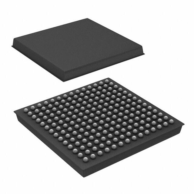
196-Ball, 15-mm × 15-mm NFBGA, 1-mm Pitch
2 Applications
•
•
•
•
Optical Switches
Optical Attenuators
Automatic Test Equipment (ATE)
Instrumentation
Communication to the device is performed through a
high-speed, 4-wire, serial interface compatible with
industry
standard
microprocessors
and
microcontrollers.
The DAC60096 can be set up to clear or update all
DACs simultaneously. In addition, a versatile external
conversion trigger allows each DAC channel to
operate as a square-wave generator with
independent amplitude control.
The DAC60096 is characterized for operation over
the temperature range of –40°C to +85°C, and is
available in a 196-ball, 15-mm × 15-mm, 1-mm pitch,
BGA package.
Device Information(1)
PART NUMBER
PACKAGE
DAC60096
NFBGA
BODY SIZE (NOM)
15.0 mm × 15.0 mm
(1) For all available packages, see the package option addendum
at the end of the data sheet.
Typical Application
2.5-V
Reference
RESET
Power-On
Reset
DAC60096
10.5 V
10.5 V
±10.5 V
±10.5 V
CS
SCLK
SDI
SDO
LDAC
CLEAR
STATS
Data
Buffer 1A
Data
Buffer 1B
Data
Register 1A
DAC1
Data
Register 1B
Control Logic
Processor
SPI Interface
Subsystem 1
Channel 1
Channel 13
Channel 24
TRIGG
Subsystem 2
Optical
Component
Subsystem 3
Subsystem 4
DVDD
AVCC
AVSS
3.3 V
12 V
±12 V
AGND
DGND REFGND
1
An IMPORTANT NOTICE at the end of this data sheet addresses availability, warranty, changes, use in safety-critical applications,
intellectual property matters and other important disclaimers. PRODUCTION DATA.
�DAC60096
SBAS721A – DECEMBER 2015 – REVISED JANUARY 2016
www.ti.com
Table of Contents
1
2
3
4
5
6
Features ..................................................................
Applications ...........................................................
Description .............................................................
Revision History.....................................................
Pin Configuration and Functions .........................
Specifications.........................................................
6.1
6.2
6.3
6.4
6.5
6.6
6.7
6.8
6.9
6.10
6.11
7
1
1
1
2
3
6
Absolute Maximum Ratings ...................................... 6
ESD Ratings.............................................................. 6
Recommended Operating Conditions....................... 6
Thermal Information .................................................. 7
Electrical Characteristics: DAC DC........................... 7
Electrical Characteristics: Square-Wave Output....... 8
Electrical Characteristics: General ............................ 9
Timing Requirements .............................................. 10
Typical Characteristics: DC Mode........................... 12
Typical Characteristics: Toggle Mode................... 14
Typical Characteristics, General ........................... 15
Detailed Description ............................................ 18
7.1 Overview ................................................................. 18
7.2 Functional Block Diagram ....................................... 18
7.3
7.4
7.5
7.6
8
Feature Description.................................................
Device Functional Modes........................................
Programming ..........................................................
Register Maps ........................................................
19
22
23
25
Application and Implementation ........................ 31
8.1 Application Information............................................ 31
8.2 Typical Application ................................................. 32
9
Power Supply Recommendations...................... 36
9.1 Device Reset Options ............................................. 36
10 Layout................................................................... 38
10.1 Layout Guidelines ................................................. 38
10.2 Layout Examples................................................... 38
11 Device and Documentation Support ................. 45
11.1
11.2
11.3
11.4
11.5
Documentation Support .......................................
Community Resources..........................................
Trademarks ...........................................................
Electrostatic Discharge Caution ............................
Glossary ................................................................
45
45
45
45
45
12 Mechanical, Packaging, and Orderable
Information ........................................................... 45
4 Revision History
Changes from Original (December 2015) to Revision A
•
2
Page
Changed from product preview to production data ................................................................................................................ 1
Submit Documentation Feedback
Copyright © 2015–2016, Texas Instruments Incorporated
Product Folder Links: DAC60096
�DAC60096
www.ti.com
SBAS721A – DECEMBER 2015 – REVISED JANUARY 2016
5 Pin Configuration and Functions
ZEB Package
196-Ball NFBGA
Top View
A
B
C
D
E
F
G
H
J
K
L
M
N
P
14
DAC14
G4
AVSS
G4
VREFL
G4
VREFH
G4
AVCC
G4
DNC
REF2
REF
GND2
DNC
AVCC
G5
VREFH
G5
VREFL
G5
AVSS
G5
DAC13
G5
13
DAC15
G4
DAC17
G4
DAC20
G4
DAC21
G4
DAC22
G4
DAC24
G4
DAC2
G3
DAC3
G5
DAC5
G5
DAC6
G5
DAC7
G5
DAC8
G5
DAC10
G5
DAC12
G5
12
DAC16
G4
DAC18
G4
DAC19
G4
DAC23
G4
DAC4
G3
DAC3
G3
DAC1
G3
DAC4
G5
DAC24
G6
DAC23
G6
DAC21
G6
DAC9
G5
DAC19
G6
DAC11
G5
11
DAC10
G3
DAC8
G3
DAC6
G3
DAC5
G3
DAC24
G2
DNC
DNC
DNC
DNC
DAC1
G7
DAC22
G6
DAC20
G6
DAC18
G6
DAC17
G6
10
DAC11
G3
DAC9
G3
DAC7
G3
AGND
AGND
AGND
AGND
AGND
AGND
AGND
AGND
DAC5
G7
DAC7
G7
DAC16
G6
9
DAC12
G3
AVSS
G3
VREFL
G3
VREFH
G3
AVCC
G3
AVSS
S2
DGND
DGND
AVSS
S3
AVCC
G6
VREFH
G6
VREFL
G6
AVSS
G6
DAC15
G6
8
DAC13
G3
AVSS
G3
VREFL
G3
VREFH
G3
AVCC
G3
AVCC
S2
DVDD
DVDD
AVCC
S3
AVCC
G6
VREFH
G6
VREFL
G6
AVSS
G6
DAC14
G6
7
DAC14
G2
AVSS
G2
VREFL
G2
VREFH
G2
AVCC
G2
AVCC
S1
DVDD
DVDD
AVCC
S4
AVCC
G7
VREFH
G7
VREFL
G7
AVSS
G7
DAC13
G7
6
DAC15
G2
AVSS
G2
VREFL
G2
VREFH
G2
AVCC
G2
AVSS
S1
DGND
DGND
AVSS
S4
AVCC
G7
VREFH
G7
VREFL
G7
AVSS
G7
DAC12
G7
5
DAC16
G2
DAC17
G2
DAC20
G2
DAC21
G2
DAC22
G2
AGND
AGND
CLEAR
AGND
DAC3
G7
DAC4
G7
DAC6
G7
DAC9
G7
DAC11
G7
4
DAC10
G1
DAC7
G1
DAC19
G2
DAC23
G2
DAC1
G1
RESET
CS
SCLK
LDAC
DAC2
G7
DAC25
G8
DAC21
G8
DAC8
G7
DAC10
G7
3
DAC11
G1
DAC8
G1
DAC18
G2
DAC3
G1
DAC2
G1
STATS
SDO
SDI
TRIGG
DAC26
G8
DAC24
G8
DAC19
G8
DAC17
G8
DAC16
G8
2
DAC12
G1
DAC9
G1
DAC6
G1
DAC5
G1
DAC4
G1
AGND
AGND
AGND
AGND
DAC23
G8
DAC22
G8
DAC20
G8
DAC18
G8
DAC15
G8
1
DAC13
G1
AVSS
G1
VREFL
G1
VREFH
G1
AVCC
G1
AGND
REF1
REF
GND1
AGND
AVCC
G8
VREFH
G8
VREFL
G8
AVSS
G8
DAC14
G8
DAC Output
Subsystem 1
Digital I/O
AVCC
DAC Output
Subsystem 2
Reference
Inputs (2.5 V)
AVSS
DAC Output
Subsystem 3
Reference
Compensation
DVDD
DAC Output
Subsystem 4
Do Not Connect
Ground
Submit Documentation Feedback
Copyright © 2015–2016, Texas Instruments Incorporated
Product Folder Links: DAC60096
3
�DAC60096
SBAS721A – DECEMBER 2015 – REVISED JANUARY 2016
www.ti.com
Pin Functions
PIN
TYPE
DESCRIPTION
NAME
NO.
AGND
D10, E10,
F1, F2, F5, F10,
G2, G5, G10, H2, H10,
J1, J2, J5, J10,
K10, L10
GND
Analog ground.
AVCC
E1, E6, E7, E8, E9, E14,
F7, F8, J7, J8,
K1, K6, K7, K8, K9, K14
PWR
Positive analog supply voltage. (11.2 V to 12.6 V). A 100-nF bypass capacitor for each AVCC_n (n
= G1, G2, G3, G4, G5, G6, G7, G8, S1, S2, S3 or S4) is required; place as close as possible to the
pins.
AVSS
B1, B6, B7, B8, B9, B14,
F6, F9, J6, J9,
N1, N6, N7, N8, N9, N14
PWR
Negative analog supply voltage. (-12.6V to -11.2V). A 100-nF bypass capacitor for each AVSS_n (n
= G1, G2, G3, G4, G5, G6, G7, G8, S1, S2, S3 or S4) is required; place as close as possible to the
pins.
H5
I
Asynchronous clear control input, active low. When CLEAR is low, all DACs are loaded with code
000h. When CLEAR is high, all DACs return to normal operation
Serial data enable, active low. This input is the frame synchronization signal for the serial data.
CLEAR
CS
G4
I
DAC[1-13]_G1
A1, A2, A3, A4,
B2, B3, B4, C2, D2, D3,
E2, E3, E4
O
DAC[14-26]_G2
A5, A6, A7, B5,
C3, C4, C5,
D4, D5, E5, E11
O
DAC[1-13]_G3
A8, A9, A10, A11,
B10, B11, C10, C11,
D11, E12, F12, G12, G13
O
DAC[14-24]_G4
A12, A13, A14,
B12, B13, C12, C13,
D12, D13, E13, F13
O
DAC[3-13]_G5
H12, H13, J13, K13, L13,
M12, M13, N13,
P12, P13, P14
O
DAC[14-26]_G6
J12, K12
L11, L12, M11, N11, N12,
P8, P9, P10, P11
O
DAC[1-13]_G7
K4, K5, K11, L5,
M5, M10, N4, N5, N10,
P4, P5, P6, P7
O
DAC[14-26]_G8
K2, K3, L2, L3, L4,
M2, M3, M4, N2, N3,
P1, P2, P3
O
DGND
G6, G9, H6, H9
GND
DNC
F11, F14, G11
H11, J11, J14
—
DVDD
G7, G8, H7, H8
PWR
LDAC
J4
I
Synchronous DAC load control input, active low. When LDAC is low, the DAC outputs are updated
immediately after a register write. If left high during DAC register updates, bringing LDAC low
causes all DAC outputs to update simultaneously.
RESET
F4
I
Reset input, active low. Logic low on this pin causes the device to perform a hardware reset.
REFGND1
H1
GND
Reference ground. Ground reference point for REF1. REFGND1 should be star connected at the
system GND source and not connected to the GND plane for best performance.
REFGND2
H14
GND
Reference ground. Ground reference point for REF2. REFGND2 should be star connected at the
system GND source and not connected to the GND plane for best performance.
SCLK
H4
I
Serial interface clock.
SDI
H3
I
Serial interface data input. Data are clocked into the input shift register on each rising edge of
SCLK.
SDO
G3
O
Serial interface data output. The SDO pin is in high impedance when CS is high. Data can be
clocked out of the input shift register on either rising or falling edges of SCLK as specified by
PHAINV in the CON register.
STATS
F3
O
DAC output status indicator. Identifies which of the two DAC data registers is active.
REF1
G1
I
Input voltage reference pin 1 (2.5 V). A 100-nF bypass capacitor between this pin and REFGND1 is
required.
REF2
G14
I
Input voltage reference pin 2 (2.5 V). A 100-nF bypass capacitor between this pin and REFGND2 is
required.
4
Subsystem 1 Regular DAC outputs: DAC group 1 and DAC group 2. Each DAC subsystem can be
controlled independently through the serial interface.
Subsystem 2 Regular DAC outputs: DAC group 3 and DAC group 4. Each DAC subsystem can be
controlled independently through the serial interface.
Subsystem 3 Regular DAC outputs: DAC group 5 and DAC group 6. Each DAC subsystem can be
controlled independently through the serial interface.
Subsystem 4 Regular DAC outputs: DAC group 7 and DAC group 8. Each DAC subsystem can be
controlled independently through the serial interface.
Digital ground. Ground reference point for all digital circuitry on the device.
Reserved for factory use. For proper operation, do not connect.
Digital supply voltage. (3 V to 5.5 V). A 100-nF bypass capacitor is required; place as close as
possible to the pins.
Submit Documentation Feedback
Copyright © 2015–2016, Texas Instruments Incorporated
Product Folder Links: DAC60096
�DAC60096
www.ti.com
SBAS721A – DECEMBER 2015 – REVISED JANUARY 2016
Pin Functions (continued)
PIN
TYPE
DESCRIPTION
NAME
NO.
TRIGG
J3
I
Trigger input signal. Enables all DAC outputs to toggle between the two DAC data registers
associated with each DAC. This functionality enables the device to operate as a square-wave
generator. The DAC registers are prepared for toggle mode operation on a TRIGG rising edge and
the outputs are toggled on each following TRIGG falling edge.
VREFH
D1, D6, D7, D8, D9, D14,
L1, L6, L7, L8, L9, L14
O
Compensation capacitor connection for the internal 10.5 V reference voltage. A 100-nF bypass
capacitor for each VREFH_n (n = G1, G2, G3, G4, G5, G6, G7 or G8) is required; place as close as
possible to the pins.
VREFL
C1, C6, C7, C8, C9, C14,
M1, M6, M7, M8, M9, M14
O
Compensation capacitor connection for the internal -10.5 V reference voltage. A 100-nF bypass
capacitor for each VREFL_n (n = G1, G2, G3, G4, G5, G6, G7 or G8) is required; place as close as
possible to the pins.
Submit Documentation Feedback
Copyright © 2015–2016, Texas Instruments Incorporated
Product Folder Links: DAC60096
5
�DAC60096
SBAS721A – DECEMBER 2015 – REVISED JANUARY 2016
www.ti.com
6 Specifications
6.1 Absolute Maximum Ratings
over operating free-air temperature range (unless otherwise noted) (1)
MIN
MAX
–0.3
13
AVSS to DGND
–13
0.3
DVDD to DGND
–0.3
6
AVCC to AVSS
–0.3
26
DGND to AGND
–0.3
0.3
DGND to REFGND[1,2]
–0.3
0.3
REF1 to REFGND1
–0.3
6
AVCC to DGND
Supply voltage
REF2 to REFGND2
–0.3
6
AVCC + 0.3
–0.3
DVDD + 0.3
VREFH to DGND
–0.3
AVCC + 0.3
VREFL to DGND
AVSS – 0.3
0.3
VREFH to adjacent VREFL
–0.3
26
Operating, TA
–40
85
Junction, TJ
–40
150
Storage, Tstg
–40
150
CLEAR, CS, LDAC, RESET, SCLK, SDI, SDO, TRIGG,
STATS to DGND
Temperature
(1)
V
AVSS – 0.3
DAC to DGND
Pin voltage
UNIT
V
°C
Stresses beyond those listed under Absolute Maximum Ratings may cause permanent damage to the device. These are stress ratings
only, which do not imply functional operation of the device at these or any other conditions beyond those indicated under Recommended
Operating Conditions. Exposure to absolute-maximum-rated conditions for extended periods may affect device reliability.
6.2 ESD Ratings
VALUE
V(ESD)
(1)
(2)
Electrostatic discharge
Human-body model (HBM), per ANSI/ESDA/JEDEC JS-001 (1)
±2000
Charged-device model (CDM), per JEDEC specification JESD22-C101 (2)
±500
UNIT
V
JEDEC document JEP155 states that 500-V HBM allows safe manufacturing with a standard ESD control process.
JEDEC document JEP157 states that 250-V CDM allows safe manufacturing with a standard ESD control process.
6.3 Recommended Operating Conditions
over operating free-air temperature range (unless otherwise noted)
MIN
NOM
MAX
UNIT
POWER SUPPLY
AVCC
11.2
12
12.6
V
AVSS
–12.6
–12
–11.2
V
3
3.3
5.5
V
22.4
24
25.2
V
DVDD
V
2.525
V
85
°C
DVDD
AVCC to AVSS
DIGITAL INPUTS
Digital input voltage
0
REFERENCE INPUT
Reference input voltage, VREF
2.475
2.5
TEMPERATURE
Operating ambient temperature, TA
6
–40
Submit Documentation Feedback
Copyright © 2015–2016, Texas Instruments Incorporated
Product Folder Links: DAC60096
�DAC60096
www.ti.com
SBAS721A – DECEMBER 2015 – REVISED JANUARY 2016
6.4 Thermal Information
DAC60096
THERMAL METRIC (1)
ZEB (NFBGA)
UNIT
196 BALLS
RθJA
Junction-to-ambient thermal resistance
21.4
°C/W
RθJC(top)
Junction-to-case (top) thermal resistance
7.5
°C/W
RθJB
Junction-to-board thermal resistance
5.1
°C/W
ψJT
Junction-to-top characterization parameter
0.4
°C/W
ψJB
Junction-to-board characterization parameter
5.0
°C/W
RθJC(bot)
Junction-to-case (bottom) thermal resistance
N/A
°C/W
(1)
For more information about traditional and new thermal metrics, see the Semiconductor and IC Package Thermal Metrics application
report, SPRA953.
6.5 Electrical Characteristics: DAC DC
at AVCC = 11.2 V to 12.6 V, AVSS = –12.6 V to –11.2 V, DVDD = 3 V to 5.5 V, AGND = DGND = REFGND[1,2] = 0 V, REF1 =
REF2 = 2.5 V (specifications exclude any reference contributions), no load on DACs, and TA = –40°C to +85°C (unless
otherwise noted)
PARAMETER
TEST CONDITIONS
MIN
TYP
MAX
UNIT
±0.15
±1
LSB
±0.1
±0.9
LSB
±0.05
±0.15
%FSR
±2
±7
STATIC PERFORMANCE
Resolution
12
INL
Relative accuracy
DNL
Differential nonlinearity
Specified 12-bit monotonic
Gain error
TA = 25°C
Zero-code error
TA = 25°C, code 000h
Bits
mV
Gain error drift
±1
ppm/°C
Zero-code error drift
±1
ppm/°C
OUTPUT CHARACTERISTICS
Output voltage
–10.5
Output impedance
DC crosstalk
Settling time
Output noise
10.5
V
41
kΩ
Measured channel at code 000h, all
others transition from code 7FFh to 02Bh
0.5
LSB
DAC ouput transition:
code 800h to 7FFh to within 1 LSB,
6x load:
R(SERIES) = 17 kΩ, CLOAD = 300 pF
160
DAC ouput transition:
code 800h to 7FFh to within 1 LSB,
1x load:
R(SERIES) = 100 kΩ, CLOAD = 50 pF
65
TA = 25°C, 1 kHz, code 000h
60
µs
nV/√Hz
Submit Documentation Feedback
Copyright © 2015–2016, Texas Instruments Incorporated
Product Folder Links: DAC60096
7
�DAC60096
SBAS721A – DECEMBER 2015 – REVISED JANUARY 2016
www.ti.com
6.6 Electrical Characteristics: Square-Wave Output
at AVCC = 11.2 V to 12.6 V, AVSS = –12.6 V to –11.2 V, DVDD = 3 V to 5.5 V, AGND = DGND = REFGND[1,2] = 0 V, REF1 =
REF2 = 2.5 V (specifications exclude any reference contributions), no load on DACs, and TA = –40°C to +85°C (unless
otherwise noted)
PARAMETER
TEST CONDITIONS
MIN
TYP
MAX
UNIT
DAC OUTPUTS – 6x LOAD: R(SERIES) = 17 kΩ, CLOAD = 300 pF
Frequency
Amplitude
Amplitude step precision
Amplitude temperature drift
Offset voltage
Rise and fall time
For amplitude ≥ 9.1 VRMS, amplitude = ±10.5 VPP,
codes 7FFh to 801h
Amplitude
Amplitude step precision
Amplitude temperature drift
Offset voltage
Rise and fall time
(1)
8
kHz
Frequency = 3 kHz, amplitude = ±10.5 VPP,
codes 7FFh to 801h
9.1
VRMS
Frequency = 5 kHz, amplitude = ±10.5 VPP,
codes 7FFh to 801h
8
VRMS
Frequency = 3 kHz, amplitude ≥ 1 VRMS
6
mVRMS
Frequency = 3 kHz, amplitude = ±5 VPP,
codes 3CFh to C31h
5
mVRMS
15
mVRMS
Frequency = 3 kHz, amplitude = ±10.5 VPP,
codes 7FFh to 801h
Frequency = 3 kHz, amplitude = ±5 VPP,
codes 3CFh to C31h
–10
10
mV
Frequency = 3 kHz, amplitude = ±10.5 VPP,
codes 7FFh to 801h
–10
10
mV
Frequency = 3 kHz, amplitude = ±10.5 VPP,
10% to 90%, codes 7FFh to 801h
DAC OUTPUTS – 1x LOAD: R(SERIES) = 100 kΩ, CLOAD = 50 pF
Frequency
3
40
µs
5
kHz
(1)
For amplitude ≥ 9.1 VRMS, amplitude = ±10.5 VPP,
codes 7FFh and 801h
Frequency = 3 kHz, amplitude = ±10.5 VPP,
codes 7FFh to 801h
10
VRMS
Frequency = 5 kHz, amplitude = ±10.5 VPP,
codes 7FFh to 801h
9.5
VRMS
Frequency = 3 kHz, amplitude ≥ 1 VRMS
7
mVRMS
Frequency = 3 kHz, amplitude = ±5 VPP,
codes 3CFh to C31h
5
mVRMS
15
mVRMS
Frequency = 3 kHz, amplitude = ±10.5 VPP,
codes 7FFh to 801h
Frequency = 3 kHz, amplitude = ±5 VPP,
codes 3CFh to C31h
–10
10
mV
Frequency = 3 kHz, amplitude = ±10.5 VPP,
codes 7FFh to 801h
–10
10
mV
Frequency = 3 kHz, amplitude = ±10.5 VPP,
10% to 90%, codes 7FFh to 801h
10
µs
Specified by design and characterization. Not tested during production.
Submit Documentation Feedback
Copyright © 2015–2016, Texas Instruments Incorporated
Product Folder Links: DAC60096
�DAC60096
www.ti.com
SBAS721A – DECEMBER 2015 – REVISED JANUARY 2016
6.7 Electrical Characteristics: General
at AVCC = 11.2 V to 12.6 V, AVSS = –12.6 V to –11.2 V, DVDD = 3 V to 5.5 V, AGND = DGND = REFGND[1,2] = 0 V, REF1 =
REF2 = 2.5 V (specifications exclude any reference contributions), no load on DACs, and TA = –40°C to +85°C (unless
otherwise noted)
PARAMETER
TEST CONDITIONS
MIN
TYP
MAX
2.475
2.5
2.525
UNIT
EXTERNAL REFERENCE INPUTS
VREF
Input voltage range
REF1 and REF2 input pins
Reference input current
Per input pin
1
V
µA
DIGITAL LOGIC
VIH
High-level input voltage
VIL
Low-level input voltage
0.7 × DVDD
VOH
High-level output voltage
ILOAD = 1 mA, SDO2x = 01
VOL
Low-level output voltage
ILOAD = –1 mA, SDO2x = 01
DVDD - 0.2
AVCC supply current
I(AVSS)
AVSS supply current
I(DVDD)
DVDD supply current
Power consumption
I(AVCC)
AVCC supply current
I(AVSS)
AVSS supply current
I(DVDD)
DVDD supply current
Power consumption
I(AVCC)
AVCC supply current
I(AVSS)
AVSS supply current
I(DVDD)
DVDD supply current
Power consumption
(2)
20
V
pF
(1)
I(AVCC)
(1)
V
V
0.4
Input capacitance
POWER REQUIREMENTS
V
0.3 × DVDD
18.1
6x load:
R(SERIES) = 17 kΩ, CLOAD = 300 pF
frequency = 3 kHz
48 DAC outputs, codes 7FFh and 801h
48 DAC outputs, codes 117h and EE9h
1x load:
R(SERIES) = 100 kΩ, CLOAD = 50 pF
frequency = 3 kHz
48 DAC outputs, codes 7FFh and 801h
48 DAC outputs, codes 117h and EE9h
–25
25
–18.1
2
mA
10
440
17
–22
(2)
6x load:
R(SERIES) = 17 kΩ, CLOAD = 300 pF
frequency = 3 kHz
All DAC outputs, codes 02Bh and FD5h
22
25
mA
mA
10
415
–30
mA
mW
–17
2
mA
mA
mW
30
–25
mA
mA
2
10
mA
650
760
mW
Power requirements tested unloaded during production. Load current contribution to power consumption specified by design and
characterization.
Specified by design and characterization. Not tested during production.
Submit Documentation Feedback
Copyright © 2015–2016, Texas Instruments Incorporated
Product Folder Links: DAC60096
9
�DAC60096
SBAS721A – DECEMBER 2015 – REVISED JANUARY 2016
www.ti.com
6.8 Timing Requirements (1) (2)
at AVCC = 11.2 V to 12.6 V, AVSS = –12.6 V to –11.2 V, DVDD = 3 V to 5.5 V, AGND = DGND = REFGND[1,2] = 0 V, REF1 =
REF2 = 2.5 V (specifications exclude any reference contributions), no load on DACs, and TA = –40°C to +85°C (unless
otherwise noted)
MIN
NOM
MAX
UNIT
32
MHz
18
MHz
SERIAL INTERFACE – DEFAULT MODE: SDO2X = 01, PHAINV = 01
fSCLK
SCLK frequency
Write operation
Read operation
Write operation
14
ns
Read operation
26
ns
Write operation
14
ns
Read operation
26
ns
tPH
SCLK pulse width high
tPL
SCLK pulse width low
tSU
SDI setup
5
ns
tH
SDI hold
10
ns
tCSS
CS setup
10
ns
tCSH
CS hold
20
ns
tIAG
Inter-access gap
70
ns
tODZ
SDO driven to tri-state
Read operation
0
20
ns
tOZD
SDO tri-state to driven
Read operation
0
20
ns
tOD1
SDO output delay
Read operation
0
20
ns
Write operation
32
MHz
Read operation
32
MHz
SERIAL INTERFACE – FAST MODE: SDO2X = 10, PHAINV = 10
fSCLK
SCLK frequency
tPH
SCLK pulse width high
Write operation
14
ns
Read operation
14
ns
Write operation
14
ns
Read operation
14
ns
tPL
SCLK pulse width low
tSU
SDI setup
5
ns
tH
SDI hold
10
ns
tCSS
CS setup
10
ns
tCSH
CS hold
20
ns
tIAG
Inter-access gap
70
tODZ
SDO driven to tri-state
Read operation
0
20
ns
tOZD
SDO tri-state to driven
Read operation
0
20
ns
tOD2
SDO output delay
Read operation
0
20
ns
ns
DIGITAL LOGIC
tRESETDLY
Reset delay
tRESETWD
RESET pulse width
tLDACS
tLDACH
tTRIGH
Delay from power-on-reset to normal operation
100
250
µs
Delay from hardware reset to normal operation
10
50
µs
Delay from software reset to normal operation
10
50
µs
500
ns
LDAC setup
0
ns
LDAC hold
0
ns
TRIGG pulse width high
30
ns
tTRIGL
TRIGG pulse width low
30
ns
tSTADLY
STATS output delay
(1)
(2)
10
25
ns
Specified by design and characterization. Not tested during production.
SDO loaded with 10-pF load capacitance for SDO timing specifications.
Submit Documentation Feedback
Copyright © 2015–2016, Texas Instruments Incorporated
Product Folder Links: DAC60096
�DAC60096
www.ti.com
SBAS721A – DECEMBER 2015 – REVISED JANUARY 2016
tIAG
tCSH
tCSS
tODZ
CS
tPH
tPL
SCLK
Bit 23
SDI
tSU
Bit 1
Bit 0
tH
Z
Z
SDO
tOZD
Figure 1. Serial Interface Write Timing Diagram
tIAG
tCSH
tCSS
tODZ
CS
tPH
tPL
SCLK
Bit 16
Bit 23
SDI
tSU
tH
Z
Bit 15
SDO
PHAINV = µ01
Z
tOD1
tOZD
Z
Bit 0
Bit 15
SDO
PHAINV = µ10
Bit 0
Z
tOD2
Figure 2. Serial Interface Read Timing Diagram
tLDACH
tLDACS
CS
LDAC
tTRIGH
tTRIGL
TRIGG
STATS
tSTADLY
Figure 3. Digital Logic Timing Diagram
Submit Documentation Feedback
Copyright © 2015–2016, Texas Instruments Incorporated
Product Folder Links: DAC60096
11
�DAC60096
SBAS721A – DECEMBER 2015 – REVISED JANUARY 2016
www.ti.com
6.9 Typical Characteristics: DC Mode
1.0
1.0
0.8
0.8
0.6
0.6
0.4
0.4
0.2
0.2
INL (LSB)
DNL (LSB)
at AVCC = 12 V, AVSS = –12 V, DVDD = 3.3 V, AGND = DGND = REFGND[1,2] = 0 V, REF1 = REF2 = 2.5 V (specifications
exclude any reference contributions), no load on DACs, and TA = 25°C (unless otherwise noted)
0.0
±0.2
0.0
±0.2
±0.4
±0.4
±0.6
±0.6
±0.8
±0.8
±1.0
±2048 ±1536 ±1024 ±512
0
512
1024
1536
Code
±1.0
±2048 ±1536 ±1024 ±512
2048
Figure 4. Differential Linearity Error (DNL)
512
1024
1536
2048
C002
Figure 5. Integral Linearity Error (INL)
1.0
1.0
0.8
0.8
0.6
0.6
0.4
0.4
0.2
0.2
INL (LSB)
DNL (LSB)
0
Code
C001
0.0
±0.2
±0.4
0.0
±0.2
±0.4
±0.6
±0.6
Max DNL
±0.8
±1.0
±40
±15
10
35
60
TA (ƒC)
Max INL
±0.8
Min DNL
Min INL
±1.0
85
±40
±15
10
35
60
TA (ƒC)
C005
Figure 6. DNL vs Temperature
85
C006
Figure 7. INL vs Temperature
2.0
0.05
0.03
1.0
Gain Error (%FSR)
Zero-code Error (mV)
0.04
0.0
±1.0
0.02
0.01
0.00
±0.01
±0.02
±0.03
±0.04
±2.0
±0.05
±40
±15
10
35
60
TA (ƒC)
85
±40
C007
Figure 8. Zero-Code Error vs Temperature
12
Submit Documentation Feedback
±15
10
35
60
TA (ƒC)
85
C008
Figure 9. Gain Error vs Temperature
Copyright © 2015–2016, Texas Instruments Incorporated
Product Folder Links: DAC60096
�DAC60096
www.ti.com
SBAS721A – DECEMBER 2015 – REVISED JANUARY 2016
Typical Characteristics: DC Mode (continued)
at AVCC = 12 V, AVSS = –12 V, DVDD = 3.3 V, AGND = DGND = REFGND[1,2] = 0 V, REF1 = REF2 = 2.5 V (specifications
exclude any reference contributions), no load on DACs, and TA = 25°C (unless otherwise noted)
500
400
1500
Settling Time (µs)
'$& 2XWSXW 1RLVH Q9 ¥+]
2000
1000
500
300
200
100
0
0
10
100
1K
10K
100K
Frequency (Hz)
1M
200
Figure 10. DAC Output Noise vs Frequency
400
600
800
Capacitive Load (pF)
C011
1000
C012
Figure 11. Settling Time Amplitude vs Capacitive Load
Submit Documentation Feedback
Copyright © 2015–2016, Texas Instruments Incorporated
Product Folder Links: DAC60096
13
�DAC60096
SBAS721A – DECEMBER 2015 – REVISED JANUARY 2016
www.ti.com
6.10 Typical Characteristics: Toggle Mode
at AVCC = 12 V, AVSS = –12 V, DVDD = 3.3 V, AGND = DGND = REFGND[1,2] = 0 V, REF1 = REF2 = 2.5 V (specifications
exclude any reference contributions), no load on DACs, and TA = 25°C (unless otherwise noted)
12
10
1X Load
8
6X Load
6
4
8
Offset (mV)
Amplitude (VRMS)
10
6
4
0
0
4
0
±2
±4
Freq = 100 Hz
Freq = 1 kHz
Freq = 3 kHz
Freq = 5 kHz
2
2
±6
±8
±10
8
12
16
20
Load Multiplier (X)
0
2
4
6
8
10
Amplitude (VRMS)
C013
C015
1x load: R(SERIES) = 100 kΩ, CLOAD = 50 pF
Figure 12. Maximum Amplitude vs Capacitive Load
Figure 13. Offset vs Amplitude
5
10
2.5 VRMS
RMS
3
0
±1
2
0
±2
±2
±4
±3
±6
±4
±8
±5
±10
10
±15
35
9 VRMS
RMS
4
1
±40
5 VRMS
RMS
6
9 VRMS
RMS
2
2.5 VRMS
RMS
8
5 VRMS
RMS
Offset (mV)
Amplitude Drift (mVRMS)
4
60
85
TA (ƒC)
±40
2.5 VRMS
RMS
5 VRMS
RMS
6.0
9 VRMS
RMS
4.0
Offset (mV)
Amplitude Drift (mV)
C017
8.0
9 VRMS
RMS
0.2
85
Figure 15. Offset vs Temperature
5 VRMS
RMS
0.3
60
10.0
2.5 VRMS
RMS
0.4
35
TA (ƒC)
Figure 14. Amplitude Drift vs Temperature
0.5
0.1
0.0
±0.1
2.0
0.0
±2.0
±0.2
±4.0
±0.3
±6.0
±8.0
±0.4
±0.5
11.2
11.4
11.6
11.8
12.0
12.2
12.4
AVss and AVcc Voltage Magnitude (V)
12.6
±10.0
11.2
C020
Figure 16. Amplitude Drift vs Supply Voltage
14
10
±15
C016
Submit Documentation Feedback
11.4
11.6
11.8
12.0
12.2
12.4
AVss and AVcc Voltage Magnitude (V)
12.6
C021
Figure 17. Offset vs Supply Voltage
Copyright © 2015–2016, Texas Instruments Incorporated
Product Folder Links: DAC60096
�DAC60096
www.ti.com
SBAS721A – DECEMBER 2015 – REVISED JANUARY 2016
6.11 Typical Characteristics, General
at AVCC = 12 V, AVSS = –12 V, DVDD = 3.3 V, AGND = DGND = REFGND[1,2] = 0 V, REF1 = REF2 = 2.5 V (specifications
exclude any reference contributions), no load on DACs, and TA = 25°C (unless otherwise noted)
10
DAC A
DAC B
10
8
5
0
0
±2
-2
±4
-4
±6
SCLK Input (V)
2
2
DAC B Output (mV)
4
4
±8
4
10
3
0
2
±10
1
-10
0
0.5
1
1.5
±20
0
-8
±12
±30
±1
2
0
Time (ms)
150
10
6
6
Voltage (V)
10
2
±2
AVCC
AVSS
DVDD
REF(1,2)
DAC
±1
0
1
C025
2
±2
AVCC
AVSS
DVDD
REF(1,2)
DAC
±10
±14
2
3
4
5
6
7
8
±1
1
2
8
Voltage (V)
8
0
AVCC
AVSS
DVDD
REF(1,2)
DAC
±15
6
6
7
8
C027
0
AVCC
AVSS
DVDD
REF(1,2)
DAC
±15
0
2
4
5
Time (ms)
C028
6x load: R(SERIES) = 17 kΩ, CLOAD = 300 pF
Square-wave output: freq = 1 kHz, full-scale amplitude
5
±8
8
Time (ms)
4
Figure 21. Recommended Power-Down Sequence
15
±8
3
Time (ms)
Figure 20. Recommended Power-Up Sequence
4
0
C026
15
2
900
±6
Time (ms)
0
750
Figure 19. SPI to DAC Crosstalk
14
±14
600
Time (ns)
Figure 18. DAC to DAC Crosstalk
±10
450
All DACs with zero-code inputs
SCLK frequency = 1 MHz
14
±6
300
C024
DAC A: square-wave output, freq = 1 kHz, full-scale amplitude
DAC B: zero-code inputs
Voltage (V)
20
-6
±10
Voltage (V)
30
SCLK
DAC
6
6
DAC A Output (V)
6
8
DAC Output (mV)
12
7
C029
6x load: R(SERIES) = 17 kΩ, CLOAD = 300 pF
Square-wave output: freq = 1 kHz, full-scale amplitude
Figure 22. DVDD Collapse and Recover
Figure 23. AVCC Collapse and Recover
Submit Documentation Feedback
Copyright © 2015–2016, Texas Instruments Incorporated
Product Folder Links: DAC60096
15
�DAC60096
SBAS721A – DECEMBER 2015 – REVISED JANUARY 2016
www.ti.com
Typical Characteristics, General (continued)
at AVCC = 12 V, AVSS = –12 V, DVDD = 3.3 V, AGND = DGND = REFGND[1,2] = 0 V, REF1 = REF2 = 2.5 V (specifications
exclude any reference contributions), no load on DACs, and TA = 25°C (unless otherwise noted)
12
12
DAC
DAC
CLEAR
CLEAR
4
4
Voltage (V)
Voltage (V)
TRIGG
8
TRIGG
8
0
0
±4
±4
±8
±8
±12
±12
0
1
2
3
0
4
Time (ms)
1
2
3
4
Time (ms)
C030
C031
6x load: R(SERIES) = 17 kΩ, CLOAD = 300 pF
Square-wave output: freq = 1 kHz, full-scale amplitude
6x load: R(SERIES) = 17 kΩ, CLOAD = 300 pF
Square-wave output: freq = 1 kHz, full-scale amplitude
Figure 25. Clear State to Normal Transition
Figure 24. Normal to Clear State Transition
12
10.0
DAC
TRIGG
8
8.0
IDVDD Current (mA)
LDAC
Voltage (V)
4
0
±4
6.0
4.0
2.0
±8
0.0
±12
0
1
2
3
4
Time (ms)
3.0
3.5
4.0
4.5
5.0
5.5
DVDD
C032
6x load: R(SERIES) = 17 kΩ, CLOAD = 300 pF
Square-wave output: freq = 1 kHz, full-scale amplitude
C033
No DAC load
Square-wave output: freq = 3 kHz, full-scale amplitude
Figure 26. LDAC DAC Transition
Figure 27. DVDD Current Consumption
Unloaded Current/DAC (µA)
300
200
100
0
±100
±200
AVCC
AVSS
±300
±2048 ±1536 ±1024 ±512
0
512
1024
“ Code
No DAC load, DVDD = 3.3 V
Square-wave output: freq = 3 kHz
2048
C035
No DAC load, DC output, DVDD = 3.3 V
Figure 28. Unloaded AVCC/AVSS Current Consumption
16
1536
Figure 29. Unloaded AVCC/AVSS Current Consumption
Submit Documentation Feedback
Copyright © 2015–2016, Texas Instruments Incorporated
Product Folder Links: DAC60096
�DAC60096
www.ti.com
SBAS721A – DECEMBER 2015 – REVISED JANUARY 2016
Typical Characteristics, General (continued)
at AVCC = 12 V, AVSS = –12 V, DVDD = 3.3 V, AGND = DGND = REFGND[1,2] = 0 V, REF1 = REF2 = 2.5 V (specifications
exclude any reference contributions), no load on DACs, and TA = 25°C (unless otherwise noted)
250
0
Regular: 1 kHz
Load Current/DAC (µA)
Load Current/DAC (µA)
Regular: 3 kHz
200
Regular: 5 kHz
150
100
50
±50
±100
±150
Regular: 1 kHz
±200
Regular: 3 kHz
Regular: 5 kHz
0
±250
0
4
8
12
16
Load Multiplier (X)
20
0
4
1x load: R(SERIES) = 100 kΩ, CLOAD = 50 pF, DVDD = 3.3 V
Square-wave output, full-scale amplitude
Figure 30. AVCC Load Current Consumption
8
12
16
Load Multiplier (X)
C036
20
C037
1x load: R(SERIES) = 100 kΩ, CLOAD = 50 pF, DVDD = 3.3 V
Square-wave output, full-scale amplitude
Figure 31. AVSS Load Current Consumption
Submit Documentation Feedback
Copyright © 2015–2016, Texas Instruments Incorporated
Product Folder Links: DAC60096
17
�DAC60096
SBAS721A – DECEMBER 2015 – REVISED JANUARY 2016
www.ti.com
7 Detailed Description
7.1 Overview
The DAC60096 is a low-power, 96-channel, 12-bit, digital-to-analog converter (DAC). The device provides
±10.5-V unbuffered bipolar voltage outputs while maintaining extremely low-power operation and good linearity.
The device integrates dedicated reference buffers that enable operation from an external 2.5-V reference source.
The DAC60096 can be set up to clear or update all DACs simultaneously. In addition a versatile external
conversion trigger allows each DAC to operate as an amplitude-independent square-wave generator. The device
incorporates a reset circuit that ensures all DAC outputs power up and remain at zero scale prior to device
configuration.
The DAC60096 features simplify the design of systems requiring a high number of precise analog control signals
such as those found in optical communications switches and attenuators.
The DAC60096 is designed as four DAC subsystems. Each DAC subsystem is configured independently through
a high speed 4-wire serial interface compatible with industry standard microprocessors and microcontrollers. The
DAC60096 is characterized for operation over the temperature range of –40°C to +85°C, and is available in a
196-ball, 15-mm × 15-mm, 1-mm pitch BGA package.
7.2 Functional Block Diagram
TRIGG
LDAC
RESET
CLEAR
Power-On
Reset
Control Logic
VREFL VREFH
VREFH VREFL
(x6) REF1 REF2 (x6)
(x6)
STATS (x6)
CS
SCLK
SDI
SDO
SPI Interface
DAC60096
Subsystem 1
Data
Buffer 1A
Register 1A
Data
Data
Buffer 1B
Register 1B
DAC1
Data
Channel 1
Channel 2
Channel 3
DAC1_G1
DAC2_G1
DAC3_G1
Channel 11
Channel 12
Channel 13
DAC11_G1
DAC12_G1
DAC13_G1
DAC14_G2 ± DAC24_G2
Subsystem 2
DAC1_G3 ± DAC13_G3
DAC14_G4 ± DAC24_G4
Subsystem 3
DAC3_G5 ± DAC13_G5
DAC14_G6 ± DAC24_G6
Subsystem 4
DAC1_G7 ± DAC13_G7
DAC14_G8 ± DAC26_G8
DVDD
(u4)
18
AVCC
(u16)
AVSS
(u16)
AGND
(u17)
DGND REFGND
(u4)
(u2)
Submit Documentation Feedback
Copyright © 2015–2016, Texas Instruments Incorporated
Product Folder Links: DAC60096
�DAC60096
www.ti.com
SBAS721A – DECEMBER 2015 – REVISED JANUARY 2016
7.3 Feature Description
7.3.1 Digital-to-Analog Converters (DACs)
The DAC60096 is a 96-channel, 12-bit digital-to-analog converter (DAC) with integrated reference buffers. Each
DAC output consists of an R-2R ladder configuration as shown in Figure 32.
The DAC60096 includes reference buffers that enable bipolar DAC output voltages of ±10.5 V from a 2.5-V
reference source. The outputs of the reference buffers drive the R-2R ladders.
R
R
VOUT
2R
2R
2R
2R
2R
2R
2R
S0
S1
S8
E1
E2
E7
VREFH
VREFL
3-MSBs Decoded into
7 Equal Segments
9-Bit R-2R Ladder
Figure 32. R-2R Ladder Configuration
7.3.1.1 DAC Transfer Function
The DAC60096 integrates dedicated reference buffers that enable operation from an external 2.5-V reference
source. The reference buffers generate the voltages, VREFH and VREFL, required to drive the DAC R-2R
ladders.
10.5
VREFH = VREF x
2.5
(1)
(2)
VREFL = -1 x VREFH
where VREF is the reference input voltage at pins REF1 and REF2.
Input data are written to the individual DAC data registers in 12-bit twos complement format. After power-on or a
reset event, all DAC registers are set to zero scale. The DAC transfer function is given by Equation 3.
Code
VOUT =
x (VREFH - VREFL)
4096
(3)
where Code is the signed decimal equivalent of the binary code loaded to the DAC register and ranges from
-2048 to 2047 (See Table 1).
Table 1. DAC Data Format
DIGITAL CODE
SIGNED DECIMAL VALUE
DAC OUTPUT VOLTAGE (V)
0111 1111 1111
+2047
10.49487
0111 1111 1110
+2046
10.48975
0000 0000 0001
+1
0.005127
0000 0000 0000
0
0
1111 1111 1111
–1
–0.005127
1000 0000 0001
–2047
–10.49487
1000 0000 0000
–2048
–10.5
Submit Documentation Feedback
Copyright © 2015–2016, Texas Instruments Incorporated
Product Folder Links: DAC60096
19
�DAC60096
SBAS721A – DECEMBER 2015 – REVISED JANUARY 2016
www.ti.com
7.3.1.2 DAC Register Structure
Each DAC in the device incorporates two data registers: Register A and Register B. These two data registers
and the TRIGG pin enable toggle mode operation. Alternatively, if the TRIGG pin is left fixed the device is in DC
mode operation and only one of the data registers is used to control the DAC output (Register A by default).
Data written to the DAC data registers is initially stored in the DAC buffer registers. Transfer of data from the
DAC buffer registers to the active DAC registers can be set to happen immediately (asynchronous mode) or
initiated by an LDAC trigger (synchronous mode). After data are transferred to the DAC active registers, the DAC
outputs are updated. When the host reads from a DAC data register, the value held in the DAC buffer register is
returned (not the value held in the DAC active register).
The DAC update mode is determined by the status of the LDAC input pin. If the LDAC pin is held low the device
is in asynchronous mode. In asynchronous mode, a write to a DAC data register results in an immediate update
of the DAC active register and the corresponding output. If LDAC is held high, the device is in synchronous
mode. In synchronous mode, writing to a DAC data register does not automatically update the DAC output.
Instead, the update occurs only after an LDAC trigger occurs. An LDAC trigger is generated either through a
high-to-low transition on the LDAC pin in which case all 96 DACs update at the same time or by the self-clearing
LDAC bit in each of the four subsystems CON registers (address 0x4, bit 15) which enables synchronization of
all the DACs in the selected subsystem.
After the DAC outputs have been configured, a clear event enables the DACs to be loaded with zero-code while
retaining the previously programmed values, thus allowing the possibility to return to the voltage being output
before the clear event was issued. Note that the DAC data registers can be updated while the device is in clear
state allowing the DACs to output new values upon return to normal operation. When the device exits the clear
state the DAC outputs are immediately loaded with the data in the DAC active registers.
The device is set into clear state through the CLEAR pin. Setting the CLEAR pin low forces all 96 DACs into
clear state. Setting the CLEAR pin back high returns all DACs to normal operation. Alternatively, the CLRDAC
bits in each of the four subsystems CON registers (Address 0x4, bits [5:4]) can be used to enter or exit clear
state at a subsystem level.
Serial Interface
DAC Data Register
READ
WRITE
DAC
Buffer Register
A
DAC
Active Register
A
0x0000
(asynchronous mode)
12-Bit
DAC
DAC Output
LDAC Trigger
(Synchronous Mode)
Clear State
(Asynchronous Mode)
DAC
Buffer Register
B
DAC
Active Register
B
Toggle Mode
Figure 33. DAC60096 DAC Block Diagram
20
Submit Documentation Feedback
Copyright © 2015–2016, Texas Instruments Incorporated
Product Folder Links: DAC60096
�DAC60096
www.ti.com
SBAS721A – DECEMBER 2015 – REVISED JANUARY 2016
7.3.2 Reference Specifications
The DAC60096 integrates dedicated reference buffers that enable operation from an external 2.5-V reference
source. The reference buffers generate the ±10.5-V levels used to drive the DACs in the device. A 100-nF
bypass capacitor should be placed between the REF[1,2] input pins and REFGND[1,2]. Additionally a
compensation 100-nF bypass capacitor for each VREFH_n and VREFL_n pin (n = G1, G2, G3, G4, G5, G6, G7
or G8) is required and should be placed as close as possible to the pins.
REF[1,2]
100 nF
(Minimize
inductance to pin)
Reference
(2.5V)
REFGND[1,2]
C = 100nF
(Minimize
inductance to pin)
VREFH_n
+10.5V
DAC Reference
DAC1
12-b
C = 100nF
(Minimize
inductance to pin)
VREFL_n
-10.5V
DAC Reference
Figure 34. Reference Operation
Submit Documentation Feedback
Copyright © 2015–2016, Texas Instruments Incorporated
Product Folder Links: DAC60096
21
�DAC60096
SBAS721A – DECEMBER 2015 – REVISED JANUARY 2016
www.ti.com
7.4 Device Functional Modes
7.4.1 Toggle Mode
Each DAC in the device incorporates two DAC registers: Register A and Register B. The TRIGG pin is used to
switch the DAC outputs back and forth between the contents of the two DAC specific registers. The DAC
registers are prepared for trigger mode operation on a TRIGG rising edge and the outputs are toggled on each
following high-to-low transition. This feature enables the generation of 96 amplitude independent square-waves.
The device incorporates an auto-populate feature that simplifies register configuration in toggle mode. Autopopulate is enabled by the APB bits in the CON register (address 0x4, bits [1:0]). When auto-populate is
enabled, a Register A update automatically loads Register B with the negative value of the data written to A.
Although the Register B data can be modified by a direct register write, this update does not auto-populate the
Register A contents.
The STATS output pin is used to identify the active register. A logic-low is output for Register A and logic-high for
register B. The STATS pin is in high impedance mode by default and must be enabled by the SDRV bits in the
CON register for subsystem 1 (address 0x4, bits [9:8]). The SDRV bits in the other three subsystems should be
set to high impedance mode (default mode).The toggling rate of the STATS terminal is determined by the SDIV
register (address 0x9). The SDIV register should only be updated after a device reset and before configuring the
DAC outputs The STATS output pin toggles on every 2SDIV trigger pulse (SDIV = 0, 1, …, 6).
7.4.2 DC Mode
A fixed TRIGG pin puts the device in DC mode operation. In DC mode only one of the two DAC data registers is
used to control the DAC output. If no TRIGG rising edge is detected by the device after power-up, Register A is
by default the active register.
22
Submit Documentation Feedback
Copyright © 2015–2016, Texas Instruments Incorporated
Product Folder Links: DAC60096
�DAC60096
www.ti.com
SBAS721A – DECEMBER 2015 – REVISED JANUARY 2016
7.5 Programming
The DAC60096 is controlled through a flexible four-wire serial interface that is compatible with SPI type
interfaces used on many microcontrollers and DSP controllers. The interface provides read/write access to all
registers of the DAC60096.
For simplification of the register structure, communication to the device is done at a subsystem level through the
PTR global pointer register (address 0x6). Subsystem addressing is done through SID[1:0], where subsystem 1
is the default setting. Access to all other registers in the device will affect only the subsystem selected by SID.
The DAC pointer setting, DPTR[4:0], also in the PTR register allows access to the data registers (BUFA and
BUFB) for any of the DACs in the chosen subsystem.
Each serial interface access cycle is exactly 24 bits long. A frame is initiated by asserting the CS pin low. The
frame ends when the CS pin is deasserted high. The frame's first byte input to SDI is the instruction cycle which
identifies the request as a read or write, streaming or single, and the 4-bit address to be accessed. The following
bits in the frame form the data cycle. For all writes, data are clocked on the rising edge of SCLK. On read
access, data are clocked out on the SDO pin on either the falling edge or rising edge of SCLK according to the
PHAINV setting in each of the four subsystems CON registers (address 0x4, bits [7:6]).
Table 2. Serial Interface Cycle
Bit
Field
Description
23
R/W
Identifies the communication as a read or write command to the addressed
register.
R/W = 0 sets a write operation. R/W = 1 sets a read operation.
22
S
Identifies the communication as a streaming operation.
S = 0 is used for single command instructions. Bit = 1 is used for streaming
operation.
21:18
A[3:0]
Register address.
Specifies the register to be accessed during the read or write operation.
17:16
Reserved
Reserved. Set to zeros for proper operation.
15:0
D[15:0]
Data cycle bits.
If a write command, the data cycle bits are the values to be written to the
register with address A[3:0]
If a read command, the data cycle bits are don't care values.
CS
1
2
3
4
5
6
7
8
9
10
11
12
13
14
15
16
17
18
19
20
21
22
23
24
SCLK
SDI
R/W S=0
A3
A2
A1
A0
0
0
D15 D14 D13 D12 D11 D10
SDO
D9
D8
D7
D6
D5
D4
D3
D2
D1
D0
All Zeros
Figure 35. Serial Interface Write Bus Cycle
CS
1
2
3
4
5
6
7
8
9
10
11
12
13
14
15
16
17
18
19
20
21
22
23
24
SCLK
SDI
S=0
A3
A2
A1
A0
All Zeros
PHAINV = 01
SDO
All Zeros
D15 D14 D13
All D12
ZerosD11 D10
D9
D8
D7
D6
D5
D4
D3
D2
D1
D0
PHAINV = 10
SDO
All Zeros
D15 D14 D13 D12 D11 D10
D9
D8
D7
D6
D5
D4
D3
D2
D1
D0
Figure 36. Serial Interface Read Bus Cycle
Submit Documentation Feedback
Copyright © 2015–2016, Texas Instruments Incorporated
Product Folder Links: DAC60096
23
�DAC60096
SBAS721A – DECEMBER 2015 – REVISED JANUARY 2016
www.ti.com
In order to simplify write or read operations to multiple DACs in a subsystem, streaming mode is supported. In
streaming mode, multiple bytes of data can be written to or read from the DAC60096 without specifically
providing instructions for each byte and is implemented by continually holding the CS pin active and continuing to
shift new data in or old data out of the device.
The DAC60096 starts reading or writing data to the DAC data register selected by the PTR register and
automatically increments the DAC pointer (DPTR) as long as the CS pin is asserted. If the last DAC in the
chosen subsystem has been reached and the CS pin is still asserted, the data register for this DAC will be
overwritten with the new data.
CS
1
2
3
4
5
6
7
8
9
25
41
57
SCLK
DAC N
SDI
R/W S=1
A3
A2
A1
A0
0
0
DAC N+1
DAC N+2
DAC N+3
{D11 ± D0, 0, 0, 0, 0} {D11 ± D0, 0, 0, 0, 0} {D11 ± D0, 0, 0, 0, 0} {D11 ± D0, 0, 0, 0, 0}
All Zeros
SDO
Figure 37. Serial Interface Streaming Write Cycle
CS
1
2
3
4
5
6
7
8
9
25
41
57
SCLK
SDI
R/W S=1
A3
A2
A1
A0
0
0
DAC N
SDO
All Zeros
DAC N+1
DAC N+2
DAC N+3
{D11 ± D0, 0, 0, 0, 0} {D11 ± D0, 0, 0, 0, 0} {D11 ± D0, 0, 0, 0, 0} {D11 ± D0, 0, 0, 0, 0}
Figure 38. Serial Interface Streaming Read Cycle
7.5.1 Frame Error Checking
If the DAC60096 is used in a noisy environment, error checking can be used to check the integrity of the serial
interface data communication between the device and the host processor. The frame error checking scheme is
based on the CRC-CCITT-16 polynomial x16 + x12 + x5 + 1 (that is, 0x1021). The CRC register (address 0x5)
stores the CRC computation for each single-command or streaming serial interface data write. Reading the CRC
register resets its contents to 0xFFFF.
Only valid data cycles are included in the CRC computation. For single-command instructions CRC is calculated
and updated only after 16 data bits are received. If a data cycle is longer than 16 bits, the additional bits are not
included into the CRC calculation. For streaming commands CRC is calculated and updated on the multiple 16bit data cycles received. If the number of data bits received is not a multiple of 16, the modulo 16 bits are
discarded from the CRC calculation.
24
Submit Documentation Feedback
Copyright © 2015–2016, Texas Instruments Incorporated
Product Folder Links: DAC60096
�DAC60096
www.ti.com
SBAS721A – DECEMBER 2015 – REVISED JANUARY 2016
7.6 Register Maps
Communication to the DAC60096 is done at a subsystem level. Subsystem addressing is done through the
global pointer register, SID[1:0]. Each subsystem has 16 registers. Access to the data registers of any of the
DACs in the chosen subsystem is done through a DAC pointer, DPTR[4:0].
SUB-SYSTEM 4
SUB-SYSTEM 3
SUB-SYSTEM 2
Reg6
SID[1:0]
SUB-SYSTEM 1
DPTR[4:0]
Reg0
Reg0/1
DAC
Buffer
Register
A
DAC
Active
Register A
...DACn
0x0000
DAC2
(Asynchronous Mode)
12-Bit
DAC
DAC1
LDAC Trigger
(Synchronous Mode)
Reg4
Clear State
(Asynchronous Mode)
CON
Reg1
Reg5
CRC
DAC
Buffer
Register
B
Square-Wave
Mode
DAC
Active
Register
B
Reg7
SWR
Reg8
PWRM
Reg9
SDIV
Figure 39. Register Configuration
Table 3. Register Map
ADDRESS
REGISTER
TYPE
REGISTER SETUP
RESET
A3
A2
A1
A0
D15
D14
D13
D12
D11
D10
D9
D3
D2
D1
D0
BUFA
R/W
0000
0
0
0
0
BUFA
0
0
0
0
BUFB
R/W
0000
0
0
0
1
BUFB
0
0
0
0
RESERVED
--
0000
0
0
1
0
0
0
0
0
0
0
0
0
0
0
0
0
0
0
0
0
RESERVED
--
0000
0
0
1
1
0
0
0
0
0
0
0
0
0
0
0
0
0
0
0
CON
R/W
0555
0
1
0
0
LDAC
0
0
0
PHAINV
CLRDAC
0
1
CRC
R
FFFF
0
1
0
1
PTR
R
0000
0
1
1
0
0
0
0
0
0
SWR
R/W
0000
0
1
1
1
PWRM
R/W
CAFE
1
0
0
0
SDIV
R/W
0000
1
0
0
1
0
0
0
RESERVED
--
0000
SDO2x
D8
D7
SDRV
D6
D5
D4
0
APB
CRC
SID
0
0
0
0
DPTR
SWR
PWRM
0
0
0
0
0
0
0
0xA – 0xF
0
0
0
SDIV
------
Submit Documentation Feedback
Copyright © 2015–2016, Texas Instruments Incorporated
Product Folder Links: DAC60096
25
�DAC60096
SBAS721A – DECEMBER 2015 – REVISED JANUARY 2016
www.ti.com
7.6.1 8.5.1 BUFA Register (address = 0x0) [reset = 0x0000]
Figure 40. BUFA Register
15
14
13
12
11
10
3
2
9
8
1
0
BUFA
R/W
7
6
5
4
BUFA
R/W
RESERVED
R/W
LEGEND: R/W = Read/Write; R = Read only; -n = value after reset
Table 4. BUFA Register
Bit
Field
Type
Reset
Description
15:4
BUFA
R/W
0000
Double-buffer MSB aligned 12-bit data for DAC register A. The
specific DAC accessed by this register must be first set by the
subsystem address (SID) and DAC pointer (DPTR).
3:0
Reserved
R/W
0000
Not used
7.6.2 BUFB Register (address = 0x1) [reset = 0x0000]
Figure 41. BUFB Register
15
14
13
12
11
10
3
2
9
8
1
0
BUFB
R/W
7
6
5
4
BUFB
R/W
Reserved
R/W
LEGEND: R/W = Read/Write; R = Read only; -n = value after reset
Table 5. BUFB Register
26
Bit
Field
Type
Reset
Description
15:4
BUFB
R/W
0000
Double-buffer MSB aligned 12-bit data for DAC register B. The
specific DAC accessed by this register must be first set by the
subsystem address (SID) and DAC pointer (DPTR).
3:0
Reserved
R/W
0000
Not used
Submit Documentation Feedback
Copyright © 2015–2016, Texas Instruments Incorporated
Product Folder Links: DAC60096
�DAC60096
www.ti.com
SBAS721A – DECEMBER 2015 – REVISED JANUARY 2016
7.6.3 CON Register (address = 0x4) [reset = 0x0555]
Figure 42. CON Register
15
LDAC
R/W
14
7
6
PHAINV[1:0]
R/W
13
Reserved
R/W
12
5
4
11
10
9
SDO2x[1:0]
R/W
3
CLRDAC[1:0]
R/W
8
SDRV[1:0]
R/W
2
1
Reserved
R/W
0
APB[1:0]
R/W
LEGEND: R/W = Read/Write; R = Read only; -n = value after reset
Table 6. CON Register
Bit
Field
Type
Reset
Description
15
LDAC
R/W
0
Setting this bit to 1 issues an LDAC trigger at CS rising edge.
Self-clearing bit.
14:12
Reserved
R/W
000
Not used.
11:10
SDO2x[1:0]
R/W
01
SDO 1x/2x drive strength:
01: 1x (default)
10: 2x
Writing 00 or 11 has no effect
9:8
SDRV[1:0]
R/W
01
SDRV control STATS pin drive type:
01: Hi-Z. STATS pin is disabled (default)
10: CMOS Push-pull output. Should only be enabled for
subsystem 1.
Writing 00 or 11 has no effect
7:6
PHAINV[1:0]
R/W
01
PHAINV controls SDO output edge:
01: SCLK NegEdge (default)
10: SCLK PosEdge
Writing 00 or 11 has no effect
5:4
CLRDAC[1:0]
R/W
01
Clear DAC state control:
01: Normal operating state (default)
10: Clear DAC state
Writing 00 or 11 has no effect
3:2
Reserved
R/W
01
Reserved for factory use
1:0
APB[1:0]
R/W
01
Auto populate B:
01: Auto-populates BUFB with the negative value of BUFA after
each BUFA register write. Writing to BUFB has no auto-populate
effect (default)
10: Disable auto populate B feature
Writing 00 or 11 has no effect
Submit Documentation Feedback
Copyright © 2015–2016, Texas Instruments Incorporated
Product Folder Links: DAC60096
27
�DAC60096
SBAS721A – DECEMBER 2015 – REVISED JANUARY 2016
www.ti.com
7.6.4 CRC Register (address = 0x5) [reset = 0xFFF]
Figure 43. CRC Register
15
14
13
12
11
10
9
8
3
2
1
0
CRC[15:0]
R
7
6
5
4
CRC[15:0]
R
LEGEND: R/W = Read/Write; R = Read only; -n = value after reset
Table 7. CRC Register
Bit
15:0
X15
Field
Type
Reset
Description
CRC[15:0]
R
FFFF
Stores the CRC computation data for each SPI data write. CRC
includes stream writes. The address byte is not included in the
CRC computation.
Reading Reg CRC resets current CRC value to 0xFFFF. CRC is
calculated when CS is enabled and the data cycle contains a
multiple of 16 bits. The redundant data are not written into the
register.
CRC-CCITT polynomial is used x16 + x12 + x5 + 1, or in hex:
0x1021 with default 0xFFFF.
X14
X13
X12
X11
X10
X9
X8
X7
X6
X5
X4
X3
X2
X1
X0
Figure 44. CRC CCITT 16
28
Submit Documentation Feedback
Copyright © 2015–2016, Texas Instruments Incorporated
Product Folder Links: DAC60096
�DAC60096
www.ti.com
SBAS721A – DECEMBER 2015 – REVISED JANUARY 2016
7.6.5 PTR Register (address = 0x6) [reset = 0x0000]
Figure 45. PTR Register
15
14
13
Reserved
R/W
7
12
11
10
SID[1:0]
R/W
6
Reserved
R/W
5
9
8
1
0
Reserved
R/W
4
3
2
DPTR[4:0]
R/W
LEGEND: R/W = Read/Write; R = Read only; -n = value after reset
Table 8. PTR Register
Bit
Field
Type
Reset
Description
15:14
Reserved
R/W
00
Reserved for factory use
13:12
SID[1:0]
R/W
00
Subsystem address:
00: Subsystem 1
01: Subsystem 2
10: Subsystem 3
11: Subsystem 4
11:8
Reserved
R/W
0000
Not used
7:5
Reserved
R/W
000
Reserved for factory use
4:0
DPTR[4:0]
R/W
0000
DAC pointer
7.6.6 SWR Register (address = 0x7) [reset = 0x0000]
Figure 46. SWR Register
15
14
13
12
11
10
9
8
3
2
1
0
SWR
R/W
7
6
5
4
SWR
R/W
LEGEND: R/W = Read/Write; R = Read only; -n = value after reset
Table 9. SWR Register
Bit
Field
Type
Reset
Description
15:0
SWR
R/W
0000
Writing 0xA5A5 to this register generates a software reset on the
CS rising edge of the command for a subsystem. The software
reset is similar to a hardware reset, which resets all registers
and logic states.
Reading this register gives the hardware version of the
subsystem.
Submit Documentation Feedback
Copyright © 2015–2016, Texas Instruments Incorporated
Product Folder Links: DAC60096
29
�DAC60096
SBAS721A – DECEMBER 2015 – REVISED JANUARY 2016
www.ti.com
7.6.7 PWRM Register (address = 0x6) [reset = 0xCAFE]
Figure 47. PWRM Register
15
14
13
12
11
10
9
8
3
2
1
0
PWRM
R/W
7
6
5
4
PWRM
R/W
LEGEND: R/W = Read/Write; R = Read only; -n = value after reset
Table 10. PWRM Register
Bit
15:0
Field
Type
Reset
Description
PWRM
R/W
0000
DVDD Power Monitor:
After device power up, the PWRM register is 0xCAFE. Any
register write to PWRM sets PWRM to 0xABBA. PWRM is reset
to 0xCAFE after a DVDD collapse initiated POR event. Reading
PWRM with value 0xCAFE indicates power failure or
uninitialized value.
The system controller can monitor PWRM to check for active
power status. The device toggles the PWRM value after every
PWRM register read. If the current read value is 0xABBA, the
next read value will be 0xBAAB, and vice versa.
The PWRM register only monitors DVDD power failure. AVCC is
monitored by the analog reset circuit. When there is a power
failure on AVCC all the DACs in the device go into clear state.
7.6.8 SDIV Register (address = 0x9) [reset = 0x0000]
Figure 48. SDIV Register
15
14
13
12
11
10
9
8
3
2
1
SDIV
R/W
0
Reserved
R/W
7
6
5
Reserved
R/W
4
LEGEND: R/W = Read/Write; R = Read only; -n = value after reset
Table 11. SDIV Register
Bit
30
Field
Type
Reset
Description
15:3
Reserved
R/W
0000
Not Used
2:0
SDIV
R/W
000
Status signal toggle rate:
STATS pin toggling rate is controlled by SDIV register. SDIV is
valid between 0 and 6. The STATS pin toggles on every 2SDIV
trigger pulse.
The SDIV setting should only be updated after a device reset
and before configuring the DAC outputs.
Submit Documentation Feedback
Copyright © 2015–2016, Texas Instruments Incorporated
Product Folder Links: DAC60096
�DAC60096
www.ti.com
SBAS721A – DECEMBER 2015 – REVISED JANUARY 2016
8 Application and Implementation
NOTE
Information in the following applications sections is not part of the TI component
specification, and TI does not warrant its accuracy or completeness. TI’s customers are
responsible for determining suitability of components for their purposes. Customers should
validate and test their design implementation to confirm system functionality.
8.1 Application Information
The DAC60096 is a low-power, 96-channel, 12-bit, digital-to-analog converter (DAC). The device provides
unbuffered bipolar voltage outputs up to ±10.5 V.
This device is suitable for many applications involving multichannel bipolar DACs. Such applications include
multichannel variable optical attenuators, MEMS mirror control, and ATE level drivers.
Submit Documentation Feedback
Copyright © 2015–2016, Texas Instruments Incorporated
Product Folder Links: DAC60096
31
�DAC60096
SBAS721A – DECEMBER 2015 – REVISED JANUARY 2016
www.ti.com
8.2 Typical Application
C3
0.1µF
C7
C6
0.1µF
C8
C9
0.1µF
0.1µF
DVDD
C10
0.22µF
C12
0.22µF
C17
AVCC
C11
C16
DGND
SDI
SCLK
SDO
STATS
2
4
6
8
10
TSW-105-07-G-D
/LDAC
/CLEAR
/CS
/RESET
DGND
DGND
DGND
DGND
DGND
AGND
J11-2
J11-1
J11-16
J11-15
J11-12
J11-14
J11-24
J11-22
J11-25
J11-23
J11-26
J11-27
J11-28
J11-17
J11-19
J11-21
J11-18
J11-20
J11-13
J11-9
J11-8
J11-6
J11-11
J11-5
PWR_GND
DAC1_G7
DAC2_G7
DAC3_G7
DAC4_G7
DAC5_G7
DAC6_G7
DAC7_G7
DAC8_G7
DAC9_G7
DAC10_G7
DAC11_G7
DAC12_G7
DAC13_G7
DAC14_G8
DAC15_G8
DAC16_G8
DAC17_G8
DAC18_G8
DAC20_G8
DAC19_G8
DAC21_G8
DAC22_G8
DAC23_G8
DAC24_G8
DAC25_G8
DAC26_G8
K11
K4
K5
L5
M10
M5
N10
N4
N5
P4
P5
P6
P7
P1
P2
P3
N3
N2
M2
M3
M4
L2
K2
L3
L4
K3
J12-1
J12-2
J12-5
J12-6
J12-8
J12-9
J12-13
J12-18
J12-21
J12-19
J12-17
J12-28
J12-27
J12-26
J12-23
J12-22
J12-20
J12-14
J12-11
J12-12
J12-16
J12-15
J12-10
J14-21
J14-7
J14-3
J12-24
J14-4
J12-25
J14-9
J14-6
J14-8
J14-5
J14-2
J14-1
J14-14
J14-12
J14-10
J14-11
J14-13
J14-19
J14-16
J14-15
J14-20
J14-22
J14-17
J14-18
J14-23
LDAC
CLEAR
STATS
TRIGG
DVDD
J1
1
3
5
7
9
REFGND2
NC
DAC3_G5
DAC4_G5
DAC5_G5
DAC6_G5
DAC7_G5
DAC8_G5
DAC9_G5
DAC10_G5
DAC11_G5
DAC12_G5
DAC13_G5
DAC14_G6
DAC15_G6
DAC16_G6
DAC17_G6
DAC18_G6
DAC19_G6
DAC20_G6
DAC21_G6
DAC22_G6
DAC23_G6
DAC24_G6
NC
NC
TP1
J4
H5
F3
J3
G6
G9
H6
H9
REF_GND
REF_GND
REF2
U1A
DAC60096NZHR
J14
H13
H12
J13
K13
L13
M13
M12
N13
P12
P13
P14
P8
P9
P10
P11
N11
N12
M11
L12
L11
K12
J12
J11
H11
J2
142-0701-201
1
R1
R2
R3
R4
R5
10.0k
10.0k
10.0k
10.0k
100k
DVDD
DGND
/LDAC
/CLEAR
STATS
REF5025IDGK
PWR_GND
REFGND1
CS
SCLK
SDI
SDO
H14
REF1
RESET
G14
10µF
C42
0.1µF
4
GND
H1
F4
C41
1µF
3
TEMP
C40
G4
H4
H3
G3
NC
DNC
DNC
G1
C37
0.1µF
5
/CS
SCLK
SDI
SDO
6
VOUT
TRIM/NR
/RESET
8
1
VIN
0.15µF
C58
7
0.15µF
C39
0.1µF
0.15µF
C57
C38
10µF
0.15µF
U2
2
DVDD
DVDD
DVDD
DVDD
0.15µF
C56
G8
H7
H8
0.15µF
0.22µF
VREFL_G1
VREFL_G2
VREFL_G2
VREFL_G3
VREFL_G3
VREFL_G4
VREFL_G5
VREFL_G6
VREFL_G6
VREFL_G7
VREFL_G7
VREFL_G8
C36
C1
C6
C7
C8
C9
C48
C14
C49 M14
M8
M9
M6
C50 M7
M1
DGND
AVCC
DVDD
0.22µF
G7
C47
0.22µF
0.15µF
C33
0.22µF
C35
0.22µF
PWR_GND
C34
C55
0.22µF
PWR_GND REF_GND AGND
0.15µF
0.1µF
C46
C31
0.15µF
C54
C28
0.22µF
C30
0.22µF
C32
C29
0.15µF
0.1µF
C45
0.1µF
C53
C27
0.1µF
0.15µF
C24
0.1µF
C26
C44
C25
C23
0.1µF
PWR_GND
DGND
AVSS _G1
AVSS_G2
AVSS_G2
AVSS_G3
AVSS_G3
AVSS_G4
AVSS_G5
AVSS_G6
AVSS_G6
AVSS_G7
AVSS_G7
AVSS _G8
AVSS _S1
AVSS _S2
AVSS_S3
AVSS _S4
0.15µF
C52
0.15µF
0.1µF
0.15µF
C20
0.1µF
VREFH_G1
VREFH_G2
VREFH_G2
VREFH_G3
VREFH_G3
VREFH_G4
VREFH_G5
VREFH_G6
VREFH_G6
VREFH_G7
VREFH_G7
VREFH_G8
C22
1µF
B1
B6
B7
B8
B9
B14
N14
N8
N9
N6
N7
N1
F6
F9
J9
J6
AVSS
0.1µF
C19
AVSS
C21
10µF
0.22µF
D1
D6
D7
D8
D9
D14
L14
L8
L9
L6
L7
L1
PWR_GND
C18
0.22µF
C43
PWR_GND
0.1µF
0.15µF
C15
0.1µF
C51
C14
1µF
C13
10µF
0.1µF
0.15µF
DGND
0.1µF
AGND
AGND
AGND
AGND
AGND
AGND
AGND
AGND
AGND
AGND
AGND
AGND
AGND
AGND
AGND
AGND
AGND
C5
0.1µF
AVCC_G1
AVCC_G2
AVCC_G2
AVCC_G3
AVCC_G3
AVCC_G4
AVCC_G5
AVCC_G6
AVCC_G6
AVCC_G7
AVCC_G7
AVCC_G8
AVCC_S1
AVCC_S2
AVCC_S3
AVCC_S4
D10
E10
F1
F2
F5
F10
G2
G5
G10
H2
H10
J1
J2
J5
J10
K10
L10
C4
1µF
E1
E6
E7
E8
E9
E14
K14
K8
K9
K6
K7
K1
F7
F8
J8
J7
5
4
3
2
0.1µF
C2
DAC1_G3
DAC2_G3
DAC3_G3
DAC4_G3
DAC5_G3
DAC6_G3
DAC7_G3
DAC8_G3
DAC9_G3
DAC10_G3
DAC11_G3
DAC12_G3
DAC13_G3
DAC14_G4
DAC15_G4
DAC16_G4
DAC17_G4
DAC18_G4
DAC19_G4
DAC20_G4
DAC21_G4
DAC22_G4
DAC23_G4
DAC24_G4
NC
DAC1_G1
DAC2_G1
DAC3_G1
DAC4_G1
DAC5_G1
DAC6_G1
DAC7_G1
DAC8_G1
DAC9_G1
DAC10_G1
DAC11_G1
DAC12_G1
DAC13_G1
DAC14_G2
DAC15_G2
DAC16_G2
DAC17_G2
DAC18_G2
DAC19_G2
DAC20_G2
DAC21_G2
DAC22_G2
DAC23_G2
DAC24_G2
NC
NC
AVCC
C1
G12
G13
F12
E12
D11
C11
C10
B11
B10
A11
A10
A9
A8
A14
A13
A12
B13
B12
C12
C13
D13
E13
D12
F13
F14
E4
E3
D3
E2
D2
C2
B4
B3
B2
A4
A3
A2
A1
A7
A6
A5
B5
C3
C4
C5
D5
E5
D4
E11
G11
F11
J13-21
J13-23
J13-17
J13-22
J13-20
J13-19
J13-9
J13-11
J13-13
J13-8
J13-10
J13-12
J13-14
J13-1
J13-2
J13-5
J13-6
J13-16
J13-15
J13-4
J13-3
J13-7
J13-18
J11-10
An example schematic incorporating the DAC60096 device is shown in Figure 49.
PWR_GND
Figure 49. Example Schematic
32
Submit Documentation Feedback
Copyright © 2015–2016, Texas Instruments Incorporated
Product Folder Links: DAC60096
�DAC60096
www.ti.com
SBAS721A – DECEMBER 2015 – REVISED JANUARY 2016
8.2.1 Design Requirements
Figure 49 uses the parameters shown in Table 12.
Table 12. Design Parameters
PARAMETER
VALUE
AVCC
12 V
DVDD
5V
AVSS
–12 V
REF1
2.5 V
REF2
2.5 V
8.2.2 Detailed Design Procedure
The following sections display components and applications that may facilitate the design process.
8.2.2.1 Power-Supply Bypassing
For accurate, high-resolution performance, all power supply pins should be bypassed to ground with low ESR
ceramic bypass capacitors. For additional noise filtering, use a 10-µF capacitor in parallel with a 0.1-µF
capacitor.
8.2.2.2 Reference Input
The internal reference buffers of the DAC60096 device require an external 2.5-V reference voltage source, which
can be driven externally through a precision voltage source or generated from a high precision voltage IC. One
such integrated circuit is the REF5025, which is a low-noise, low-drift, high precision voltage reference. The basic
connections are listed in Figure 50. A supply bypass capacitor ranging between 1 µF to 10 µF is recommended.
A 1-µF to 50-µF output capacitor must be connected from VOUT to GND. The ESR value of the output capacitor
must be less than or equal to 1.5 Ω to ensure output stability. To help minimize noise, an additional 1-µF
capacitor is connected from TRIM/NR to GND.
AVCC
U2
2
C24
10µF
C26
0.1µF
7
8
1
PWR_GND
VIN
VOUT
TRIM/NR
NC
TEMP
DNC
DNC
GND
6
REFOUT
5
3
C28
1µF
C27
10µF
4
REF5025IDGK
REF_GND
Figure 50. External Reference
8.2.2.3 TRIGG/Signal Conditioning
The TRIGG input signal provides the square waveform required for the DAC60096 device to operate as a
square-wave generator. The DAC registers are prepared for square wave operation on a TRIGG rising edge and
the outputs toggle on the falling edge. The Timing Requirements (1) (2) table specifies the timing parameters
required for proper operation.
The TRIGG input signal can be supplied from a waveform generator or voltage-to-frequency converter. An
example device with schematic is provided in Figure 51. The device highlighted is the LM231, a precision
voltage-to-frequency converter with wide range of full-scale frequency (1 Hz to 100 kHz). In Figure 51 the device
is configured to display 0.05% linearity over an output frequency range of 10 Hz to 4 kHz with and input range of
25 mV to 12.5 V. For more information, refer to the Typical Applications section of the LM231 datasheet
(SNOSBI2).
(1)
(2)
Specified by design and characterization. Not tested during production.
SDO loaded with 10-pF load capacitance for SDO timing specifications.
Submit Documentation Feedback
Copyright © 2015–2016, Texas Instruments Incorporated
Product Folder Links: DAC60096
33
�DAC60096
SBAS721A – DECEMBER 2015 – REVISED JANUARY 2016
www.ti.com
DVDD
RS
5K Gain Adjust 12 kΩ
10 kΩ
U1
GND
THR
RIN
100 kΩ
VIN
CIN
0.1 μF
Vs
2
REF I
6
THR
FREQ OUT
3
I OUT
1
R/C
5
GND
4
7
COMP IN
8
VS
LM231AN
To DAC60096 TRIG Input
Freq_Out
THR
RL
100 kΩ
+Vs
22 kΩ
GND
Rt
6.8 kΩ
CL
1 μF
GND
Ct
0.01 μF
47 Ω
–Vs
(Optional) Offset Adjust
GND
fout = (VIN / 2.09 V) ´ (RS / RL) ´ (1 / (Rt ´ Ct))
GND
-All resistors 1% tolerance
-Caps with low dielectric absorption: NP0, C0G, polystyrene, and so on.
Figure 51. External Precision Voltage-to-Frequency Converter for TRIGG Signal
8.2.2.4 External Amplifier Selection
The outputs of the DAC60096 are unbuffered. The output impedance is specified as 41 kΩ. In applications
requiring an external buffer, the selected amplifier should exhibit both low-offset voltage and input bias current.
The input bias current of the amplifier creates a potential across the DAC output impedance. This voltage error is
equivalent to the input bias current multiplied by the DAC output impedance value. For fast settling, the slew rate
of the operational amplifier should not impede the settling time of the DAC. Output impedance of the DAC is
constant and code-independent, but in order to minimize gain errors the input impedance of the output amplifier
should be as high as possible. Additionally, the amplifier adds another time constant, which increases the settling
time response of the system. A higher 3-dB bandwidth amplifier effectively shortens the settling time, and
additionally increases the bandwidth of the system.
7
VCC
1
8
U1
OPA277U
6
2
3
5
Final Output
4
DACOUT
VSS
Figure 52. DAC Output With External Amplifier in Voltage-Follower Configuration
8.2.2.5 Unbuffered Settling Response
For applications that use the unbuffered output, the typical settling response for different capacitive loads is
displayed in Figure 53.
34
Submit Documentation Feedback
Copyright © 2015–2016, Texas Instruments Incorporated
Product Folder Links: DAC60096
�DAC60096
www.ti.com
SBAS721A – DECEMBER 2015 – REVISED JANUARY 2016
8.2.3 Application Curves
500
Settling Time (µs)
400
300
200
100
0
200
400
600
800
Capacitive Load (pF)
1000
C012
Figure 53. DAC Settling Time vs Capacitive Load
Submit Documentation Feedback
Copyright © 2015–2016, Texas Instruments Incorporated
Product Folder Links: DAC60096
35
�DAC60096
SBAS721A – DECEMBER 2015 – REVISED JANUARY 2016
www.ti.com
9 Power Supply Recommendations
It is highly recommended that AVCC is supplied prior to AVSS. DVDD sequencing is not critical. The recommended
sequence is AVCC followed by AVSS with DVDD and the REF[1,2] inputs applied last.
Table 13. Input-Voltage Recommendations
Supply voltage
MIN
TYP
MAX
UNIT
AVCC
11.2
12
12.6
V
AVSS
–12.6
–12
–11.2
V
DVDD
AVCC to AVSS
3
3.3
5.5
V
22.4
24
25.2
V
2.475
2.5
2.525
V
EXTERNAL REFERENCE INPUTS
VREF
Reference input voltage
REF1 and REF2 input pins
9.1 Device Reset Options
9.1.1 Power-on-Reset (POR)
The DAC60096 includes a power-on reset function. After the DVDD supply has been established a POR event is
issued. The POR causes all registers to initialize to their default values and communication with the device is
valid only after a 250 µs power-on-reset delay. The default value for all DACs is zero-code.
A power failure on DVDD also results in a power-on-reset event. The PWRM register (address 0x8) can be used
to monitor a DVDD power failure. After power-up the PWRM register is set to 0xCAFE. Any register write to the
PWRM register changes its contents to 0xABBA. If a PWRM register read returns 0xCAFE either the PWRM
register has not been initialized or a DVDD power failure has occured.
The device also includes an AVCC power failure detection circuit. In contrast to a DVDD power failure, a collapse
in AVCC does not result in a reset event. An AVCC power failure forces all DACs to go into clear state but does
not reset the DAC data register values which enables the device to return to normal operation once AVCC
recovers. Even though the DACs are loaded with zero-code during an AVCC power failure, it is important to note
that this does not necessarily indicate the DAC outputs will be at 0 V due to AVCC being outside of its supply
voltage range.
As long as DVDD and AVCC remain above their specified high threshold a power failure event will not occur. In
order to ensure a DVDD or AVCC collapse is registered as such by the device, these supplies must be below their
corresponding low threshold for at least 1 ms. When the supplies drop below their high threshold but remain over
the lower one (shown as the undefined region of Figure 54 and Figure 55), the device may or may not reset
(DVDD) or go into clear state (AVCC) under all specified temperature and power-supply conditions.
36
Submit Documentation Feedback
Copyright © 2015–2016, Texas Instruments Incorporated
Product Folder Links: DAC60096
�DAC60096
www.ti.com
SBAS721A – DECEMBER 2015 – REVISED JANUARY 2016
Device Reset Options (continued)
DVDD (V)
AVCC (V)
5.5
12.6
Specified Supply
Voltage Range
11.2
No Power-On Reset
Specified Supply
Voltage Range
Normal State
2.7
2.2
6
Undefined
Undefined
4
0.7
Power-On Reset
Clear State
0
0
Figure 54. Threshold Levels for DVDD POR Circuit
Figure 55. Threshold Levels for AVCC Clear Circuit
9.1.2 Hardware Reset
A device hardware reset event is initiated by a minimum 500 ns logic low on the RESET pin. A hardware reset
causes all registers to initialize to their default values and communication with the device is valid only after a 50
µs reset delay. The default value for all DACs is zero-code.
9.1.3 Software Reset
A subsystem software reset event is initiated by writing 0xA5A5 to the SWR register (address 0x7) for that
particular subsystem. The software reset command is triggered on the CS rising edge of the instruction. As with
the hardware reset, a software reset causes all registers to initialize to their default values and communication
with the device is valid only after a 50 µs. Note, however, that the reset only applies to the subsystem being
addressed during the command. In order to reset the entire device as a hardware reset does, a software reset
command should be issued to each of the four subsystems in the device.
Submit Documentation Feedback
Copyright © 2015–2016, Texas Instruments Incorporated
Product Folder Links: DAC60096
37
�DAC60096
SBAS721A – DECEMBER 2015 – REVISED JANUARY 2016
www.ti.com
10 Layout
10.1 Layout Guidelines
•
•
•
•
•
Bypass all power-supply pins to ground with a low ESR ceramic bypass capacitor. The typical recommended
bypass capacitance is 0.1-µF to 0.22-µF ceramic with a X7R or NP0 dielectric.
Place power supplies and VREFH/L bypass capacitors close to pins to minimize inductance and optimize
performance. Inner supply and reference pads can connect to the bypass arrangement on the bottom layer of
the PCB through vias to minimize trace length. This is illustrated in Figure 56 and Figure 59.
Include a 100-nF bypass capacitor for both internal reference inputs between this pin and their respective
ground pins.
Use a high-quality ceramic type NP0 or X7R for optimal performance across temperature, and low dissipation
factor.
Make sure that the digital and analog sections have proper placement with respect to the digital pins and
analog pins of the DAC60096 device. The separation of analog and digital blocks allow for better design and
practice because it reduces coupling into neighboring blocks, and minimizes the interaction between analog
and digital return currents.
10.2 Layout Examples
10.2.1 Optimal Layout Example
Optimal layout requires the addition of blind vias. This layout reduces trace length and brings the bypass
capacitor arrangements closer to the device pads. Figure 56 to Figure 59 show the board layouts.
38
Submit Documentation Feedback
Copyright © 2015–2016, Texas Instruments Incorporated
Product Folder Links: DAC60096
�DAC60096
www.ti.com
SBAS721A – DECEMBER 2015 – REVISED JANUARY 2016
Layout Examples (continued)
1
Pin 1
2
3 4
10 11 12 13
5
14
6 7 8
9
Place Bypass Capacitors
Close to Supply and
Reference Pins
1. 0.1uF
2. 0.15uF
3. 0.15uF
4. 0.1uF
5. 0.1uF
6. 0.1uF
7. 0.15uF
8. 0.15uF
9. 0.1uF
10. 0.1uF
11. 0.15uF
12. 0.15uF
13. 0.1uF
14. 0.1uF
15. 0.1uF
16. 0.15uF
17. 0.15uF
18. 0.1uF
15
16
17 18
Figure 56. DAC60096 Example Board Layout – Top Layer PCB
Submit Documentation Feedback
Copyright © 2015–2016, Texas Instruments Incorporated
Product Folder Links: DAC60096
39
�DAC60096
SBAS721A – DECEMBER 2015 – REVISED JANUARY 2016
www.ti.com
Layout Examples (continued)
AVCC
AVSS
Figure 57. DAC60096 Example Board Layout – Internal AVCC and AVSS Plane
40
Submit Documentation Feedback
Copyright © 2015–2016, Texas Instruments Incorporated
Product Folder Links: DAC60096
�DAC60096
www.ti.com
SBAS721A – DECEMBER 2015 – REVISED JANUARY 2016
Layout Examples (continued)
DVDD
Figure 58. DAC60096 Example Board Layout – DVDD Internal Plane With Select DAC Outputs
Submit Documentation Feedback
Copyright © 2015–2016, Texas Instruments Incorporated
Product Folder Links: DAC60096
41
�DAC60096
SBAS721A – DECEMBER 2015 – REVISED JANUARY 2016
www.ti.com
Layout Examples (continued)
Figure 59. DAC60096 Example Board Layout – Bottom Layer PCB.
(A): Bypass Capacitor Arrangement; (B) Polygon Pours; (C) PAD With Pours
42
Submit Documentation Feedback
Copyright © 2015–2016, Texas Instruments Incorporated
Product Folder Links: DAC60096
�DAC60096
www.ti.com
SBAS721A – DECEMBER 2015 – REVISED JANUARY 2016
Layout Examples (continued)
10.2.2 Standard Layout Example
Only through-hole vias are included in this layout. Bypass capacitors are placed as close to their respective
device pads. Bottom bypass brought out from device. This layout can lead to increased trace length, which will
increase the series inductance of the net making it more susceptible to noise and voltage spikes. Figure 60 to
Figure 61 show the board layouts.
Figure 60. DAC60096 Example Board Layout – Top Layer
Submit Documentation Feedback
Copyright © 2015–2016, Texas Instruments Incorporated
Product Folder Links: DAC60096
43
�DAC60096
SBAS721A – DECEMBER 2015 – REVISED JANUARY 2016
www.ti.com
Layout Examples (continued)
Figure 61. DAC60096 Example Board Layout – Bottom Layer
44
Submit Documentation Feedback
Copyright © 2015–2016, Texas Instruments Incorporated
Product Folder Links: DAC60096
�DAC60096
www.ti.com
SBAS721A – DECEMBER 2015 – REVISED JANUARY 2016
11 Device and Documentation Support
11.1 Documentation Support
11.1.1 Related Documentation
LM231 datasheet, SNOSBI2
11.2 Community Resources
The following links connect to TI community resources. Linked contents are provided "AS IS" by the respective
contributors. They do not constitute TI specifications and do not necessarily reflect TI's views; see TI's Terms of
Use.
TI E2E™ Online Community TI's Engineer-to-Engineer (E2E) Community. Created to foster collaboration
among engineers. At e2e.ti.com, you can ask questions, share knowledge, explore ideas and help
solve problems with fellow engineers.
Design Support TI's Design Support Quickly find helpful E2E forums along with design support tools and
contact information for technical support.
11.3 Trademarks
E2E is a trademark of Texas Instruments.
SPI is a trademark of Motorola Inc.
All other trademarks are the property of their respective owners.
11.4 Electrostatic Discharge Caution
This integrated circuit can be damaged by ESD. Texas Instruments recommends that all integrated circuits be handled with
appropriate precautions. Failure to observe proper handling and installation procedures can cause damage.
ESD damage can range from subtle performance degradation to complete device failure. Precision integrated circuits may be more
susceptible to damage because very small parametric changes could cause the device not to meet its published specifications.
11.5 Glossary
SLYZ022 — TI Glossary.
This glossary lists and explains terms, acronyms, and definitions.
12 Mechanical, Packaging, and Orderable Information
The following pages include mechanical, packaging, and orderable information. This information is the most
current data available for the designated devices. This data is subject to change without notice and revision of
this document. For browser-based versions of this data sheet, refer to the left-hand navigation.
Submit Documentation Feedback
Copyright © 2015–2016, Texas Instruments Incorporated
Product Folder Links: DAC60096
45
�PACKAGE OPTION ADDENDUM
www.ti.com
10-Dec-2020
PACKAGING INFORMATION
Orderable Device
Status
(1)
Package Type Package Pins Package
Drawing
Qty
Eco Plan
(2)
Lead finish/
Ball material
MSL Peak Temp
Op Temp (°C)
Device Marking
(3)
(4/5)
(6)
DAC60096IZEB
ACTIVE
NFBGA
ZEB
196
126
RoHS & Green
SNAGCU
Level-3-260C-168 HR
-40 to 85
DAC60096
(1)
The marketing status values are defined as follows:
ACTIVE: Product device recommended for new designs.
LIFEBUY: TI has announced that the device will be discontinued, and a lifetime-buy period is in effect.
NRND: Not recommended for new designs. Device is in production to support existing customers, but TI does not recommend using this part in a new design.
PREVIEW: Device has been announced but is not in production. Samples may or may not be available.
OBSOLETE: TI has discontinued the production of the device.
(2)
RoHS: TI defines "RoHS" to mean semiconductor products that are compliant with the current EU RoHS requirements for all 10 RoHS substances, including the requirement that RoHS substance
do not exceed 0.1% by weight in homogeneous materials. Where designed to be soldered at high temperatures, "RoHS" products are suitable for use in specified lead-free processes. TI may
reference these types of products as "Pb-Free".
RoHS Exempt: TI defines "RoHS Exempt" to mean products that contain lead but are compliant with EU RoHS pursuant to a specific EU RoHS exemption.
Green: TI defines "Green" to mean the content of Chlorine (Cl) and Bromine (Br) based flame retardants meet JS709B low halogen requirements of