DAC7573
www.ti.com
SLAS398 – SEPTEMBER 2003
QUAD, 12-BIT, LOW-POWER, VOLTAGE OUTPUT,
I C INTERFACE DIGITAL-TO-ANALOG CONVERTER
2
FEATURES
DESCRIPTION
•
•
•
•
•
•
•
The DAC7573 is a low-power, quad channel, 12-bit
buffered voltage output DAC. Its on-chip precision
output amplifier allows rail-to-rail output swing to be
achieved. The DAC7573 utilizes an I2C compatible
two wire serial interface supporting high-speed
interface mode with address support of up to sixteen
DAC7573s for a total of 64 channels on the bus.
•
•
•
•
•
Micropower Operation: 600 µA at 5 V VDD
Power-On Reset to Zero
+2.7-V to +5.5-V Analog Power Supply
12-Bit Monotonic
I2C™ Interface up to 3.4 Mbps
Data Transmit Capability
On-Chip Output Buffer Amplifier, Rail-to-Rail
Operation
Double-Buffered Input Register
Address Support for up to Sixteen DAC7573s
Synchronous Update Support for up to 64
Channels
Operation From –40°C to 105°C
Small 16 Lead TSSOP Package
The low power consumption of this part in normal
operation makes it ideally suited to portable battery
operated equipment. The power consumption is less
than 3 mW at VDD=5 V reducing to 1 µW in
power-down mode.
APPLICATIONS
•
•
•
•
•
Process Control
Data Acquisition Systems
Closed-Loop Servo Control
PC Peripherals
Portable Instrumentation
VDD
The DAC7573 requires an external reference voltage
to set the output range of the DAC. The DAC7573
incorporates a power-on-reset circuit that ensures
that the DAC output powers up at zero volts and
remains there until a valid write takes place in the
device. The DAC7573 contains a power-down feature, accessed via the internal control register, that
reduces the current consumption of the device to 200
nA at 5 V.
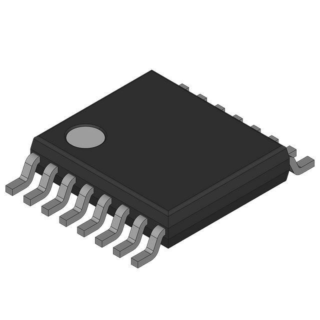
The DAC7573 is available in a 16-lead TSSOP
package.
IOVDD
VREFH
Data
Buffer A
DAC
Register A
VOUTA
DAC A
VOUTB
VOUTC
18
SCL
SDA
Data
Buffer D
DAC
Register D
Buffer
Control
Register
Control
I2C
Block
DAC D
Power-Down
Control Logic
Resistor
Network
8
A0
A1
GND
VOUTD
A2
A3 LDAC
VREFL
Please be aware that an important notice concerning availability, standard warranty, and use in critical applications of Texas
Instruments semiconductor products and disclaimers thereto appears at the end of this data sheet.
I2C is a trademark of Philips Corporation.
PRODUCTION DATA information is current as of publication date.
Products conform to specifications per the terms of the Texas
Instruments standard warranty. Production processing does not
necessarily include testing of all parameters.
Copyright © 2003, Texas Instruments Incorporated
�DAC7573
www.ti.com
SLAS398 – SEPTEMBER 2003
This integrated circuit can be damaged by ESD. Texas Instruments recommends that all integrated
circuits be handled with appropriate precautions. Failure to observe proper handling and installation
procedures can cause damage.
ESD damage can range from subtle performance degradation to complete device failure. Precision
integrated circuits may be more susceptible to damage because very small parametric changes could
cause the device not to meet its published specifications.
PACKAGE/ORDERING INFORMATION
PRODUCT
PACKAGE
PACKAGE
DRAWING
NUMBER
SPECIFICATION
TEMPERATURE
RANGE
PACKAGE
MARKING
DAC7573
16-TSSOP
PW
–40°C TO +105°C
D7573I
ORDERING
NUMBER
TRANSPORT MEDIA
DAC7573IPW
90 Piece Tube
DAC7573IPWR
2000 Piece Tape and Reel
PW PACKAGE
(TOPVIEW)
PIN DESCRIPTIONS
PIN
16 A3
NAME DESCRIPTION
1
VOUTA
Analog output voltage from DAC A
2
VOUTB
Analog output voltage from DAC B
Positive reference voltage input
VOUTA
1
VOUTB
2
15 A2
3
3
14 A1
VREFH
VREFH
4
VDD
VDD
4
13 A0
5
VREFL
Negative reference voltage input
VREFL
5
12 IOVDD
6
GND
GND
6
11 SDA
Ground reference point for all circuitry on the
part
VOUTC
7
10 SCL
VOUTD
8
9 LDAC
DAC7573
Analog voltage supply input
7
VOUTC Analog output voltage from DAC C
8
VOUTD Analog output voltage from DAC D
9
LDAC
10
SCL
H/W synchronous VOUT update
Serial clock input
11
SDA
Serial data input
12
IOVDD
13
A0
Device address select - I2C
14
A1
Device address select - I2C
15
A2
Device address select - Extended
16
A3
Device address select - Extended
I/O voltage supply input
ABSOLUTE MAXIMUM RATINGS (1)
VDD to GND
–0.3 V to +6 V
Digital input voltage to GND
–0.3 V to VDD + 0.3 V
VOUT to GND
–0.3 V to VDD + 0.3 V
Operating temperature range
–40°C to +105°C
Storage temperature range
–65°C to +150°C
Junction temperature range (TJ max)
Power dissipation:
Lead temperature, soldering:
(1)
2
+150°C
Thermal impedance (ΘJA)
161°C/W
Thermal impedance (ΘJC)
29°C/W
Vapor phase (60s)
215°C
Infrared (15s)
220°C
Stresses above those listed under Absolute Maximum Ratings may cause permanent damage to the device. Exposure to absolute
maximum conditions for extended periods may affect device reliability.
�DAC7573
www.ti.com
SLAS398 – SEPTEMBER 2003
ELECTRICAL CHARACTERISTICS
VDD = 2.7 V to 5.5 V, RL = 2 kΩ to GND; CL = 200 pF to GND; all specifications -40°C to +105°C, unless otherwise specified.
PARAMETER
TEST CONDITIONS
MIN
TYP
MAX
UNITS
STATIC PERFORMANCE (1) (2)
Resolution
12
Bits
Relative accuracy
Differential nonlinearity
Specified monotonic by design
±8
LSB
±1
LSB
Zero-scale error
5
20
mV
Full-scale error
-0.15
±1.0
% of FSR
±1.0
% of FSR
Gain error
Zero code error drift
±7
µV/°C
Gain temperature coefficient
±3
ppm of FSR/°C
OUTPUT CHARACTERISTICS (3)
Output voltage range
Output voltage settling time (full scale)
0
Digital-to-analog glitch impulse
12
µs
1
V/µs
0.02
LSB
1 kHz Sine Wave
-100
dB
RL= ∞
470
pF
RL= 2 kΩ
1000
pF
1 LSB change around major
carry
12
nV-s
0.3
nV-s
1
Ω
VDD= 5 V
50
mA
VDD= 3 V
20
mA
Coming out of power-down
mode, VDD= +5 V
2.5
µs
Coming out of power-down
mode, VDD= +3 V
5
µs
Digital feedthrough
DC output impedance
Short-circuit current
Power-up time
µs
RL = ∞ ; CL = 500 pF
DC crosstalk (channel-to-channel)
Capacitive load stability
V
10
8
Slew rate
AC crosstalk (channel-to-channel)
VREFH
RL = ∞; 0 pF < CL < 200 pF
REFERENCE INPUT
VREFH Input range
VREFL Input range
0
VREFL
很抱歉,暂时无法提供与“DAC7573IPWR”相匹配的价格&库存,您可以联系我们找货
免费人工找货