DAC5578
DAC6578
DAC7578
www.ti.com
SBAS496A – MARCH 2010 – REVISED AUGUST 2010
8-/10-/12-Bit, Octal-Channel, Ultra-Low Glitch, Voltage Output, Two-Wire Interface
Digital-to-Analog Converters
Check for Samples: DAC5578, DAC6578, DAC7578
FEATURES
DESCRIPTION
•
The DAC5578 (8 bit), DAC6578 (10 bit), and
DAC7578 (12 bit) are low-power, voltage-output, octal
channel, digital-to-analog converters (DACs). The
devices are monolithic, provide good linearity,and
minimize undesired code-to-code transient voltages
(glitch).
1
23
•
•
•
•
•
•
Relative Accuracy:
– DAC5578 (8 bit): 0.25LSB INL
– DAC6578 (10 bit): 0.5LSB INL
– DAC7578 (12 bit): 1LSB INL
Glitch Energy: 0.15nV-s
Power-On Reset to Zero Scale or Midscale
– Devices in the TSSOP Package Reset to
Zero Scale
– Devices in the QFN Package Reset to Zero
Scale or Midscale
Ultra-Low Power Operation: 0.13mA/ch at 5V
Wide Power-Supply Range: +2.7V to +5.5V
2-Wire Serial Interface ( I2C™ compatible)
Temperature Range: –40°C to +125°C
APPLICATIONS
•
•
•
•
Portable Instrumentation
Closed-Loop Servo Control
Process Control
Data Acquisition Systems
AVDD
Input Control Logic
VREFIN
Data Buffer H
DAC Register H
8-/10-/12-Bit
DAC
VOUTH
Data Buffer G
DAC Register G
8-/10-/12-Bit
DAC
VOUTG
DAC Register F
8-/10-/12-Bit
DAC
VOUTF
Data Buffer E
DAC Register E
8-/10-/12-Bit
DAC
VOUTE
Data Buffer D
DAC Register D
8-/10-/12-Bit
DAC
VOUTD
Data Buffer C
DAC Register C
8-/10-/12-Bit
DAC
VOUTC
Data Buffer B
DAC Register B
8-/10-/12-Bit
DAC
VOUTB
Data Buffer A
DAC Register A
8-/10-/12-Bit
DAC
VOUTA
Buffer Control
Register Control
LDAC
RSTSEL
8-BIT
10-BIT
12-BIT
Pin- and Function-Compatible
(w/internal reference)
—
—
DAC7678
Pin- and Function-Compatible
DAC5578
DAC6578
DAC7578
Power-Down
Control Logic
Control Logic
ADDR1
RELATED DEVICES
Data Buffer F
SDA
ADDR0
The devices incorporate a power-on-reset (POR)
circuit that ensures the DAC output powers up to
zero-scale or midscale until a valid code is written to
the device. These devices also contain a power-down
feature, accessed through the serial interface, that
reduces the current consumption of the devices to
typically 0.42mA at 5V. Power consumption is typically
2.32mW at 3V, reducing to 0.68mW in power-down
mode. The low power consumption and small
footprint make these devices ideal for portable,
battery-operated equipment.
The DAC5578, DAC6578, and DAC7578 are drop-in
and functionally-compatible with the DAC7678. All
devices are available in a 4x4, QFN-24 package and
a TSSOP-16 package.
DACx578
SCL
The devices use a versatile, 2-wire serial interface
that is I2C-compatible and operates at clock rates of
up to 3.4MHz. Multiple devices can share the same
bus.
CLR
GND
1
Please be aware that an important notice concerning availability, standard warranty, and use in critical applications of Texas
Instruments semiconductor products and disclaimers thereto appears at the end of this data sheet.
I C is a trademark of NXP Semiconductors.
All other trademarks are the property of their respective owners.
2
2
3
PRODUCTION DATA information is current as of publication date.
Products conform to specifications per the terms of the Texas
Instruments standard warranty. Production processing does not
necessarily include testing of all parameters.
Copyright © 2010, Texas Instruments Incorporated
�DAC5578
DAC6578
DAC7578
SBAS496A – MARCH 2010 – REVISED AUGUST 2010
www.ti.com
This integrated circuit can be damaged by ESD. Texas Instruments recommends that all integrated circuits be handled with
appropriate precautions. Failure to observe proper handling and installation procedures can cause damage.
ESD damage can range from subtle performance degradation to complete device failure. Precision integrated circuits may be more
susceptible to damage because very small parametric changes could cause the device not to meet its published specifications.
PACKAGE/ORDERING INFORMATION (1)
PRODUCT
MAXIMUM RELATIVE
ACCURACY
(LSB)
MAXIMUM
DIFFERENTIAL
NONLINEARITY
(LSB)
DAC7578
±1
±0.25
DAC6578
±0.5
DAC5578
(1)
±0.5
±0.25
±0.25
PACKAGELEAD
SPECIFIED
TEMPERATURE
RANGE
PACKAGE
DESIGNATOR
TSSOP-16
PW
QFN-24
RGE
TSSOP-16
PW
QFN-24
RGE
TSSOP-16
PW
QFN-24
RGE
–40°C to +125°C
–40°C to +125°C
–40°C to +125°C
PACKAGE
MARKING
DAC7578
DAC7578
DAC6578
DAC6578
DAC5578
DAC5578
For the most current package and ordering information see the Package Option Addendum at the end of this document, or see the TI
web site at www.ti.com.
ABSOLUTE MAXIMUM RATINGS (1)
Over operating free-air temperature range, unless otherwise noted.
DAC5578, DAC6578, DAC7578
UNIT
–0.3 to +6
V
Digital input voltage to GND
–0.3 to +AVDD + 0.3
V
VOUT to GND
–0.3 to +AVDD + 0.3
V
VREFIN to GND
–0.3 to +AVDD + 0.3
V
Operating temperature range
–40 to +125
°C
Storage temperature range
–65 to +150
°C
+150
°C
(TJ max – TA)/qJA
W
AVDD to GND
Junction temperature range (TJ max)
Power dissipation
(1)
Stresses above those listed under Absolute Maximum Ratings may cause permanent damage to the device. Exposure to absolute
maximum conditions for extended periods may affect device reliability.
THERMAL INFORMATION
THERMAL METRIC (1)
DACx578
PW (16 Pins)
RGE (24 PINS)
qJA
Junction-to-ambient thermal resistance
111.9
33.7
qJCtop
Junction-to-case (top) thermal resistance
33.3
16.9
qJB
Junction-to-board thermal resistance
52.4
7.4
yJT
Junction-to-top characterization parameter
2
0.5
yJB
Junction-to-board characterization parameter
51.2
7.1
qJCbot
Junction-to-case (bottom) thermal resistance
n/a
1.7
(1)
2
UNITS
°C/W
For more information about traditional and new thermal metrics, see the IC Package Thermal Metrics application report, SPRA953.
Submit Documentation Feedback
Copyright © 2010, Texas Instruments Incorporated
Product Folder Link(s): DAC5578 DAC6578 DAC7578
�DAC5578
DAC6578
DAC7578
www.ti.com
SBAS496A – MARCH 2010 – REVISED AUGUST 2010
ELECTRICAL CHARACTERISTICS
At AVDD = 2.7V to 5.5V and over –40°C to +125°C, unless otherwise noted.
PARAMETER
TEST CONDITIONS
DAC5578, DAC6578, DAC7578
MIN
UNIT
TYP
MAX
±0.01
±0.25
LSB
±0.01
±0.25
LSB
STATIC PERFORMANCE (1)
Resolution
DAC5578
Relative accuracy
8
Measured by the line passing through codes 4 and 250
Differential nonlinearity
Resolution
DAC6578
Relative accuracy
10
Measured by the line passing through codes 12 and
1012
Differential nonlinearity
Resolution
DAC7578
Relative accuracy
Measured by the line passing through codes 30 and
4050
Extrapolated from two-point line passing through two
codes (2), unloaded
Offset error drift
Full-scale error
±0.5
LSB
±0.03
±0.5
LSB
Bits
±0.3
±1
LSB
±0.1
±0.25
LSB
0.5
±4
mV
±0.03
mV/°C
±0.2
2
DAC register loaded with all '0's
1
Zero-code error drift
Gain error
±0.06
3
DAC register loaded with all '1's
Full-scale error drift
Zero-code error
Bits
12
Differential nonlinearity
Offset error
Bits
mV/°C
4
2
Extrapolated from two-point line passing through two
codes (2), unloaded
±0.01
Gain temperature coefficient
% of FSR
mV
mV/°C
±0.15
% of FSR
ppm of
FSR/°C
±1
OUTPUT CHARACTERISTICS (3)
Output voltage range
Output voltage settling time
0
DACs unloaded, 1/4 scale to 3/4 scale
RL = 1MΩ and CL = 470pF
Slew rate
Capacitive load stability
RL = ∞
AVDD
V
7
ms
12
ms
0.75
V/ms
470
pF
RL = 2kΩ
1000
pF
Code change glitch impulse
1LSB change around major carry
0.15
nV-s
Digital feedthrough
SCL toggling
1.5
nV-s
Power-on glitch
RL = ∞
Channel-to-channel dc crosstalk
3
mV
Full-scale swing on adjacent channel
0.1
LSB
DC output impedance
At midscale input
4.5
Ω
Short-circuit current
DAC outputs shorted to GND
25
mA
Power-up time (including settling time)
Coming out of power-down mode, AVDD = 5V
50
ms
(1)
(2)
(3)
Linearity calculated using a reduced code range; output unloaded.
12-bit: 30 and 4050; 10-bit: 12 and 1012; 8-bit: 4 and 250
Specified by design or characterization; not production tested.
Copyright © 2010, Texas Instruments Incorporated
Product Folder Link(s): DAC5578 DAC6578 DAC7578
Submit Documentation Feedback
3
�DAC5578
DAC6578
DAC7578
SBAS496A – MARCH 2010 – REVISED AUGUST 2010
www.ti.com
ELECTRICAL CHARACTERISTICS (continued)
At AVDD = 2.7V to 5.5V and over –40°C to +125°C, unless otherwise noted.
PARAMETER
TEST CONDITIONS
DAC5578, DAC6578, DAC7578
MIN
TYP
MAX
UNIT
AC PERFORMANCE (4)
DAC output noise density
TA = +25°C, at zero-code input, fOUT = 1kHz
DAC output noise
TA = +25°C, at midscale input, f = 0.1Hz to 10Hz
20
nV/√Hz
3
mVPP
60
µA
EXTERNAL REFERENCE
External reference current
AVDD = 2.7V to 5.5V
LOGIC INPUTS (4)
Input current
±1
mA
VINL
Logic input LOW voltage
2.7V ≤ AVDD ≤ 5.5V
GND-0.3
0.3xAVDD
V
VINH
Logic input HIGH voltage
2.7V ≤ AVDD ≤ 5.5V
0.7xAVDD
AVDD+0.3
V
3
pF
5.5
V
Pin capacitance
1.5
POWER REQUIREMENTS
AVDD
Analog power supply
Normal mode
IDD
(5)
All power-down modes
Normal mode
Power
dissipation (5)
All power-down modes
2.7
AVDD = 3.6V to 5.5V
VINH = AVDD and VINL = GND
1.02
1.4
mA
AVDD = 2.7V to 3.6V
VINH = AVDD and VINL = GND
0.86
1.3
mA
AVDD = 3.6V to 5.5V
VINH = AVDD and VINL = GND
0.42
6
mA
AVDD = 2.7V to 3.6V
VINH = AVDD and VINL = GND
0.25
4.7
mA
AVDD = 3.6V to 5.5V
VINH = AVDD and VINL = GND
3.67
7.7
mW
AVDD = 2.7V to 3.6V
VINH = AVDD and VINL = GND
2.32
4.68
mW
AVDD = 3.6V to 5.5V
VINH = AVDD and VINL = GND
1.51
33
mW
AVDD = 2.7V to 3.6V
VINH = AVDD and VINL = GND
0.68
16.92
mW
+125
°C
TEMPERATURE RANGE
Specified performance
(4)
(5)
4
–40
Specified by design or characterization; not production tested.
Input code = mid scale, no load.
Submit Documentation Feedback
Copyright © 2010, Texas Instruments Incorporated
Product Folder Link(s): DAC5578 DAC6578 DAC7578
�DAC5578
DAC6578
DAC7578
www.ti.com
SBAS496A – MARCH 2010 – REVISED AUGUST 2010
PIN CONFIGURATIONS
PW PACKAGE
TSSOP-16
(TOP VIEW)
TWOC
SDA
22
SCL
NC
23
21
20
19
LDAC
1
16
SCL
NC
LDAC
RGE PACKAGE
QFN-24
(TOP VIEW)
ADDR0
2
15
SDA
24
AVDD
3
14
GND
NC
1
18
VOUTA
4
13
VOUTB
AVDD
2
17
GND
VOUTA
3
16
VOUTB
VOUTC
4
15
VOUTD
VOUTE
5
14
VOUTF
VOUTG
6
13
VOUTH
VOUTE
6
11
VOUTF
VOUTG
7
10
VOUTH
VREFIN
8
9
CLR
DACx578
(Thermal pad)
NC
7
(1)
1
8
9
10
11
12
CLR
VOUTD
ADDR1
12
ADDR0
5
VREFIN
VOUTC
RSTSEL
DACx578
NC
It is recommended to connect the thermal
pad to GND for better thermal dissipation.
PIN DESCRIPTIONS
PACKAGE
NAME
DESCRIPTION
16-Pin
24-PIN
1
22
LDAC
2
11
ADDR0
3
2
AVDD
Power-supply input, 2.7V to 5.5V
4
3
VOUTA
Analog output voltage from DAC A
5
4
VOUTC
Analog output voltage from DAC C
6
5
VOUTE
Analog output voltage from DAC E
7
6
VOUTG
Analog output voltage from DAC G
8
8
VREFIN
Positive reference input
9
12
CLR
10
13
VOUTH
Analog output voltage from DAC H
11
14
VOUTF
Analog output voltage from DAC F
12
15
VOUTD
Analog output voltage from DAC D
13
16
VOUTB
Analog output voltage from DAC B
14
17
GND
Ground reference point for all circuitry on the device
15
19
SDA
Serial data input. Data are clocked into or out of the input register. This pin is a bidirectional,
open-drain data line that should be connected to the supply voltage with an external pull-up resistor.
16
20
SCL
Serial clock input. Data can be transferred at rates up to 3.4MHz. Schmitt-trigger logic input.
—
1
NC
Not internally connected
—
7
NC
Not internally connected
—
9
RSTSEL
Reset select pin. RSTSEL high resets device to mid-scale; RSTSEL low resets device to zero-scale.
—
10
ADDR1
3-state address input
—
18
NC
—
21
TWOC
—
23
NC
Not internally connected
—
24
NC
Not internally connected
Load DACs
3-state address input
Asynchronous clear input
Not internally connected
Twos complement select. If the TWOC pin is pulled high, the DAC registers use twos complement
format; if TWOC is pulled low, the DAC registers use straight binary format.
Copyright © 2010, Texas Instruments Incorporated
Product Folder Link(s): DAC5578 DAC6578 DAC7578
Submit Documentation Feedback
5
�DAC5578
DAC6578
DAC7578
SBAS496A – MARCH 2010 – REVISED AUGUST 2010
www.ti.com
TIMING DIAGRAM
tLOW
Low Byte Ack Cycle
tR
tHD:STA
tF
SCL
tHIGH
tHD:STA
tSU:STA
tSU:STO
tSU:DAT
tHD:DAT
SDA
tBUF
P
S
S
P
t1
LDAC1
t3
t2
LDAC2
t4
CLR
(1)
Asynchronous LDAC update mode. For more information and details, see the LDAC Functionality section.
(2)
Synchronous LDAC update mode. For more information and details, see the LDAC Functionality section.
Figure 1. Serial Write Operation
TIMING REQUIREMENTS (1)
At AVDD = 2.7 V to 5.5 V and –40°C to +125°C range (unless otherwise noted).
PARAMETER
STANDARD
MODE
FAST
MODE
MIN MAX
SCL frequency, fSCL
MIN
0.1
Bus free time between STOP and START conditions, tBUF
Hold time after repeated start, tHDSTA
HIGH SPEED
MODE
MAX
MIN
0.4
4.7
1.3
UNIT
MAX
3.4
MHz
µs
4
0.6
0.16
µs
4.7
0.6
0.16
µs
STOP condition setup time, tSUSTO
4
0.6
0.16
µs
Data hold time, tHDDAT
0
0
0
ns
Repeated Start setup time, tSUSTA
Data setup time, tSUDAT
250
100
10
ns
SCL clock LOW period, tLOW
4700
1300
160
ns
SCL clock HIGH period, tHIGH
4000
600
60
ns
Clock/Data fall time, tF
300
300
160
Clock/Data rise time, tR
1000
300
160
LDAC pulse width LOW time, t1
40
10
ns
ns
1.2
µs
SCL falling edge to LDAC falling edge for asynchronous LDAC update, t2
20
5
0.6
µs
LDAC falling edge to SCL falling edge for synchronous LDAC update, t3
360
90
10.5
µs
40
10
1.2
µs
CLR pulse width LOW time, t4
(1)
6
See the Serial Write Operation timing diagram.
Submit Documentation Feedback
Copyright © 2010, Texas Instruments Incorporated
Product Folder Link(s): DAC5578 DAC6578 DAC7578
�DAC5578
DAC6578
DAC7578
www.ti.com
SBAS496A – MARCH 2010 – REVISED AUGUST 2010
TYPICAL CHARACTERISTICS: DAC at AVDD = 5.5 V
At TA = 25°C, external reference used, DAC output not loaded, and all DAC codes in straight binary data format, DAC7578
graphs shown (unless otherwise noted).
LINEARITY ERROR
vs DIGITAL INPUT CODE (DAC7578, 12-Bit, –40°C)
DIFFERENTIAL LINEARITY ERROR
vs DIGITAL INPUT CODE (DAC7578, 12-Bit, –40°C)
1.0
0.25
All Eight Channels Shown
External Reference = 5V
0.8
0.15
0.4
DNL Error (LSB)
INL Error (LSB)
0.6
0.2
0.0
-0.2
-0.4
CH A
CH B
CH C
CH D
-0.6
-0.8
CH E
CH F
CH G
CH H
0.00
-0.05
-0.10
CH A
CH B
CH C
CH D
-0.20
CH E
CH F
CH G
CH H
-0.25
0
512
1024
1536 2048 2560
Digital Input Code
3072
3584
4096
0
512
1024
1536 2048 2560
Digital Input Code
3072
3584
4096
Figure 2.
Figure 3.
LINEARITY ERROR
vs DIGITAL INPUT CODE (DAC7578, 12-Bit, +25°C)
DIFFERENTIAL LINEARITY ERROR
vs DIGITAL INPUT CODE (DAC7578, 12-Bit, +25°C)
0.25
1.0
All Eight Channels Shown
External Reference = 5V
0.8
All Eight Channels Shown
External Reference = 5V
0.20
0.6
0.15
0.4
DNL Error (LSB)
INL Error (LSB)
0.10
0.05
-0.15
-1.0
0.2
0.0
-0.2
-0.4
CH A
CH B
CH C
CH D
-0.6
-0.8
CH E
CH F
CH G
CH H
0.10
0.05
0.00
-0.05
-0.10
CH A
CH B
CH C
CH D
-0.15
-0.20
-1.0
CH E
CH F
CH G
CH H
-0.25
0
512
1024
1536 2048 2560
Digital Input Code
3072
3584
4096
0
512
1024
1536 2048 2560
Digital Input Code
3072
3584
4096
Figure 4.
Figure 5.
LINEARITY ERROR
vs DIGITAL INPUT CODE (DAC7578, 12-Bit, +125°C)
DIFFERENTIAL LINEARITY ERROR
vs DIGITAL INPUT CODE (DAC7578, 12-Bit, +125°C)
1.0
0.25
All Eight Channels Shown
External Reference = 5V
0.8
All Eight Channels Shown
External Reference = 5V
0.20
0.6
0.15
0.4
DNL Error (LSB)
INL Error (LSB)
All Eight Channels Shown
External Reference = 5V
0.20
0.2
0.0
-0.2
-0.4
CH A
CH B
CH C
CH D
-0.6
-0.8
CH E
CH F
CH G
CH H
-1.0
0.10
0.05
0.00
-0.05
-0.10
CH A
CH B
CH C
CH D
-0.15
-0.20
CH E
CH F
CH G
CH H
-0.25
0
512
1024
1536 2048 2560
Digital Input Code
3072
3584
4096
0
512
1024
Figure 6.
1536 2048 2560
Digital Input Code
3072
3584
4096
Figure 7.
Copyright © 2010, Texas Instruments Incorporated
Product Folder Link(s): DAC5578 DAC6578 DAC7578
Submit Documentation Feedback
7
�DAC5578
DAC6578
DAC7578
SBAS496A – MARCH 2010 – REVISED AUGUST 2010
www.ti.com
TYPICAL CHARACTERISTICS: DAC at AVDD = 5.5 V (continued)
At TA = 25°C, external reference used, DAC output not loaded, and all DAC codes in straight binary data format, DAC7578
graphs shown (unless otherwise noted).
LINEARITY ERROR
vs DIGITAL INPUT CODE (DAC6578, 10-Bit, -40°C)
DIFFERENTIAL LINEARITY ERROR
vs DIGITAL INPUT CODE (DAC6578, 10-Bit, -40°C)
0.5
0.5
All Eight Channels Shown
External Reference = 5V
0.3
0.3
0.2
0.2
0.1
0.0
-0.1
-0.2
DAC A
DAC B
DAC C
DAC D
-0.3
-0.4
DAC E
DAC F
DAC G
DAC H
0.0
-0.1
-0.2
DAC A
DAC B
DAC C
DAC D
-0.4
128
256
384
512
640
Digital Input Code
768
896
1024
0
128
256
384
512
640
Digital Input Code
768
896
1024
Figure 8.
Figure 9.
LINEARITY ERROR
vs DIGITAL INPUT CODE (DAC6578, 10-Bit, +25°C)
DIFFERENTIAL LINEARITY ERROR
vs DIGITAL INPUT CODE (DAC6578, 10-Bit, +25°C)
0.5
0.5
All Eight Channels Shown
External Reference = 5V
0.4
0.2
0.2
DNL Error (LSB)
0.3
0.1
0.0
-0.1
DAC A
DAC B
DAC C
DAC D
-0.3
-0.4
All Eight Channels Shown
External Reference = 5V
0.4
0.3
-0.2
DAC E
DAC F
DAC G
DAC H
0.1
0.0
-0.1
-0.2
DAC A
DAC B
DAC C
DAC D
-0.3
-0.4
-0.5
DAC E
DAC F
DAC G
DAC H
-0.5
0
128
256
384
512
640
Digital Input Code
768
896
1024
0
128
256
384
512
640
Digital Input Code
768
896
1024
Figure 10.
Figure 11.
LINEARITY ERROR
vs DIGITAL INPUT CODE (DAC6578, 10-Bit, +125°C)
DIFFERENTIAL LINEARITY ERROR
vs DIGITAL INPUT CODE (DAC6578, 10-Bit, +125°C)
0.5
0.5
All Eight Channels Shown
External Reference = 5V
0.4
0.2
DNL Error (LSB)
0.3
0.2
0.1
0.0
-0.1
-0.2
DAC A
DAC B
DAC C
DAC D
-0.4
All Eight Channels Shown
External Reference = 5V
0.4
0.3
-0.3
DAC E
DAC F
DAC G
DAC H
-0.5
0.1
0.0
-0.1
-0.2
DAC A
DAC B
DAC C
DAC D
-0.3
-0.4
DAC E
DAC F
DAC G
DAC H
-0.5
0
128
256
384
512
640
Digital Input Code
768
896
1024
0
128
256
Figure 12.
8
DAC E
DAC F
DAC G
DAC H
-0.5
0
INL Error (LSB)
0.1
-0.3
-0.5
INL Error (LSB)
All Eight Channels Shown
External Reference = 5V
0.4
DNL Error (LSB)
INL Error (LSB)
0.4
Submit Documentation Feedback
384
512
640
Digital Input Code
768
896
1024
Figure 13.
Copyright © 2010, Texas Instruments Incorporated
Product Folder Link(s): DAC5578 DAC6578 DAC7578
�DAC5578
DAC6578
DAC7578
www.ti.com
SBAS496A – MARCH 2010 – REVISED AUGUST 2010
TYPICAL CHARACTERISTICS: DAC at AVDD = 5.5 V (continued)
At TA = 25°C, external reference used, DAC output not loaded, and all DAC codes in straight binary data format, DAC7578
graphs shown (unless otherwise noted).
LINEARITY ERROR
vs DIGITAL INPUT CODE (DAC5578, 8-Bit, -40°C)
DIFFERENTIAL LINEARITY ERROR
vs DIGITAL INPUT CODE (DAC5578, 8-Bit, -40°C)
0.25
0.25
All Eight Channels Shown
External Reference = 5V
0.15
0.15
0.10
0.10
0.05
0.00
-0.05
-0.10
DAC A
DAC B
DAC C
DAC D
-0.15
-0.20
DAC E
DAC F
DAC G
DAC H
0.00
-0.05
-0.10
DAC A
DAC B
DAC C
DAC D
-0.20
DAC E
DAC F
DAC G
DAC H
-0.25
0
32
64
96
128
160
Digital Input Code
192
224
256
0
32
64
96
128
160
Digital Input Code
192
224
256
Figure 14.
Figure 15.
LINEARITY ERROR
vs DIGITAL INPUT CODE (DAC5578, 8-Bit, +25°C)
DIFFERENTIAL LINEARITY ERROR
vs DIGITAL INPUT CODE (DAC5578, 8-Bit, +25°C)
0.25
0.25
All Eight Channels Shown
External Reference = 5V
0.20
All Eight Channels Shown
External Reference = 5V
0.20
0.15
0.15
0.10
DNL Error (LSB)
INL Error (LSB)
0.05
-0.15
-0.25
0.05
0.00
-0.05
-0.10
DAC A
DAC B
DAC C
DAC D
-0.15
-0.20
DAC E
DAC F
DAC G
DAC H
0.10
0.05
0.00
-0.05
-0.10
DAC A
DAC B
DAC C
DAC D
-0.15
-0.20
-0.25
DAC E
DAC F
DAC G
DAC H
-0.25
0
32
64
96
128
160
Digital Input Code
192
224
256
0
32
64
96
128
160
Digital Input Code
192
224
256
Figure 16.
Figure 17.
LINEARITY ERROR
vs DIGITAL INPUT CODE (DAC5578, 8-Bit, +125°C)
DIFFERENTIAL LINEARITY ERROR
vs DIGITAL INPUT CODE (DAC5578, 8-Bit, +125°C)
0.25
0.25
All Eight Channels Shown
External Reference = 5V
0.20
All Eight Channels Shown
External Reference = 5V
0.20
0.15
0.15
0.10
DNL Error (LSB)
INL Error (LSB)
All Eight Channels Shown
External Reference = 5V
0.20
DNL Error (LSB)
INL Error (LSB)
0.20
0.05
0.00
-0.05
-0.10
DAC A
DAC B
DAC C
DAC D
-0.15
-0.20
DAC E
DAC F
DAC G
DAC H
-0.25
0.10
0.05
0.00
-0.05
-0.10
DAC A
DAC B
DAC C
DAC D
-0.15
-0.20
DAC E
DAC F
DAC G
DAC H
-0.25
0
32
64
96
128
160
Digital Input Code
192
224
256
0
32
64
Figure 18.
96
128
160
Digital Input Code
192
224
256
Figure 19.
Copyright © 2010, Texas Instruments Incorporated
Product Folder Link(s): DAC5578 DAC6578 DAC7578
Submit Documentation Feedback
9
�DAC5578
DAC6578
DAC7578
SBAS496A – MARCH 2010 – REVISED AUGUST 2010
www.ti.com
TYPICAL CHARACTERISTICS: DAC at AVDD = 5.5 V (continued)
At TA = 25°C, external reference used, DAC output not loaded, and all DAC codes in straight binary data format, DAC7578
graphs shown (unless otherwise noted).
LINEARITY ERROR
vs TEMPERATURE (DAC7578, 12-Bit)
DIFFERENTIAL LINEARITY ERROR
vs TEMPERATURE (DAC7578, 12-Bit)
1.0
0.8
0.25
External Reference = 5V
0.15
0.4
INL MAX
DNL Error (LSB)
INL Error (LSB)
0.6
0.2
0.0
INL MIN
-0.2
-0.4
-0.6
DNL MAX
0.05
0.00
DNL MIN
-0.05
-0.10
-0.8
-0.20
-1.0
-40
-0.25
-40
0.4
-25
-10
5
20 35 50 65
Temperature (°C)
80
95
110 125
-25
-10
5
80
95
110 125
Figure 21.
LINEARITY ERROR
vs TEMPERATURE (DAC6578, 10-Bit)
DIFFERENTIAL LINEARITY ERROR
vs TEMPERATURE (DAC6578, 10-Bit)
0.5
External Reference = 5V
0.4
DNL Error (LSB)
0.2
INL MAX
0.1
0.0
-0.1
INL MIN
-0.3
0.2
0.1
DNL MAX
0.0
DNL MIN
-0.1
-0.2
-0.3
-0.4
-0.4
-0.5
-40
-0.5
-40
-25
-10
5
20 35 50 65
Temperature (°C)
80
95
110 125
-25
-10
5
20 35 50 65
Temperature (°C)
80
95
110 125
Figure 22.
Figure 23.
LINEARITY ERROR
vs TEMPERATURE (DAC5578, 8-Bit)
DIFFERENTIAL LINEARITY ERROR
vs TEMPERATURE (DAC5578, 8-Bit)
0.25
0.20
External Reference = 5V
0.3
-0.2
0.25
External Reference = 5V
0.20
0.15
External Reference = 5V
0.15
0.05
DNL Error (LSB)
0.10
INL MAX
0.00
INL MIN
-0.05
-0.10
-0.15
0.10
0.05
DNL MAX
0.00
DNL MIN
-0.05
-0.10
-0.15
-0.20
-0.20
-0.25
-40
-0.25
-40
-25
-10
5
20 35 50 65
Temperature (°C)
80
95
110 125
-25
-10
5
Figure 24.
10
20 35 50 65
Temperature (°C)
Figure 20.
0.3
INL Error (LSB)
0.10
-0.15
0.5
INL Error (LSB)
External Reference = 5V
0.20
Submit Documentation Feedback
20 35 50 65
Temperature (°C)
80
95
110 125
Figure 25.
Copyright © 2010, Texas Instruments Incorporated
Product Folder Link(s): DAC5578 DAC6578 DAC7578
�DAC5578
DAC6578
DAC7578
www.ti.com
SBAS496A – MARCH 2010 – REVISED AUGUST 2010
TYPICAL CHARACTERISTICS: DAC at AVDD = 5.5 V (continued)
At TA = 25°C, external reference used, DAC output not loaded, and all DAC codes in straight binary data format, DAC7578
graphs shown (unless otherwise noted).
POWER SUPPLY CURRENT
vs TEMPERATURE
OFFSET ERROR
vs TEMPERATURE
4
1.4
3
1.3
1.2
1.1
1.0
1
0
-1
-2
0.9
-25
-10
5
20 35 50 65
Temperature (°C)
80
95
-4
-40
110 125
-25
-10
5
20 35 50 65
Temperature (°C)
80
Figure 26.
Figure 27.
POWER-DOWN CURRENT
vs TEMPERATURE
FULL-SCALE ERROR
vs TEMPERATURE
CH E
CH F
CH G
CH H
95
110 125
0.20
6
External Reference = 5V
External Reference = 5V
0.15
Full-Scale Error (%FSR)
5
4
3
2
1
0
-40
CH A
CH B
CH C
CH D
-3
0.8
-40
Power Supply Current (μA)
External Reference = 5V
2
Offset Error (mV)
Power Supply Current (mA)
External Reference = 5V
0.10
0.05
0.00
-0.05
-0.10
DAC A
DAC B
DAC C
DAC D
-0.15
-25
-10
5
20 35 50 65
Temperature (°C)
80
95
-0.20
-40
110 125
-25
-10
5
20 35 50 65
Temperature (°C)
Figure 28.
80
DAC E
DAC F
DAC G
DAC H
95
110 125
Figure 29.
GAIN ERROR
vs TEMPERATURE
0.15
External Reference = 5V
Gain Error (%FSR)
0.10
0.05
0.00
-0.05
DAC A
DAC B
DAC C
DAC D
-0.10
-0.15
-40
-25
-10
5
20 35 50 65
Temperature (°C)
80
DAC E
DAC F
DAC G
DAC H
95
110 125
Figure 30.
Copyright © 2010, Texas Instruments Incorporated
Product Folder Link(s): DAC5578 DAC6578 DAC7578
Submit Documentation Feedback
11
�DAC5578
DAC6578
DAC7578
SBAS496A – MARCH 2010 – REVISED AUGUST 2010
www.ti.com
TYPICAL CHARACTERISTICS: DAC at AVDD = 5.5 V (continued)
At TA = 25°C, external reference used, DAC output not loaded, and all DAC codes in straight binary data format, DAC7578
graphs shown (unless otherwise noted).
SOURCE CURRENT
AT POSITIVE RAIL
SINK CURRENT
AT NEGATIVE RAIL
0.6
5.00
Channel C
DAC Loaded With 000h
0.5
Output Voltage (V)
Output Voltage (V)
4.95
4.90
0.4
0.3
0.2
4.85
0.1
Channel C
DAC Loaded With FFFh
4.80
0.0
0
1
2
3
4
5
6
7
Source Current (mA)
8
9
10
0
1
2
3
4
5
6
Sink Current (mA)
7
Figure 31.
Figure 32.
SOURCE CURRENT
AT POSITIVE RAIL
SINK CURRENT
AT NEGATIVE RAIL
8
9
10
8
9
10
8
9
10
0.6
5.00
Channel D
DAC Loaded With 000h
0.5
Output Voltage (V)
Output Voltage (V)
4.95
4.90
0.4
0.3
0.2
4.85
0.1
Channel D
DAC Loaded With FFFh
4.80
0.0
0
1
2
3
4
5
6
7
Source Current (mA)
8
9
10
0
1
2
3
4
5
6
Sink Current (mA)
7
Figure 33.
Figure 34.
SOURCE CURRENT
AT POSITIVE RAIL
SINK CURRENT
AT NEGATIVE RAIL
0.6
5.00
Channel H
DAC Loaded With 000h
0.5
Output Voltage (V)
Output Voltage (V)
4.95
4.90
0.4
0.3
0.2
4.85
0.1
Channel H
DAC Loaded With FFFh
4.80
0.0
0
1
2
3
4
5
6
7
Source Current (mA)
8
9
10
0
1
2
3
Figure 35.
12
Submit Documentation Feedback
4
5
6
Sink Current (mA)
7
Figure 36.
Copyright © 2010, Texas Instruments Incorporated
Product Folder Link(s): DAC5578 DAC6578 DAC7578
�DAC5578
DAC6578
DAC7578
www.ti.com
SBAS496A – MARCH 2010 – REVISED AUGUST 2010
TYPICAL CHARACTERISTICS: DAC at AVDD = 5.5 V (continued)
At TA = 25°C, external reference used, DAC output not loaded, and all DAC codes in straight binary data format, DAC7578
graphs shown (unless otherwise noted).
POWER SUPPLY CURRENT
vs POWER SUPPLY VOLTAGE
1.4
1.4
1.2
1.3
Power Supply Current (mA)
1.0
0.8
0.6
0.4
0.2
External Reference = 5V
Code Loaded to all Eight DAC Channels
512
1024
1536 2048 2560
Digital Input Code
3072
3584
1.0
0.9
0.8
3.1
3.5
3.9
4.3
4.7
Power Supply Voltage (V)
Figure 37.
Figure 38.
POWER DOWN CURRENT
vs POWER SUPPLY VOLTAGE
POWER-SUPPLY CURRENT
HISTOGRAM
5.1
5.5
14
AVDD = 2.7V to 5.5V
External Reference = 5V
12
0.35
10
0.30
% of Population
Power Supply Current (mA)
1.1
0.6
2.7
4096
0.45
0.40
1.2
0.7
0.0
0
AVDD = 2.7V to 5.5V
0.25
0.20
0.15
8
6
4
0.10
2
0.05
0.00
2.7
0
3.1
3.5
3.9
4.3
4.7
Power Supply Voltage (V)
5.1
5.5
0.90
0.91
0.92
0.93
0.94
0.95
0.96
0.97
0.98
0.99
1.00
1.01
1.02
1.03
1.04
1.05
1.06
1.07
1.08
1.09
1.10
1.11
1.12
1.13
1.14
1.15
Power Supply Current (mA)
POWER SUPPLY CURRENT
vs DIGITAL INPUT CODE
Supply Current (mA)
Figure 39.
Figure 40.
FULL-SCALE SETTLING TIME:
5V RISING EDGE
FULL-SCALE SETTLING TIME:
5V FALLING EDGE
From Code FFFh to 000h
Zoomed Rising Edge
100 mV/div
Zoomed Falling Edge
100 mV/div
Falling Edge
2 V/div
Rising Edge
2 V/div
Trigger Pulse
5 V/div
From Code 000h to FFFh
Trigger Pulse
5 V/div
Time (5 ms/div)
Time (5 ms/div)
Figure 41.
Figure 42.
Copyright © 2010, Texas Instruments Incorporated
Product Folder Link(s): DAC5578 DAC6578 DAC7578
Submit Documentation Feedback
13
�DAC5578
DAC6578
DAC7578
SBAS496A – MARCH 2010 – REVISED AUGUST 2010
www.ti.com
TYPICAL CHARACTERISTICS: DAC at AVDD = 5.5 V (continued)
At TA = 25°C, external reference used, DAC output not loaded, and all DAC codes in straight binary data format, DAC7578
graphs shown (unless otherwise noted).
HALF-SCALE SETTLING TIME:
5V RISING EDGE
HALF-SCALE SETTLING TIME:
5V FALLING EDGE
From Code 400h to C00h
Zoomed Rising Edge
100 mV/div
From Code C00h to 400h
Zoomed Falling Edge
100 mV/div
Falling Edge
2 V/div
Rising Edge
2 V/div
Trigger Pulse
5 V/div
Trigger Pulse
5 V/div
Time (5 ms/div)
Time (5 ms/div)
Figure 43.
Figure 44.
CLOCK FEEDTHROUGH
400 kHz MIDSCALE
POWER-ON GLITCH
RESET TO ZERO SCALE
AVDD = 5.5 V,
Clock Feedthrough Impulse ~1.5 nV-s
DAC Unloaded
DAC at Zero Scale
VOUT - 2 mV/div
~2 mVPP
VOUT - 5 mV/div
AVDD - 2 V/div
SCL - 5 V/div
Time (10 ms/div)
t - Time - 1 ms/div
Figure 45.
Figure 46.
POWER-ON GLITCH
RESET-TO-MID SCALE
POWER-OFF GLITCH
DAC Unloaded
DAC at Zero Scale
DAC Unloaded
DAC at Zero Scale
VOUT - 2 V/div
VOUT - 1 mV/div
AVDD - 2 V/div
AVDD - 2 V/div
Time (20 ms/div)
Time (10 ms/div)
Figure 47.
14
G045
Submit Documentation Feedback
Figure 48.
Copyright © 2010, Texas Instruments Incorporated
Product Folder Link(s): DAC5578 DAC6578 DAC7578
�DAC5578
DAC6578
DAC7578
www.ti.com
SBAS496A – MARCH 2010 – REVISED AUGUST 2010
TYPICAL CHARACTERISTICS: DAC at AVDD = 5.5 V (continued)
At TA = 25°C, external reference used, DAC output not loaded, and all DAC codes in straight binary data format, DAC7578
graphs shown (unless otherwise noted).
GLITCH ENERGY:
5V, 12-BIT, 1LSB STEP, RISING EDGE
GLITCH ENERGY:
5V, 12-BIT, 1LSB STEP, FALLING EDGE
From Code 801h to 800h
From Code 800h to 801h
VOUT - 500 mV/div
LDAC Clock
Feed-Through
VOUT - 500 mV/div
LDAC Clock
Feed-Through
LDAC - Trigger Pulse
5 V/div
LDAC - Trigger Pulse
5 V/div
Time (2 ms/div)
Time (2 ms/div)
Figure 49.
Figure 50.
GLITCH ENERGY:
5V, 10-BIT, 1LSB STEP, RISING EDGE
GLITCH ENERGY:
5V, 10-BIT, 1LSB STEP, FALLING EDGE
From Code 200h to 201h
From Code 201h to 200h
VOUT - 2 mV/div
VOUT - 2 mV/div
LDAC Clock
Feed-Through
LDAC Clock
Feed-Through
LDAC - Trigger Pulse
5 V/div
LDAC - Trigger Pulse
5 V/div
Time (2 ms/div)
Time (2 ms/div)
Figure 51.
Figure 52.
GLITCH ENERGY:
5V, 8-BIT, 1LSB STEP, RISING EDGE
GLITCH ENERGY:
5V, 8-BIT, 1LSB STEP, FALLING EDGE
From Code 80h to 81h
From Code 81h to 801h
VOUT - 5 mV/div
VOUT - 5 mV/div
LDAC Clock
Feed-Through
LDAC Clock
Feed-Through
LDAC - Trigger Pulse
5 V/div
LDAC - Trigger Pulse
5 V/div
Time (2 ms/div)
Time (2 ms/div)
Figure 53.
Figure 54.
Copyright © 2010, Texas Instruments Incorporated
Product Folder Link(s): DAC5578 DAC6578 DAC7578
Submit Documentation Feedback
15
�DAC5578
DAC6578
DAC7578
SBAS496A – MARCH 2010 – REVISED AUGUST 2010
www.ti.com
TYPICAL CHARACTERISTICS: DAC at AVDD = 5.5 V (continued)
At TA = 25°C, external reference used, DAC output not loaded, and all DAC codes in straight binary data format, DAC7578
graphs shown (unless otherwise noted).
DAC OUTPUT NOISE
0.1 Hz to 10 Hz
DAC OUTPUT NOISE DENSITY
vs FREQUENCY
300
DAC Output Unloaded
External Reference = 5V
200
150
VOUT (1 mV/div)
Voltage Noise (nV/√Hz)
250
Full Scale
100
Mid Scale
~3 mVPP
50
Zero Scale
0
20
100
1k
Frequency (Hz)
10k
100k
Time (2 s/div)
Figure 55.
16
Submit Documentation Feedback
Figure 56.
Copyright © 2010, Texas Instruments Incorporated
Product Folder Link(s): DAC5578 DAC6578 DAC7578
�DAC5578
DAC6578
DAC7578
www.ti.com
SBAS496A – MARCH 2010 – REVISED AUGUST 2010
TYPICAL CHARACTERISTICS: DAC AT AVDD = 3.6 V
At TA = 25°C, external reference used, DAC output not loaded, and all DAC codes in straight binary data format, DAC7578
graphs shown (unless otherwise noted).
POWER SUPPLY CURRENT
vs TEMPERATURE
POWER SUPPLY CURRENT
vs DIGITAL INPUT CODE
1.3
1.30
1.20
1.2
1.10
Power Supply Current - mA
Power Supply Current (mA)
External Reference = 3.3V
1.1
1.0
0.9
0.8
1.00
0.90
0.80
0.70
0.60
0.50
0.40
AVDD = 3.6 V,
External Reference = 3.3 V,
Code Loaded to all Eight DAC Channels
0.30
0.20
0.7
-40
0.10
-25
-10
5
20 35 50 65
Temperature (°C)
80
95
110 125
0.00
0
512
1024
Figure 57.
1536
2048
2560
Digital Input Code
3072
3584
4096
Figure 58.
POWER SUPPLY CURRENT HISTOGRAM
14
AVDD = 3.6 V,
External Reference = 3.3 V
12
% of Population
10
8
6
4
0
0.765
0.775
0.785
0.795
0.805
0.815
0.825
0.835
0.845
0.855
0.865
0.875
0.885
0.895
0.905
0.915
0.925
0.935
0.945
0.955
0.965
0.975
2
IDD - Supply Current - mA
Figure 59.
Copyright © 2010, Texas Instruments Incorporated
Product Folder Link(s): DAC5578 DAC6578 DAC7578
Submit Documentation Feedback
17
�DAC5578
DAC6578
DAC7578
SBAS496A – MARCH 2010 – REVISED AUGUST 2010
www.ti.com
TYPICAL CHARACTERISTICS: DAC AT AVDD = 2.7 V
At TA = 25°C, external reference used, DAC output not loaded, and all DAC codes in straight binary data format, DAC7578
graphs shown (unless otherwise noted).
LINEARITY ERROR
vs DIGITAL INPUT CODE (DAC7578, 12-Bit, –40°C)
DIFFERENTIAL LINEARITY ERROR
vs DIGITAL INPUT CODE (DAC7578, 12-Bit, –40°C)
0.25
1.0
All Eight Channels Shown
External Reference = 2.5V
0.8
0.15
0.4
DNL Error (LSB)
INL Error (LSB)
0.6
0.2
0.0
-0.2
-0.4
CH A
CH B
CH C
CH D
-0.6
-0.8
CH E
CH F
CH G
CH H
0.00
-0.05
-0.10
CH A
CH B
CH C
CH D
-0.20
512
1024
1536 2048 2560
Digital Input Code
3072
3584
4096
0
512
1024
1536 2048 2560
Digital Input Code
3072
3584
4096
Figure 60.
Figure 61.
LINEARITY ERROR
vs DIGITAL INPUT CODE (DAC7578, 12-Bit, +25°C)
DIFFERENTIAL LINEARITY ERROR
vs DIGITAL INPUT CODE (DAC7578, 12-Bit, +25°C)
1.0
0.25
0.8
0.20
0.6
0.15
DNL Error (LSB)
0.4
0.2
0.0
-0.2
-0.4
CH A
CH B
CH C
CH D
-0.6
-0.8
CH E
CH F
CH G
CH H
0.10
0.05
0.00
-0.05
-0.10
CH A
CH B
CH C
CH D
-0.15
-0.20
-1.0
CH E
CH F
CH G
CH H
-0.25
0
512
1024
1536 2048 2560
Digital Input Code
3072
3584
4096
0
512
1024
1536 2048 2560
Digital Input Code
3072
3584
4096
Figure 62.
Figure 63.
LINEARITY ERROR
vs DIGITAL INPUT CODE (DAC7578, 12-Bit, +125°C)
DIFFERENTIAL LINEARITY ERROR
vs DIGITAL INPUT CODE (DAC7578, 12-Bit, +125°C)
1.0
0.8
0.25
All Eight Channels Shown
External Reference = 2.5V
0.15
DNL Error (LSB)
0.4
0.2
0.0
-0.2
-0.4
CH A
CH B
CH C
CH D
-0.6
-0.8
-1.0
0
All Eight Channels Shown
External Reference = 2.5V
0.20
0.6
CH E
CH F
CH G
CH H
0.10
0.05
0.00
-0.05
-0.10
CH A
CH B
CH C
CH D
-0.15
-0.20
CH E
CH F
CH G
CH H
-0.25
512
1024
1536 2048 2560
Digital Input Code
3072
3584
4096
0
512
1024
Figure 64.
18
CH E
CH F
CH G
CH H
-0.25
0
INL Error (LSB)
0.10
0.05
-0.15
-1.0
INL Error (LSB)
All Eight Channels Shown
External Reference = 2.5V
0.20
Submit Documentation Feedback
1536 2048 2560
Digital Input Code
3072
3584
4096
Figure 65.
Copyright © 2010, Texas Instruments Incorporated
Product Folder Link(s): DAC5578 DAC6578 DAC7578
�DAC5578
DAC6578
DAC7578
www.ti.com
SBAS496A – MARCH 2010 – REVISED AUGUST 2010
TYPICAL CHARACTERISTICS: DAC AT AVDD = 2.7 V (continued)
At TA = 25°C, external reference used, DAC output not loaded, and all DAC codes in straight binary data format, DAC7578
graphs shown (unless otherwise noted).
LINEARITY ERROR
vs DIGITAL INPUT CODE (DAC6578, 10-Bit, –40°C)
DIFFERENTIAL LINEARITY ERROR
vs DIGITAL INPUT CODE (DAC6578, 10-Bit, –40°C)
0.5
0.5
All Eight Channels Shown
External Reference = 2.5V
0.3
0.3
0.2
0.2
0.1
0.0
-0.1
-0.2
DAC A
DAC B
DAC C
DAC D
-0.3
-0.4
DAC E
DAC F
DAC G
DAC H
-0.1
-0.2
DAC A
DAC B
DAC C
DAC D
-0.4
DAC E
DAC F
DAC G
DAC H
-0.5
0
128
256
384
512
640
Digital Input Code
768
896
1024
0
128
256
384
512
640
Digital Input Code
768
896
1024
Figure 66.
Figure 67.
LINEARITY ERROR
vs DIGITAL INPUT CODE (DAC6578, 10-Bit, +25°C)
DIFFERENTIAL LINEARITY ERROR
vs DIGITAL INPUT CODE (DAC6578, 10-Bit, +25°C)
0.5
0.5
All Eight Channels Shown
External Reference = 2.5V
0.4
All Eight Channels Shown
External Reference = 2.5V
0.4
0.3
0.3
0.2
0.2
DNL Error (LSB)
INL Error (LSB)
0.1
0.0
-0.3
-0.5
0.1
0.0
-0.1
-0.2
DAC A
DAC B
DAC C
DAC D
-0.3
-0.4
DAC E
DAC F
DAC G
DAC H
0.1
0.0
-0.1
-0.2
DAC A
DAC B
DAC C
DAC D
-0.3
-0.4
-0.5
DAC E
DAC F
DAC G
DAC H
-0.5
0
128
256
384
512
640
Digital Input Code
768
896
1024
0
128
256
384
512
640
Digital Input Code
768
896
1024
Figure 68.
Figure 69.
LINEARITY ERROR
vs DIGITAL INPUT CODE (DAC6578, 10-Bit, +125°C)
DIFFERENTIAL LINEARITY ERROR
vs DIGITAL INPUT CODE (DAC6578, 10-Bit, +125°C)
0.5
0.5
All Eight Channels Shown
External Reference = 2.5V
0.4
All Eight Channels Shown
External Reference = 2.5V
0.4
0.3
0.3
0.2
0.2
DNL Error (LSB)
INL Error (LSB)
All Eight Channels Shown
External Reference = 2.5V
0.4
DNL Error (LSB)
INL Error (LSB)
0.4
0.1
0.0
-0.1
-0.2
DAC A
DAC B
DAC C
DAC D
-0.3
-0.4
DAC E
DAC F
DAC G
DAC H
-0.5
0.1
0.0
-0.1
-0.2
DAC A
DAC B
DAC C
DAC D
-0.3
-0.4
DAC E
DAC F
DAC G
DAC H
-0.5
0
128
256
384
512
640
Digital Input Code
768
896
1024
0
128
256
Figure 70.
384
512
640
Digital Input Code
768
896
1024
Figure 71.
Copyright © 2010, Texas Instruments Incorporated
Product Folder Link(s): DAC5578 DAC6578 DAC7578
Submit Documentation Feedback
19
�DAC5578
DAC6578
DAC7578
SBAS496A – MARCH 2010 – REVISED AUGUST 2010
www.ti.com
TYPICAL CHARACTERISTICS: DAC AT AVDD = 2.7 V (continued)
At TA = 25°C, external reference used, DAC output not loaded, and all DAC codes in straight binary data format, DAC7578
graphs shown (unless otherwise noted).
LINEARITY ERROR
vs DIGITAL INPUT CODE (DAC5578, 8-Bit, –40°C)
DIFFERENTIAL LINEARITY ERROR
vs DIGITAL INPUT CODE (DAC5578, 8-Bit, –40°C)
0.25
0.25
All Eight Channels Shown
External Reference = 2.5V
0.15
0.15
0.10
0.10
0.05
0.00
-0.05
-0.10
DAC A
DAC B
DAC C
DAC D
-0.15
-0.20
DAC E
DAC F
DAC G
DAC H
0.00
-0.05
-0.10
DAC A
DAC B
DAC C
DAC D
-0.20
32
64
96
128
160
Digital Input Code
192
224
256
0
32
64
96
128
160
Digital Input Code
192
224
256
Figure 72.
Figure 73.
LINEARITY ERROR
vs DIGITAL INPUT CODE (DAC5578, 8-Bit, +25°C)
DIFFERENTIAL LINEARITY ERROR
vs DIGITAL INPUT CODE (DAC5578, 8-Bit, +25°C)
0.25
0.25
All Eight Channels Shown
External Reference = 2.5V
0.20
All Eight Channels Shown
External Reference = 2.5V
0.20
0.15
0.15
DNL Error (LSB)
0.10
0.05
0.00
-0.05
-0.10
DAC A
DAC B
DAC C
DAC D
-0.15
-0.20
DAC E
DAC F
DAC G
DAC H
0.10
0.05
0.00
-0.05
-0.10
DAC A
DAC B
DAC C
DAC D
-0.15
-0.20
-0.25
DAC E
DAC F
DAC G
DAC H
-0.25
0
32
64
96
128
160
Digital Input Code
192
224
256
0
32
64
96
128
160
Digital Input Code
192
224
256
Figure 74.
Figure 75.
LINEARITY ERROR
vs DIGITAL INPUT CODE (DAC5578, 8-Bit, +125°C)
DIFFERENTIAL LINEARITY ERROR
vs DIGITAL INPUT CODE (DAC5578, 8-Bit, +125°C)
0.25
0.25
All Eight Channels Shown
External Reference = 2.5V
0.20
All Eight Channels Shown
External Reference = 2.5V
0.20
0.15
0.15
DNL Error (LSB)
0.10
0.05
0.00
-0.05
-0.10
DAC A
DAC B
DAC C
DAC D
-0.15
-0.20
DAC E
DAC F
DAC G
DAC H
-0.25
0.10
0.05
0.00
-0.05
-0.10
DAC A
DAC B
DAC C
DAC D
-0.15
-0.20
DAC E
DAC F
DAC G
DAC H
-0.25
0
32
64
96
128
160
Digital Input Code
192
224
256
0
32
64
Figure 76.
20
DAC E
DAC F
DAC G
DAC H
-0.25
0
INL Error (LSB)
0.05
-0.15
-0.25
INL Error (LSB)
All Eight Channels Shown
External Reference = 2.5V
0.20
DNL Error (LSB)
INL Error (LSB)
0.20
Submit Documentation Feedback
96
128
160
Digital Input Code
192
224
256
Figure 77.
Copyright © 2010, Texas Instruments Incorporated
Product Folder Link(s): DAC5578 DAC6578 DAC7578
�DAC5578
DAC6578
DAC7578
www.ti.com
SBAS496A – MARCH 2010 – REVISED AUGUST 2010
TYPICAL CHARACTERISTICS: DAC AT AVDD = 2.7 V (continued)
At TA = 25°C, external reference used, DAC output not loaded, and all DAC codes in straight binary data format, DAC7578
graphs shown (unless otherwise noted).
DIFFERENTIAL LINEARITY ERROR
vs TEMPERATURE (DAC7578, 12-BIT)
1.00
0.25
0.80 External Reference = 2.5V
0.20
0.60
0.15
INL MAX
0.40
DNL Error (LSB)
INL Error (LSB)
LINEARITY ERROR
vs TEMPERATURE (DAC7578, 12-BIT)
0.20
0.00
INL MIN
-0.20
-0.40
External Reference = 2.5V
DNL MAX
0.10
0.05
0.00
DNL MIN
-0.05
-0.10
-0.15
-0.60
-0.20
-0.80
-1.00
-40
-25
-10
5
20
35
50
65
80
95
110
-0.25
-40
125
-25
-10
5
20 35 50 65
Temperature (°C)
80
95
110 125
Temperature (°C)
Figure 78.
Figure 79.
LINEARITY ERROR
vs TEMPERATURE (DAC6578, 10-Bit)
DIFFERENTIAL LINEARITY ERROR
vs TEMPERATURE (DAC6578, 10-Bit)
0.5
0.4
0.5
External Reference = 2.5V
0.4
0.3
0.2
DNL Error (LSB)
INL Error (LSB)
0.3
INL MAX
0.1
0.0
-0.1
INL MIN
-0.2
0.1
-0.1
-0.4
-10
5
20 35 50 65
Temperature (°C)
80
95
-0.5
-40
110 125
0.20
DNL MIN
-0.2
-0.3
-25
DNL MAX
0.0
-0.4
-25
-10
5
20 35 50 65
Temperature (°C)
80
95
110 125
Figure 80.
Figure 81.
LINEARITY ERROR
vs TEMPERATURE (DAC5578, 8-Bit)
DIFFERENTIAL LINEARITY ERROR
vs TEMPERATURE (DAC5578, 8-Bit)
0.25
0.25
External Reference = 2.5V
0.20
0.15
0.15
0.10
0.10
0.05
DNL Error (LSB)
INL Error (LSB)
0.2
-0.3
-0.5
-40
External Reference = 2.5V
INL MAX
0.00
INL MIN
-0.05
-0.10
-0.15
External Reference = 2.5V
0.05
DNL MAX
0.00
DNL MIN
-0.05
-0.10
-0.15
-0.20
-0.20
-0.25
-40
-0.25
-40
-25
-10
5
20 35 50 65
Temperature (°C)
80
95
110 125
-25
-10
5
Figure 82.
20 35 50 65
Temperature (°C)
80
95
110 125
Figure 83.
Copyright © 2010, Texas Instruments Incorporated
Product Folder Link(s): DAC5578 DAC6578 DAC7578
Submit Documentation Feedback
21
�DAC5578
DAC6578
DAC7578
SBAS496A – MARCH 2010 – REVISED AUGUST 2010
www.ti.com
TYPICAL CHARACTERISTICS: DAC AT AVDD = 2.7 V (continued)
At TA = 25°C, external reference used, DAC output not loaded, and all DAC codes in straight binary data format, DAC7578
graphs shown (unless otherwise noted).
POWER-SUPPLY CURRENT
vs TEMPERATURE
OFFSET ERROR
vs TEMPERATURE
4
1.3
External Reference = 2.5V
3
1.0
0.9
0.8
0
-1
DAC A
DAC B
DAC C
DAC D
-3
-25
-10
5
20 35 50 65
Temperature (°C)
80
95
-4
-40
110 125
-25
-10
5
20 35 50 65
Temperature (°C)
80
Figure 84.
Figure 85.
POWER-DOWN CURRENT
vs TEMPERATURE
FULL-SCALE ERROR
vs TEMPERATURE
DAC E
DAC F
DAC G
DAC H
95
110 125
0.20
4.70
4.50
AVDD = 2.7 V,
4.20
External Reference = 2.5 V
3.90
3.60
External Reference = 2.5V
0.15
Full-Scale Error (%FSR)
Power Supply Current - mA
1
-2
0.7
0.6
-40
External Reference = 2.5V
2
1.1
Offset Error (mV)
Power Supply Current (mA)
1.2
3.30
3.00
2.70
2.40
2.10
1.80
1.50
0.10
0.05
0.00
-0.05
-0.10
DAC A
DAC B
DAC C
DAC D
1.20
0.90
-0.15
0.60
0.30
0.00
-40
-0.20
-40
-25
-10
5
20
35
50
65
T - Temperature -°C
80
95
110
-25
-10
5
125
Figure 86.
20 35 50 65
Temperature (°C)
80
DAC E
DAC F
DAC G
DAC H
95
110 125
Figure 87.
GAIN ERROR
vs TEMPERATURE
0.15
External Reference = 2.5V
Gain Error (%FSR)
0.10
0.05
0.0
-0.05
DAC A
DAC B
DAC C
DAC D
-0.10
-0.15
-40
-25
-10
5
20 35 50 65
Temperature (°C)
80
DAC E
DAC F
DAC G
DAC H
95
110 125
Figure 88.
22
Submit Documentation Feedback
Copyright © 2010, Texas Instruments Incorporated
Product Folder Link(s): DAC5578 DAC6578 DAC7578
�DAC5578
DAC6578
DAC7578
www.ti.com
SBAS496A – MARCH 2010 – REVISED AUGUST 2010
TYPICAL CHARACTERISTICS: DAC AT AVDD = 2.7 V (continued)
At TA = 25°C, external reference used, DAC output not loaded, and all DAC codes in straight binary data format, DAC7578
graphs shown (unless otherwise noted).
SOURCE CURRENT
AT POSITIVE RAIL
SINK CURRENT
AT NEGATIVE RAIL
0.6
2.500
Channel A
DAC Loaded With FFFh
External Reference = 2.5V
2.495
2.485
Output Voltage (V)
Output Voltage (V)
2.490
Channel A
DAC Loaded With 000h
External Reference = 2.5V
0.5
2.480
2.475
2.470
2.465
2.460
0.4
0.3
0.2
0.1
2.455
2.450
0.0
0
1
2
3
4
5
6
7
Source Current (mA)
8
9
10
0
2
3
4
5
6
Sink Current (mA)
7
Figure 89.
Figure 90.
SOURCE CURRENT
AT POSITIVE RAIL
SINK CURRENT
AT NEGATIVE RAIL
8
9
10
8
9
10
8
9
10
0.6
2.500
Channel B
DAC Loaded With FFFh
External Reference = 2.5V
2.495
2.490
Channel B
DAC Loaded With 000h
External Reference = 2.5V
0.5
2.485
Output Voltage (V)
Output Voltage (V)
1
2.480
2.475
2.470
2.465
2.460
0.4
0.3
0.2
0.1
2.455
2.450
0.0
0
1
2
3
4
5
6
7
Source Current (mA)
8
9
10
0
2
3
4
5
6
Sink Current (mA)
7
Figure 91.
Figure 92.
SOURCE CURRENT
AT POSITIVE RAIL
SINK CURRENT
AT NEGATIVE RAIL
0.6
2.500
Channel G
DAC Loaded With FFFh
External Reference = 2.5V
2.495
2.490
Channel G
DAC Loaded With 000h
External Reference = 2.5V
0.5
2.485
Output Voltage (V)
Output Voltage (V)
1
2.480
2.475
2.470
2.465
2.460
0.4
0.3
0.2
0.1
2.455
2.450
0.0
0
1
2
3
4
5
6
7
Source Current (mA)
8
9
10
0
1
2
Figure 93.
3
4
5
6
Sink Current (mA)
7
Figure 94.
Copyright © 2010, Texas Instruments Incorporated
Product Folder Link(s): DAC5578 DAC6578 DAC7578
Submit Documentation Feedback
23
�DAC5578
DAC6578
DAC7578
SBAS496A – MARCH 2010 – REVISED AUGUST 2010
www.ti.com
TYPICAL CHARACTERISTICS: DAC AT AVDD = 2.7 V (continued)
At TA = 25°C, external reference used, DAC output not loaded, and all DAC codes in straight binary data format, DAC7578
graphs shown (unless otherwise noted).
POWER SUPPLY CURRENT
DIGITAL INPUT CODE
POWER SUPPLY CURRENT
HISTOGRAM
18
1.30
AVDD = 2.7 V,
External Reference = 2.5 V,
Code Loaded to all Eight DAC Channels
1.20
16
1.00
14
0.90
12
% of Population
0.80
0.70
0.60
0.50
0.40
External Reference = 2.5V
10
8
6
4
0.30
2
0.20
0.10
0
0.00
0
512
1024
1536
2048
2560
Digital Input Code
3072
3584
4096
0.70
0.71
0.72
0.73
0.74
0.75
0.76
0.77
0.78
0.79
0.80
0.81
0.82
0.83
0.84
0.85
0.86
0.87
0.88
0.89
0.90
Power Supply Current (mA)
1.10
Supply Current (mA)
Figure 95.
Figure 96.
FULL-SCALE SETTLING TIME:
2.7V RISING EDGE
FULL-SCALE SETTLING TIME:
2.7V FALLING EDGE
From Code 000h to FFFh
External Reference = 2.5 V
Zoomed Rising Edge
100 mV/div
From Code FFFh to 000h
External Reference = 2.5 V
Zoomed Falling Edge
100 mV/div
Rising Edge
2 V/div
Falling Edge
2 V/div
Trigger Pulse
5 V/div
Trigger Pulse
5 V/div
Time (5 ms/div)
Time (5 ms/div)
Figure 97.
Figure 98.
HALF-SCALE SETTLING EDGE:
2.7V RISING EDGE
HALF-SCALE SETTLING TIME:
2.7V FALLING EDGE
From Code 400h to C00h
External Reference = 2.5 V
Zoomed Rising Edge
100 mV/div
From Code C00h to 400h
External Reference = 2.5 V
Zoomed Falling Edge
100 mV/div
Rising Edge
2 V/div
Falling Edge
2 V/div
Trigger Pulse
5 V/div
Trigger Pulse
5 V/div
Time (5 ms/div)
Time (5 ms/div)
Figure 99.
24
Submit Documentation Feedback
Figure 100.
Copyright © 2010, Texas Instruments Incorporated
Product Folder Link(s): DAC5578 DAC6578 DAC7578
�DAC5578
DAC6578
DAC7578
www.ti.com
SBAS496A – MARCH 2010 – REVISED AUGUST 2010
TYPICAL CHARACTERISTICS: DAC AT AVDD = 2.7 V (continued)
At TA = 25°C, external reference used, DAC output not loaded, and all DAC codes in straight binary data format, DAC7578
graphs shown (unless otherwise noted).
CLOCK FEEDTHROUGH
400 kHz, MIDSCALE
Clock Feedthrough Impulse ~ 0.5n V-s
External Reference = 2.5 V
POWER-ON GLITCH
RESET TO ZERO SCALE
VOUT - 2 mV/div
~ 1.8 mVPP
External Reference = 2.5 V
DAC = Zero Scale
DACs Unloaded
VOUT - 5 mV/div
AVDD - 2 V/div
SCL - 5 V/div
Time (1 ms/div)
Time (10 ms/div)
Figure 101.
Figure 102.
POWER-ON GLITCH
RESET TO MIDSCALE
POWER-OFF GLITCH
External Reference = 2.5 V
DAC = Mid Scale
DACs Unloaded
VOUT - 2 mV/div
DAC = Zero Scale
VOUT - 1 mV/div
AVDD - 2 V/div
AVDD - 2 V/div
Time (10 ms/div)
Time (20 ms/div)
Figure 103.
Figure 104.
GLITCH ENERGY:
2.7V, 12-BIT, 1LSB STEP, RISING EDGE
GLITCH ENERGY:
2.7V, 12-BIT, 1LSB STEP, FALLING EDGE
From Code 800h to 801h
External Reference = 2.5 V
VOUT - 500 mV/div
LDAC Clock
Feed-Through
VOUT - 500 mV/div
From Code 801h to 800h
External Reference = 2.5 V
LDAC Clock
Feed-Through
LDAC - Trigger Pulse
5 V/div
LDAC - Trigger Pulse
5 V/div
Time (2 ms/div)
Time (2 ms/div)
Figure 105.
Copyright © 2010, Texas Instruments Incorporated
Product Folder Link(s): DAC5578 DAC6578 DAC7578
Figure 106.
Submit Documentation Feedback
25
�DAC5578
DAC6578
DAC7578
SBAS496A – MARCH 2010 – REVISED AUGUST 2010
www.ti.com
TYPICAL CHARACTERISTICS: DAC AT AVDD = 2.7 V (continued)
At TA = 25°C, external reference used, DAC output not loaded, and all DAC codes in straight binary data format, DAC7578
graphs shown (unless otherwise noted).
GLITCH ENERGY:
2.7V, 10-BIT, 1LSB STEP, FALLING EDGE
GLITCH ENERGY:
2.7V, 10-BIT, 1LSB STEP, FALLING EDGE
External Reference = 2.5 V
From Code 200h to 201h
VOUT - 1 mV/div
External Reference = 2.5 V
From Code 201h to 200h
VOUT - 1 mV/div
LDAC Clock
Feed-Through
LDAC Clock
Feed-Through
LDAC - Trigger Pulse
5 V/div
LDAC - Trigger Pulse
5 V/div
Time (2 ms/div)
Time (2 ms/div)
Figure 107.
Figure 108.
GLITCH ENERGY:
2.7V, 8-BIT, 1LSB STEP, RISING EDGE
GLITCH ENERGY:
2.7V, 8-BIT, 1LSB STEP, FALLING EDGE
External Reference = 2.5 V
From Code 81h to 80h
External Reference = 2.5 V
From Code 80h to 81h
VOUT - 5 mV/div
VOUT - 5 mV/div
LDAC Clock
Feed-Through
LDAC Clock
Feed-Through
LDAC - Trigger Pulse
5 V/div
LDAC - Trigger Pulse
5 V/div
Time (2 ms/div)
Time (2 ms/div)
Figure 109.
26
Submit Documentation Feedback
Figure 110.
Copyright © 2010, Texas Instruments Incorporated
Product Folder Link(s): DAC5578 DAC6578 DAC7578
�DAC5578
DAC6578
DAC7578
www.ti.com
SBAS496A – MARCH 2010 – REVISED AUGUST 2010
THEORY OF OPERATION
DIGITAL-TO-ANALOG CONVERTER (DAC)
The DAC5578, DAC6578, and DAC7578 (DACx578)
architecture consists of eight string DACs each
followed by an output buffer amplifier. Figure 111
shows a principal block diagram of the DAC
architecture.
VREF
RDIVIDER
VREF
2
R
VREFIN
150kW
150kW
178kW
DAC
Register
VOUTX
REF(+)
Resistor String
REF(-)
To Output Amplifier
(2x Gain)
R
Figure 111. Device Architecture
For the TSSOP package, the input coding is straight
binary. For the QFN package, the TWOC pin controls
the code format.
R
When using an external reference, the ideal output
voltage is given by Equation 1:
DIN
VOUT =
n x VREFIN
2
(1)
Where:
DIN = decimal equivalent of the binary code that
is loaded to the DAC register. The code can
range from 0 to 255 for the 8-bit DAC5578, 0 to
1023 (DAC6578) and 0 to 4095 (DAC7578).
VREFIN = external reference voltage of 0V to 5V,
supplied at the VREFIN pin.
n = resolution on bits; 8 (DAC5578), 10
(DAC6578), or 12 (DAC7578)
RESISTOR STRING
The resistor string circuitry is shown in Figure 112. It
is a string of resistors, each of value R. The code
loaded into the DAC register determines at which
node on the string the voltage is tapped off to be fed
into the output amplifier by closing one of the
switches connecting the string to the amplifier. It is
monotonic because it is a string of resistors. The
overall gain is one and allows the user to provide an
external reference value of 0 to AVDD.
R
Figure 112. Resistor String
OUTPUT AMPLIFIER
The output buffer amplifier is capable of generating
rail-to-rail voltages on its output, giving a maximum
output range of 0V to AVDD. It is capable of driving a
load of 2kΩ in parallel with 1000pF to GND. The
source and sink capabilities of the output amplifier
can be seen in the Typical Characteristics. The
typical slew rate is 0.75V/ms, with a typical full-scale
settling time of 7ms with the output unloaded.
Copyright © 2010, Texas Instruments Incorporated
Product Folder Link(s): DAC5578 DAC6578 DAC7578
Submit Documentation Feedback
27
�DAC5578
DAC6578
DAC7578
SBAS496A – MARCH 2010 – REVISED AUGUST 2010
www.ti.com
TWO-WIRE, I2C-COMPATIBLE INTERFACE
The two-wire serial interface used by the DACx578 is
I2C-compatible (refer to the I2C Bus Specification).
The bus consists of a data line (SDA) and a clock line
(SCL) with pull-up resistors. When the bus is idle,
both SDA and SCL lines are pulled high. All
I2C-compatible devices connect to the I2C bus
through open-drain I/O pins SDA and SCL.
The I2C specification states that the device that
controls communication is called a master, and the
devices that are controlled by the master are called
slaves. The master device generates the SCL signal.
The master device also generates special timing
conditions (start, repeated start, and stop) on the bus
to indicate the start or stop of a data transfer, as
shown in Figure 113. Device addressing is also
performed by the master. The master device on an
I2C bus is usually a microcontroller or a digital signal
processor (DSP). The DACx578 operates as a slave
device on the I2C bus. A slave device acknowledges
the master commands, and upon the direction of the
master, either receives or transmits data.
SDA
SDA
SCL
SCL
S
P
Start
Condition
Stop
Condition
Figure 113.
Although the DACx578 normally operates as a slave
receiver, when a master device acquires the
DACx578 internal register data, the DACx578 also
operates as a slave transmitter. In this case, the
master device reads from the DACx578 (the slave
transmitter). According to I2C terminology, read and
write operations are always performed with respect to
the master device.
The DACx578 supports the following data transfer
modes, as defined in the I2C Bus Specification:
• Standard mode (100kbps)
• Fast mode (400kbps)
• Fast mode plus (1.0Mbps) (1)
• High-Speed mode (3.4Mbps)
The data transfer protocols for Standard and Fast
modes are exactly the same; therefore, these modes
are referred to as F/S mode in this document. The
protocol for High-Speed mode is different from the
F/S mode, and it is referred to as HS mode. The
DACx578 supports 7-bit addressing. Note that 10-bit
addressing and a general call address are not
supported.
(1)
28
The DACx578 supports Fast mode plus speed and timing
specifications only. These devices cannot support the 20mA
low-level output current specification.
Submit Documentation Feedback
Other than specific timing signals, the I2C interface
works with serial bytes. At the end of each byte, a
ninth clock cycle is used to generate/detect an
acknowledge signal, as shown in Figure 114. An
acknowledge is when the SDA line is pulled low
during the high period of the ninth clock cycle. A
not-acknowledge is when the SDA line is left high
during the high period of the ninth clock cycle.
Data Output
by Transmitter
Not Acknowledge
Data Output
by Receiver
Acknowledge
SCL from
Master
1
2
8
9
S
Clock Pulse for
Acknowledgement
START
Condition
Figure 114. Acknowledge and Not Acknowledge
Signals on the I2C Bus
F/S Mode Protocol
• The master initiates data transfer by generating a
start condition, defined as when a high-to-low
transition occurs on the SDA line while SCL is
high, as shown in Figure 114. All I2C-compatible
devices recognize a start condition.
• The master then generates the SCL pulses, and
transmits the 7-bit address and the read/write
direction bit (R/W) on the SDA line. During all
transmissions, the master ensures that data are
valid. A valid data condition requires the SDA line
to be stable during the entire high period of the
clock pulse, as shown in Figure 115. All devices
recognize the address sent by the master and
compare it to the internal fixed addresses. Only
the slave device with a matching address
generates an acknowledge by pulling the SDA line
low during the entire high period of the ninth SCL
cycle, as shown in Figure 114. Upon detecting this
acknowledge, the master recognizes the
communication link with a slave has been
established.
• The master generates additional SCL cycles to
either transmit data to the slave (R/W bit = '0') or
receive data from the slave (R/W bit = '1'). In
either case, the receiver must acknowledge the
data sent by the transmitter. So the acknowledge
signal can either be generated by the master or by
the slave, depending on which one is the receiver.
The 9-bit valid data sequences, consisting of eight
data bits and one acknowledge bit, can continue
as long as necessary.
• To signal the end of the data transfer, the master
generates a stop condition by pulling the SDA line
from low to high while the SCL line is high (see
Figure 115). This action releases the bus and
stops the communication link with the addressed
Copyright © 2010, Texas Instruments Incorporated
Product Folder Link(s): DAC5578 DAC6578 DAC7578
�DAC5578
DAC6578
DAC7578
www.ti.com
SBAS496A – MARCH 2010 – REVISED AUGUST 2010
slave. All I2C-compatible devices recognize the
stop condition. Upon receipt of a stop condition,
the bus is released, and all slave devices then
wait for a start condition followed by a matching
address.
SDA
SCL
Data Line Stable;
Data Valid
Change of Data Allowed
Figure 115. I2C Bus Bit Transfer
HS Mode Protocol
• When the bus is idle, both the SDA and SCL lines
are pulled high by the pull-up resistors.
• The master generates a start condition followed
by a valid serial byte containing HS mode master
code 00001XXX. This transmission is made in F/S
mode at no more than 1.0Mbps. No device is
allowed to acknowledge the HS mode master
code, but all devices must recognize it and switch
the respective internal settings to support 3.4Mbps
operation.
• The master then generates a repeated start
condition (a repeated start condition has the same
timing as the start condition). After this repeated
start condition, the protocol is the same as F/S
mode, except that transmission speeds up to
3.4Mbps are allowed. A stop condition ends HS
mode and switches all the internal settings of the
slave devices to support F/S mode. Instead of
using a stop condition, repeated start conditions
should be used to secure the bus in HS mode.
DACx578 I2C UPDATE SEQUENCE
For a single update, the DACx578 requires a start
condition, a valid I2C address (A) byte, a command
and access (CA) byte, and two data bytes, the most
significant data byte (MSDB) and least significant
data byte (LSDB), as shown in Table 1.
After each byte is received, the DACx578
acknowledges by pulling the SDA line low during the
high period of a single clock pulse, as shown in
Figure 116. These four bytes and acknowledge
cycles make up the 36 clock cycles required for a
single update to occur. A valid I2C address selects
the corresponding slave device (for example,
DACx578).
The CA byte sets the operational mode of the
selected DACx578. When the operational mode is
selected by this byte, the DACx578 must receive two
data bytes, the most significant data byte (MSDB)
and least significant data byte (LSDB), for data
update to occur. The DACx578 performs an update
on the falling edge of the acknowledge signal that
follows the LSDB.
The CA byte does not have to be re-sent until a
change in operational mode is required. The bits of
the control byte continuously determine the type of
update performed. Thus, for the first update, the
DACx578 requires a start condition, a valid I2C
address, the CA byte, and two data bytes (MSDB and
LSDB). For all consecutive updates, the DACx578
needs only an MSDB and LSDB, as long as the CA
byte command remains the same.
When using the I2C HS mode (clock = 3.4MHz), each
12-bit DAC update other than the first update can be
done within 18 clock cycles (MSDB, acknowledge
signal, LSDB, acknowledge signal) at 188.88kSPS.
When using Fast mode (clock = 400kHz), the
maximum DAC update rate is limited to 22.22kSPS.
Using the Fast mode plus (clock = 1MHz), the
maximum DAC update rate is limited to 55.55kSPS.
When a stop condition is received, the DACx578
releases the I2C bus and awaits a new start condition.
Copyright © 2010, Texas Instruments Incorporated
Product Folder Link(s): DAC5578 DAC6578 DAC7578
Submit Documentation Feedback
29
�DAC5578
DAC6578
DAC7578
SBAS496A – MARCH 2010 – REVISED AUGUST 2010
www.ti.com
Recognize START or
REPEATED START
Condition
Recognize STOP or
REPEATED START
Condition
Generate ACKNOWLEDGE
Signal
P
SDA
Acknowledgement
Signal From Slave
MSB
Sr
Address
R/W
SCL
1
2
7
8
9
S
or
Sr
1
2
3 - 8
ACK
9
Clock Line Held Low While
Interrupts are Serviced
START or
REPEATED START
Condition
Sr
or
P
ACK
REPEATED START or
STOP
Condition
Figure 116. I2C Bus Protocol
Table 1. Update Sequence
MSB
···
LSB
Address (A) Byte
DB[32:24]
ACK
MSB
···
LSB
Command/Access Byte
DB[23:16]
MSB
ACK
···
MSDB
DB[15:8]
LSB
ACK
MSB
···
LSDB
DB[7:0]
LSB
ACK
AVDD, GND, or left floating. The device address can
be updated dynamically between serial commands.
When using the QFN package (DAC5578RGE,
DAC6578RGE, and DAC7578RGE), up to eight
devices can be connected to the same I2C bus. When
using
the
TSSOP
package
(DAC5578PW.
DAC6578PW, and DAC7578PW), up to three devices
can be connected to the same I2C bus.
Address (A) Byte
The address byte, shown in Table 2, is the first byte
received following the start condition from the master
device. The first four most significant bits (MSBs) of
the address are factory preset to '1001'. The next
three bits of the address are controlled by the ADDR
pin(s). The ADDR pin(s) inputs can be connected to
Table 2. Address Byte
MSB
AD6
1
LSB
AD5
0
AD4
0
AD3
1
AD2
AD1
AD0
See Table 3 or Table 4 Slave Address column
R/W
0 or 1
Table 3. Address Format For QFN-24 (RGE) Package
30
SLAVE ADDRESS
ADDR1
ADDR0
1001 000
0
0
1001 001
0
1
1001 010
1
0
1001 011
1
1
1001 100
Float
0
1001 101
Float
1
1001 110
0
Float
1001 111
1
Float
Not supported
Float
Float
Submit Documentation Feedback
Copyright © 2010, Texas Instruments Incorporated
Product Folder Link(s): DAC5578 DAC6578 DAC7578
�DAC5578
DAC6578
DAC7578
www.ti.com
SBAS496A – MARCH 2010 – REVISED AUGUST 2010
Table 4. Address Format For TSSOP-16 (PW) Package
SLAVE ADDRESS
ADDR0
1001 000
0
1001 010
1
1001 100
Float
register is being accessed when writing to or reading
from the DACx578. See Table 6 for a list of write and
read commands.
Command and Access (CA) Byte
The command and access byte, as shown in Table 5,
controls which command is executed and which
Table 5. Command and Access Byte
MSB
LSB
C3
(1)
C2
C1
Command bits (1)
C0
A3
A2
A1
A0
Access bits (1)
See Table 6 for bit selection.
Table 6. Command and Access Byte Format (1)
C3
C2
C1
C0
A3
A2
A1
A0
DESCRIPTION
Write Sequences
0
0
0
0
A3
A2
A1
A0
Write to DAC input register channel n
0
0
0
1
A3
A2
A1
A0
Select to update DAC register channel n
0
0
1
0
A3
A2
A1
A0
Write to DAC input register channel n, and update all DAC registers
(global software LDAC)
0
0
1
1
A3
A2
A1
A0
Write to DAC input register channel n, and update DAC register channel n
0
1
0
0
X
X
X
X
Power down/on DAC
0
1
0
1
X
X
X
X
Write to clear code register
0
1
1
0
X
X
X
X
Write to LDAC register
0
1
1
1
X
X
X
X
Software reset
Read Sequences
0
0
0
0
A3
A2
A1
A0
Read from DAC input register channel n
0
0
0
1
A3
A2
A1
A0
Read from DAC register channel n
0
1
0
0
X
X
X
X
Read from DAC power down register
0
1
0
1
X
X
X
X
Read from clear code register
0
1
1
0
X
X
X
X
Read from LDAC register
Access Sequences
C3
C2
C1
C0
0
0
0
0
DAC channel A
C3
C2
C1
C0
0
0
0
1
DAC channel B
C3
C2
C1
C0
0
0
1
0
DAC channel C
C3
C2
C1
C0
0
0
1
1
DAC channel D
C3
C2
C1
C0
0
1
0
0
DAC channel E
C3
C2
C1
C0
0
1
0
1
DAC channel F
C3
C2
C1
C0
0
1
1
0
DAC channel G
C3
C2
C1
C0
0
1
1
1
DAC channel H
C3
C2
C1
C0
1
1
1
1
All DAC channels, broadcast update
(1)
Any sequences other than the ones listed are invalid; improper use can cause incorrect device operation.
Copyright © 2010, Texas Instruments Incorporated
Product Folder Link(s): DAC5578 DAC6578 DAC7578
Submit Documentation Feedback
31
�DAC5578
DAC6578
DAC7578
SBAS496A – MARCH 2010 – REVISED AUGUST 2010
Most Significant Data Byte (MSDB) and Least
Significant Data Byte (LSDB)
The MSDB and LSDB contain the data that are
passed to the register(s) specified by the CA byte, as
shown in Table 7 and Table 8. See Table 14 for a
complete list of write sequences and Table 15 for a
complete list of read sequences. The DACx578
updates at the falling edge of the acknowledge signal
that follows the LSDB[0] bit.
Broadcast Addressing
Broadcast addressing, as shown in Table 9, is also
supported by the DACx578. Broadcast addressing
can be used for synchronously updating or powering
down multiple DACx578 devices. These devices are
designed to work with each other, and with the
DAC7678, to support multichannel synchronous
updates. Using the broadcast address command, the
DACx578 responds regardless of the state of the
address pins. Note that broadcast addressing is
supported only in write mode (master writes to the
DACx578).
32
Submit Documentation Feedback
www.ti.com
I2C Read Sequence
To read any register, use the following command
sequence:
1. Send a start or repeated start command with a
slave address and the R/W bit set to '0' for
writing. The device acknowledges this event.
2. Then send a command byte for the register to be
read. The device acknowledges this event again.
3. Then send a repeated start with the slave
address and the R/W bit set to '1' for reading.
The device also acknowledges this event.
4. Then the device writes the MSDB of the register.
The master should acknowledge this byte.
5. Finally, the device writes out the LSDB.
An alternative reading method allows for reading back
of the last register written to. The sequence is a
start/repeated start with slave address and the R/W
bit set to '1', and the two bytes of the last register are
read out, as shown in Table 13.
Note that it is not possible to use the broadcast
address for reading.
Copyright © 2010, Texas Instruments Incorporated
Product Folder Link(s): DAC5578 DAC6578 DAC7578
�DAC5578
DAC6578
DAC7578
www.ti.com
SBAS496A – MARCH 2010 – REVISED AUGUST 2010
Table 7. Most Significant Data Byte (MSDB)
MSB
LSB
DB15
DB14
DB13
DB12
DB11
DB10
DB9
DB8
DB1
DB0
Table 8. Least Significant Data Byte (LSDB)
MSB
LSB
DB7
DB6
DB5
DB4
DB3
DB2
Table 9. Broadcast Address Command
MSB
LSB
1
0
0
0
1
1
1
0
Table 10. DAC5578 Data Input Register Format
DB23
C3
DB15
C2
C1
C0
A3
A2
A1
A0
D7
|--------- Command and Address Bits ---------|
DB8
D6
D5
D4
D3
D2
D1
D0
|---------------------- Data Bits ----------------------|
DB0
X
X
X
X
X
X
X
X
|--------------------- Don't Care ---------------------|
Table 11. DAC6578 Data Input Register Format
DB23
C3
DB15
C2
C1
C0
A3
A2
A1
A0
D9
|--------- Command and Address Bits ---------|
DB6
D8
D7
D6
D5
D4
D3
D2
D1
D0
|------------------------------ Data Bits ------------------------------|
DB0
X
X
X
X
X
X
|------------- Don't Care -------------|
Table 12. DAC7578 Data Input Register Format
DB23
C3
DB15
C2
C1
C0
A3
A2
A1
A0
|--------- Command and Address Bits ---------|
DB4
D11 D10
D9
D8
D7
D6
D5
D4
D3
D2
D1
D0
|-------------------------------------- Data Bits --------------------------------------|
DB0
X
X
X
X
|----- Don't Care -----|
Table 13. Read Sequence
S
MSB
…
R/W(0)
ACK
Address Byte
From master
MSB
…
LSB
ACK
Command/Access Byte
Slave
From master
Sr
Sr
Slave
MSB
…
R/W(1)
ACK
Address Byte
From master
MSB
…
LSB
ACK
MSDB
slave
Product Folder Link(s): DAC5578 DAC6578 DAC7578
…
LSB
ACK
LSDB
From Slave
Copyright © 2010, Texas Instruments Incorporated
MSB
Master
From Slave
Submit Documentation Feedback
Master
33
�DAC5578
DAC6578
DAC7578
SBAS496A – MARCH 2010 – REVISED AUGUST 2010
www.ti.com
Table 14. Control Matrix for Write Commands (see Table 10, Table 11, and Table 12 for 8-bit, 10-bit, and 12-bit mapping)
COMMAND AND ACCESS BYTE
MOST SIGNIFICANT DATA BYTE
C3
C2
C1
C0
A3
A2
A1
A0
C3
C2
C1
C0
A3
A2
A1
C3
C2
C1
C0
A3
A2
A1
LEAST SIGNIFICANT DATA BYTE
DATA[7:0]
X
X
A0
DATA[9:2]
D1
D0
A0
DATA[11:4]
D3
D2
X
DESCRIPTION
X
X
X
X
X
General data format for 8-bit DAC5578
X
X
X
X
X
X
General data format for 10-bit DAC6578
D1
D0
X
X
X
X
General data format for 12-bit DAC7578
Write to DAC Input Register
0
0
0
0
0
0
0
0
Data[11:4]
Data[3:0]
X
X
X
X
Write to DAC input register of channel A
0
0
0
0
0
0
0
1
Data[11:4]
Data[3:0]
X
X
X
X
Write to DAC input register of channel B
0
0
0
0
0
0
1
0
Data[11:4]
Data[3:0]
X
X
X
X
Write to DAC input register of channel C
0
0
0
0
0
0
1
1
Data[11:4]
Data[3:0]
X
X
X
X
Write to DAC input register of channel D
0
0
0
0
0
1
0
0
Data[11:4]
Data[3:0]
X
X
X
X
Write to DAC input register of channel E
0
0
0
0
0
1
0
1
Data[11:4]
Data[3:0]
X
X
X
X
Write to DAC input register of channel F
0
0
0
0
0
1
1
0
Data[11:4]
Data[3:0]
X
X
X
X
Write to DAC input register of channel G
0
0
0
0
0
1
1
1
Data[11:4]
Data[3:0]
X
X
X
X
Write to DAC input register of channel H
0
0
0
0
1
X
X
X
X
X
X
X
Invalid code, no action performed
0
0
0
0
1
1
1
1
X
X
X
X
Broadcast mode, write to all DAC channels
X
X
X
X
X
X
X
X
X
Data[11:4]
X
X
X
Data[3:0]
Select DAC Register to Update
0
0
0
1
0
0
0
0
X
X
X
X
X
X
X
X
X
X
X
X
X
X
X
X
Selects DAC channel A to be updated
0
0
0
1
0
0
0
1
X
X
X
X
X
X
X
X
X
X
X
X
X
X
X
X
Selects DAC channel B to be updated
0
0
0
1
0
0
1
0
X
X
X
X
X
X
X
X
X
X
X
X
X
X
X
X
Selects DAC channel C to be updated
0
0
0
1
0
0
1
1
X
X
X
X
X
X
X
X
X
X
X
X
X
X
X
X
Selects DAC channel D to be updated
0
0
0
1
0
1
0
0
X
X
X
X
X
X
X
X
X
X
X
X
X
X
X
X
Selects DAC channel E to be updated
0
0
0
1
0
1
0
1
X
X
X
X
X
X
X
X
X
X
X
X
X
X
X
X
Selects DAC channel F to be updated
0
0
0
1
0
1
1
0
X
X
X
X
X
X
X
X
X
X
X
X
X
X
X
X
Selects DAC channel G to be updated
0
0
0
1
0
1
1
1
X
X
X
X
X
X
X
X
X
X
X
X
X
X
X
X
Selects DAC channel H to be updated
0
0
0
1
1
X
X
X
X
X
X
X
X
X
X
X
X
X
X
X
X
X
X
X
Invalid code, no action performed
0
0
0
1
1
1
1
1
X
X
X
X
X
X
X
X
X
X
X
X
X
X
X
X
Broadcast mode, selects all DAC channels to be
updated
Write to Selected DAC Input Register and Update Corresponding DAC Register (Individual Software LDAC)
0
0
1
1
0
0
0
0
Data[11:4]
Data[3:0]
X
X
X
X
Write to DAC input register for channel A and update
channel A DAC register
0
0
1
1
0
0
0
1
Data[11:4]
Data[3:0]
X
X
X
X
Write to DAC input register for channel B and update
channel B DAC register
0
0
1
1
0
0
1
0
Data[11:4]
Data[3:0]
X
X
X
X
Write to DAC input register for channel C and update
channel C DAC register
0
0
1
1
0
0
1
1
Data[11:4]
Data[3:0]
X
X
X
X
Write to DAC input register for channel D and update
channel D DAC register
0
0
1
1
0
1
0
0
Data[11:4]
Data[3:0]
X
X
X
X
Write to DAC input register for channel E and update
channel E DAC register
0
0
1
1
0
1
0
1
Data[11:4]
Data[3:0]
X
X
X
X
Write to DAC input register for channel F and update
channel F DAC register
0
0
1
1
0
1
1
0
Data[11:4]
Data[3:0]
X
X
X
X
Write to DAC input register for channel G and update
channel G DAC register
0
0
1
1
0
1
1
1
Data[11:4]
Data[3:0]
X
X
X
X
Write to DAC input register for channel H and update
channel H DAC register
34
Submit Documentation Feedback
Copyright © 2010, Texas Instruments Incorporated
Product Folder Link(s): DAC5578 DAC6578 DAC7578
�DAC5578
DAC6578
DAC7578
www.ti.com
SBAS496A – MARCH 2010 – REVISED AUGUST 2010
Table 14. Control Matrix for Write Commands (see Table 10, Table 11, and Table 12 for 8-bit, 10-bit, and 12-bit mapping) (continued)
COMMAND AND ACCESS BYTE
MOST SIGNIFICANT DATA BYTE
C3
C2
C1
C0
A3
A2
A1
A0
C3
C2
C1
C0
A3
A2
A1
C3
C2
C1
C0
A3
A2
A1
0
0
1
1
1
X
X
X
0
0
1
1
1
1
1
1
LEAST SIGNIFICANT DATA BYTE
DATA[7:0]
X
X
A0
DATA[9:2]
D1
D0
A0
DATA[11:4]
D3
D2
X
X
X
X
X
X
X
X
X
X
X
Data[11:4]
X
DESCRIPTION
X
X
X
X
X
General data format for 8-bit DAC5578
X
X
X
X
X
X
General data format for 10-bit DAC6578
D1
D0
X
X
X
X
X
X
X
X
X
Invalid code, no action performed
Data[3:0]
X
X
X
X
Broadcast mode, write to all input registers and update
all DAC registers
General data format for 12-bit DAC7578
Write to Selected DAC Input Register and Update All DAC Registers (Global Software LDAC)
0
0
1
0
0
0
0
0
Data[11:4]
Data[3:0]
X
X
X
X
Write to DAC input register for channel A and update all
DAC registers
0
0
1
0
0
0
0
1
Data[11:4]
Data[3:0]
X
X
X
X
Write to DAC input register for channel B and update all
DAC registers
0
0
1
0
0
0
1
0
Data[11:4]
Data[3:0]
X
X
X
X
Write to DAC input register for channel C and update all
DAC registers
0
0
1
0
0
0
1
1
Data[11:4]
Data[3:0]
X
X
X
X
Write to DAC input register for channel D and update all
DAC registers
0
0
1
0
0
1
0
0
Data[11:4]
Data[3:0]
X
X
X
X
Write to DAC input register for channel E and update all
DAC registers
0
0
1
0
0
1
0
1
Data[11:4]
Data[3:0]
X
X
X
X
Write to DAC input register for channel F and update all
DAC registers
0
0
1
0
0
1
1
0
Data[11:4]
Data[3:0]
X
X
X
X
Write to DAC input register for channel G and update all
DAC registers
0
0
1
0
0
1
1
1
Data[11:4]
Data[3:0]
X
X
X
X
Write to DAC input register for channel H and update all
DAC registers
0
0
1
0
1
X
X
X
X
X
X
X
Invalid code, no action performed
0
0
1
0
1
1
1
1
X
X
X
X
Broadcast mode, write to all input registers and update
all DAC registers
X
X
X
X
X
X
X
X
X
Data[11:4]
X
X
X
Data[3:0]
Power-Down Register
0
1
0
0
X
X
X
X
X
PD1
PD0
DAC A
DAC B
DAC C
DAC D
DAC E
DAC F
DAC G
DAC H
X
X
X
X
X
0
1
0
0
X
X
X
X
X
0
0
DAC A
DAC B
DAC C
DAC D
DAC E
DAC F
DAC G
DAC H
X
X
X
X
X
Each DAC bit set to '1' powers on selected DACs
0
1
0
0
X
X
X
X
X
0
1
DAC A
DAC B
DAC C
DAC D
DAC E
DAC F
DAC G
DAC H
X
X
X
X
X
Each DAC bit set to '1' powers down selected DACs.
VOUT connected to GND through 1kΩ pull-down resistor
0
1
0
0
X
X
X
X
X
1
0
DAC A
DAC B
DAC C
DAC D
DAC E
DAC F
DAC G
DAC H
X
X
X
X
X
Each DAC bit set to '1' powers down selected DACs.
VOUT connected to GND through 100kΩ pull-down
resistor
0
1
0
0
X
X
X
X
X
1
1
DAC A
DAC B
DAC C
DAC D
DAC E
DAC F
DAC G
DAC H
X
X
X
X
X
Each DAC bit set to '1' powers down selected DACs.
VOUT is High Z
Clear Code Register
0
1
0
1
X
X
X
X
X
X
X
X
X
X
X
X
X
X
CL1
CL0
X
X
X
X
0
1
0
1
X
X
X
X
X
X
X
X
X
X
X
X
X
X
0
0
X
X
X
X
Write to clear code register, CLR pin clears to zero scale
0
1
0
1
X
X
X
X
X
X
X
X
X
X
X
X
X
X
0
1
X
X
X
X
Write to clear code register, CLR pin clears to midscale
0
1
0
1
X
X
X
X
X
X
X
X
X
X
X
X
X
X
1
0
X
X
X
X
Write to clear code register, CLR pin clears to full scale
0
1
0
1
X
X
X
X
X
X
X
X
X
X
X
X
X
X
1
1
X
X
X
X
Write to clear code register disables CLR pin
LDAC Register
Submit Documentation Feedback
Copyright © 2010, Texas Instruments Incorporated
Product Folder Link(s): DAC5578 DAC6578 DAC7578
35
�DAC5578
DAC6578
DAC7578
SBAS496A – MARCH 2010 – REVISED AUGUST 2010
www.ti.com
Table 14. Control Matrix for Write Commands (see Table 10, Table 11, and Table 12 for 8-bit, 10-bit, and 12-bit mapping) (continued)
COMMAND AND ACCESS BYTE
MOST SIGNIFICANT DATA BYTE
C3
C2
C1
C0
A3
A2
A1
A0
C3
C2
C1
C0
A3
A2
A1
C3
C2
C1
C0
A3
A2
A1
0
1
1
LEAST SIGNIFICANT DATA BYTE
DATA[7:0]
X
X
A0
DATA[9:2]
D1
D0
A0
DATA[11:4]
D3
D2
X
DESCRIPTION
X
X
X
X
X
General data format for 8-bit DAC5578
X
X
X
X
X
X
General data format for 10-bit DAC6578
D1
D0
X
X
X
X
General data format for 12-bit DAC7578
0
X
X
X
X
DAC H
DAC G
DAC F
DAC E
DAC D
DAC C
DAC B
DAC A
X
X
X
X
X
X
X
X
When all DAC bits are set to '1', selected DACs ignore
the LDAC pin.
When all DAC bits are set to '0', selected DAC registers
update according to the LDAC pin.
Software Reset
0
1
1
1
X
X
X
X
0
0
X
X
X
X
X
X
X
X
X
X
X
X
X
X
Software reset (default). Same as power-on reset (POR).
0
1
1
1
X
X
X
X
0
1
X
X
X
X
X
X
X
X
X
X
X
X
X
X
Software reset that sets device into High-Speed mode
0
1
1
1
X
X
X
X
1
0
X
X
X
X
X
X
X
X
X
X
X
X
X
X
Software reset that maintains High-Speed mode state
36
Submit Documentation Feedback
Copyright © 2010, Texas Instruments Incorporated
Product Folder Link(s): DAC5578 DAC6578 DAC7578
�DAC5578
DAC6578
DAC7578
www.ti.com
SBAS496A – MARCH 2010 – REVISED AUGUST 2010
Table 15. Control Matrix for Read Commands (see Table 10, Table 11, and Table 12 for 8-bit, 10-bit, and 12-bit mapping)
COMMAND AND ACCESS BYTE
MOST SIGNIFICANT DATA BYTE
C3
C2
C1
C0
A3
A2
A1
A0
C3
C2
C1
C0
A3
A2
A1
C3
C2
C1
C0
A3
A2
A1
LEAST SIGNIFICANT DATA BYTE
DATA [7:0]
X
X
A0
DATA [9:2]
D1
D0
A0
DATA [11:4]
D3
D2
X
DESCRIPTION
X
X
X
X
X
General data format for 8-bit DAC5578
X
X
X
X
X
X
General data format for 10-bit DAC6578
D1
D0
X
X
X
X
General data format for 12-bit DAC7578
Input Register
0
0
0
0
0
0
0
0
Data[11:4]
Data[3:0]
0
0
0
0
Read from DAC input register channel A
0
0
0
0
0
0
0
1
Data[11:4]
Data[3:0]
0
0
0
0
Read from DAC input register channel B
0
0
0
0
0
0
1
0
Data[11:4]
Data[3:0]
0
0
0
0
Read from DAC input register channel C
0
0
0
0
0
0
1
1
Data[11:4]
Data[3:0]
0
0
0
0
Read from DAC input register channel D
0
0
0
0
0
1
0
0
Data[11:4]
Data[3:0]
0
0
0
0
Read from DAC input register channel E
0
0
0
0
0
1
0
1
Data[11:4]
Data[3:0]
0
0
0
0
Read from DAC input register channel F
0
0
0
0
0
1
1
0
Data[11:4]
Data[3:0]
0
0
0
0
Read from DAC input register channel G
0
0
0
0
0
1
1
1
Data[11:4]
Data[3:0]
0
0
0
0
Read from DAC input register channel H
0
0
0
0
1
X
X
X
X
X
X
X
Invalid code
X
X
X
X
X
X
X
X
X
X
X
X
DAC Register
0
0
0
1
0
0
0
0
Data[11:4]
Data[3:0]
0
0
0
0
Read DAC A DAC register
0
0
0
1
0
0
0
1
Data[11:4]
Data[3:0]
0
0
0
0
Read DAC B DAC register
0
0
0
1
0
0
1
0
Data[11:4]
Data[3:0]
0
0
0
0
Read DAC C DAC register
0
0
0
1
0
0
1
1
Data[11:4]
Data[3:0]
0
0
0
0
Read DAC D DAC register
0
0
0
1
0
1
0
0
Data[11:4]
Data[3:0]
0
0
0
0
Read DAC E DAC register
0
0
0
1
0
1
0
1
Data[11:4]
Data[3:0]
0
0
0
0
Read DAC F DAC register
0
0
0
1
0
1
1
0
Data[11:4]
Data[3:0]
0
0
0
0
Read DAC G DAC register
0
0
0
1
0
1
1
1
Data[11:4]
Data[3:0]
0
0
0
0
Read DAC H DAC register
0
0
0
1
1
X
X
X
X
X
X
X
X
X
X
X
X
X
X
X
X
X
X
X
Invalid code
0
X
X
X
X
0
0
0
0
0
0
PD1
PD0
DAC A
DAC B
DAC C
DAC D
DAC E
DAC F
DAC G
DAC H
0
1
X
X
X
X
0
0
0
0
0
0
0
0
0
0
0
0
0
0
CL1
CL0
1
0
X
X
X
X
0
0
0
0
0
0
0
0
DAC H
DAC G
DAC F
DAC E
DAC D
DAC C
DAC B
DAC A
Power Down Register
0
1
0
Read power down register
Clear Code Register
0
1
Read clear code register
LDAC Register
0
1
Read LDAC register
Submit Documentation Feedback
Copyright © 2010, Texas Instruments Incorporated
Product Folder Link(s): DAC5578 DAC6578 DAC7578
37
�DAC5578
DAC6578
DAC7578
SBAS496A – MARCH 2010 – REVISED AUGUST 2010
POWER-ON RESET TO ZERO-SCALE OR
MIDSCALE
The DACx578 contains a power-on reset (POR)
circuit that controls the output voltage during
power-on. For devices in the TSSOP package, at
power-on, all DAC registers are filled with zeros and
the output voltages of all DAC channels are set to
zero-scale. For devices in the QFN package, all DAC
registers are set to have all DAC channels power on
depending of the state of the RSTSEL pin.
The RSTSEL pin value is read at power-on and
should be set prior to or simultaneously with AVDD.
For RSTSEL set to AVDD, the DAC channels are
loaded with midscale code. If RSTSEL is set to
ground, the DAC channels are loaded with zero-scale
code. All DAC channels remain in this state until a
valid write sequence and load command are sent to
the respective DAC channel. The power-on reset
function is useful in applications where it is important
to know the output state of each DAC while the
device is in the process of powering on.
LDAC FUNCTIONALITY
The DACx578 offers both software and hardware
simultaneous updates and control functions. The
DAC double-buffered architecture is designed so that
new data can be entered for each DAC without
disturbing the analog outputs.
The DACx578 data updates can be performed either
in Synchronous or Asynchronous mode.
In Synchronous mode, data are updated on the falling
edge of the acknowledge signal that follows LSDB.
For Synchronous mode updates, the LDAC pin is not
required and must be connected to GND
permanently.
In Asynchronous mode, the LDAC pin is used as a
negative-edge-triggered
timing
signal
for
asynchronous DAC updates. Multiple single-channel
updates can be performed in order to set different
channel buffers to desired values and then make a
falling edge on the LDAC pin. The data buffers of all
the channels must be loaded with the desired data
before an LDAC falling edge. After a high-to-low
LDAC transition, all DACs simultaneously update with
the last contents of the corresponding data buffers. If
the contents of a data buffer are not changed by the
serial interface, the corresponding DAC output
remains unchanged after the LDAC trigger.
Alternatively, all DAC outputs can be updated
simultaneously using the built-in LDAC software
function. The LDAC register offers additional flexibility
and control, giving the ability to select which DAC
channel(s) should update simultaneously when the
38
Submit Documentation Feedback
www.ti.com
hardware LDAC pin is being brought low. The LDAC
register is loaded with an 8-bit word (DB15 to DB8)
using control bits C3, C2, C1, and C0. The default
value for each bit, and therefore each DAC channel,
is zero and the external LDAC pin operates in normal
mode. If the LDAC register bit for a selected DAC
channel is set to '1', that DAC channel ignores the
external LDAC pin and updates only through the
software LDAC command. If, however, the LDAC
register bit is set to '0', the DAC channel is controlled
by the external LDAC pin (default).
This combination of both software and hardware
simultaneous update functions is particularly useful in
applications where only selective DAC channels are
to be updated simultaneously, while the other
channels remain unaffected and have synchronous
channel updates.
POWER-DOWN COMMANDS
The DACx578 uses four modes of operation. These
modes are accessed by using control bits C3, C2,
C1, and C0. The control bits must be set to '0100'.
When the control bits are set correctly, the four
different
power-down
modes
are
software
programmable by setting bits PD0 (DB13) and PD1
(DB14) in the control register. Table 16 shows how to
control the operating mode with data bits PD0
(DB13), and PD1 (DB14). The DACx578 treats the
power-down condition as data; all the operational
modes are still valid for power down. It is possible to
broadcast a power-down condition to all the
DACx578s in a system. It is also possible to
power-down a channel and update data on other
channels. Further, it is possible to write to the DAC
register/buffer of the DAC channel that is powered
down. When the DAC channel is then powered on, it
contains the new value.
When both the PD0 and PD1 bits are set to '0', the
device works normally with its typical consumption of
1.02 mA at 5.5V. However, for the three power-down
modes, the supply current falls to 0.42µA at 5.5V
(0.25µA at 2.7V). Not only does the supply current
fall, but the output stage also switches internally from
the output amplifier to a resistor network of known
values as shown in Figure 117.
The advantage of this switching is that the output
impedance of the device is known while it is in
power-down mode. As described in Table 16, there
are three different power-down options. VOUT can be
connected internally to GND through a 1kΩ resistor, a
100kΩ resistor, or open circuited (High-Z).
Copyright © 2010, Texas Instruments Incorporated
Product Folder Link(s): DAC5578 DAC6578 DAC7578
�DAC5578
DAC6578
DAC7578
www.ti.com
SBAS496A – MARCH 2010 – REVISED AUGUST 2010
For example: C3, C2, C1, and C0 = '0100' and DB14
and DB13 = '11' represent a power-down condition
with High-Z output impedance for a selected channel.
DB14 and DB13 = '01' represents a power-down
condition with 1kΩ output impedance, while DB14
and DB13 = '10' represents a power-down condition
with 100kΩ output impedance.
Table 16. DAC Operating Modes
PD1
(DB14)
PD0
(DB13)
0
0
Power on selected DACs
0
1
Power down selected DACs, 1kΩ to GND
1
0
Power down selected DACs, 100kΩ to GND
1
1
Power down selected DACs, High-Z to GND
DAC OPERATING MODES
Spacer
Resistor
String
DAC
VOUTX
Amplifier
Power-Down
Circuitry
Resistor
Network
CLR pin low clears the contents of all DAC registers
and all DAC buffers and replaces the code with the
code determined by the clear code register. The clear
code register can be written to by applying the
commands showed in Table 14. The default setting of
the clear code register sets the output of all DAC
channels to 0V when the CLR pin is brought low. The
CLR pin is falling-edge triggered; therefore, the
device exits clear code mode on the falling edge of
the acknowledge signal that follows LSDB of the next
write sequence. If the CLR pin is executed (brought
low) during a write sequence, this write sequence is
aborted and the DAC registers and DAC buffers are
cleared as described above.
When performing a software reset of the device, the
clear code register is reset to the default mode (DB5
= '0', DB4 = '0'). Setting the clear code register to
DB4 = '1' and DB5 = '1' ignores any activity on the
external CLR pin.
SOFTWARE RESET FUNCTION
The DACx578 contains a software reset feature.
When the software reset feature is executed, the
device (all DAC channels) are reset to the power-on
reset code. All registers inside the device are reset to
the respective default settings. The DACx578 has an
additional feature of switching straight to high speed
mode after reset. Table 17 shows all the different
modes of the software reset function.
Table 17. Software Reset Modes
Figure 117. Output Stage During Power-Down
CLEAR CODE REGISTER AND CLR PIN
The DACx578 contains a clear code register. The
clear code register can be accessed via the serial
interface (I2C) and is user configurable. Bringing the
DB15
DB14
OPERATING MODES
0
0
Default Software reset. Equivalent to
Power-on-Reset
x
1
Software reset and set part in High Speed
Mode
1
0
Software reset and maintain High Speed
Mode state
Copyright © 2010, Texas Instruments Incorporated
Product Folder Link(s): DAC5578 DAC6578 DAC7578
Submit Documentation Feedback
39
�DAC5578
DAC6578
DAC7578
SBAS496A – MARCH 2010 – REVISED AUGUST 2010
www.ti.com
OPERATING EXAMPLES: DAC7578
For the following examples X = don’t care; value can be either '0' or '1'.
I2C Standard and Fast mode examples (ADDR0 and LDAC pin tied low) (TSSOP package)
Example 1: Write Mid Scale to Data Buffer A and Update Channel A Output
Start
Address
S
1001 0000
Command and
Access Byte
ACK
MSDB
ACK
0000 0000
LSDB
ACK
1000 0000
Stop
ACK
0000 XXXX
P
Channel A updates to Mid Scale after the falling edge of the last ACK cycle
SPACER
Example 2: Power-Down Channel B, C, and H with Hi-Z Output
Start
Address
S
1001 0000
Command and
Access Byte
ACK
MSDB
ACK
0100 XXXX
LSDB
ACK
X111 0000
Stop
ACK
110X XXXX
P
SPACER
Example 3: Read-back the value of the input register of DAC Channel G
Start
Address
S
1001 0000
ACK
Command and
Access Byte
ACK
Repeated
Start
Address
Sr
1001 0001
0000 0110
MSDB (from
DAC7578)
ACK
ACK
XXXX XXXX
LSDB (from
DAC7578)
XXXX 0000
SPACER
Example 4: Write multiple bytes of data to Channel F.
Write Full Scale and then Quarter Scale to Channel F
Start
Address
S
1001 0000
ACK
Command and
Access Byte
ACK
0000 0101
MSDB
LSDB
ACK
1111 1111
MSDB
ACK*
1111 XXXX
LSDB
ACK
0100 0000
ACK**
0000 XXXX
Stop
P
Channel F updates to Full Scale after the falling edge of the 4th ACK* cycle and then Channel F updates to
quarter scale after falling edge of the last ACK** cycle.
SPACER
I2C High Speed mode example (ADDR0 and LDAC pin tied low) (TSSOP package)
SPACER
Example 5: Write Mid Scale and then Full Scale to all DAC channels.
Start
HS
Master
Code
S
0000 1000
NOT
ACK
Repeated
Start
Address
Sr
1001 0000
ACK
Command
and Access
Byte
0011 1111
ACK
MSDB
1000 0000
ACK
LSDB
ACK
MSDB
0000 XXXX
1111 1111
ACK
LSDB
1111 XXXX
ACK
Stop
P
All Channels update to Mid Scale after the falling edge of the 4th ACK cycle and then all Channels update to Full
scale after falling edge of the last ACK cycle.
40
Submit Documentation Feedback
Copyright © 2010, Texas Instruments Incorporated
Product Folder Link(s): DAC5578 DAC6578 DAC7578
�DAC5578
DAC6578
DAC7578
www.ti.com
SBAS496A – MARCH 2010 – REVISED AUGUST 2010
APPLICATION INFORMATION
DAC NOISE PERFORMANCE
Output noise spectral density at the VOUTX pin versus
frequency is depicted in Figure 55 for full-scale,
midscale, and zero-scale input codes. The typical
noise density reduces to 104nV/√Hz at 1kHz for mid
scale code with external reference as shown in
Figure 55. Integrated output noise between 0.1Hz
and 10Hz is close to 3µVPP (midscale), as shown in
Figure 56.
BIPOLAR OPERATION USING THE DACx578
The DACx578 family of products is designed for
single-supply operation, but a bipolar output range is
also possible using the circuit in either Figure 118.
Rail-to-rail operation at the amplifier output is
achievable using an OPA703 as the output amplifier.
The output voltage for any input code can be
calculated with Equation 2.
æ
æD
VO UT = ç VREF ´ Gain ´ ç IN
ç
è
2n
è
ö æ R1 + R 2
÷´ç
ø è R1
ö
æ R2 ö ö
÷ - VREF ´ ç
÷÷
è R1 ø ø÷
ø
MICROPROCESSOR INTERFACING
A basic connection diagram to the SCL and SDA pins
of the DACx578 is shown in Figure 119. The
DACx578 interfaces directly to standard mode, fast
mode and high speed mode of 2-Wire compatible
serial interfaces. The DACx578 does not perform
clock stretching (pulling SCL low), as a result it is not
necessary to provide for this function unless other
devices on the same bus require this function. Pull-up
resistors are required on both the SDA and SCL lines
as the bus-drivers are open-drain. The size of these
pull-up resistors depends on the operating speed and
capacitance of the bus lines. Higher value resistors
consume less power but increase transition time on
the bus limiting the bus speed. Long bus lines have
higher capacitance and require smaller pull-up
resistors to compensate. The resistors should not be
too small; if they are, bus drivers may not be able to
pull the bus lines low.
VDD
(2)
Where:
Pull-Up Resistors
1kW to 10kW (typ)
Microcontroller or
Microprocessor
DIN = decimal equivalent of the binary code that
is loaded to the DAC register. It can range from 0
to 4095 (12 bit), 0 to 1023 (10 bit), and 0 to 255
(8 bit)
n = resolution in bits
Gain = 1
æ 10 ´ DIN ö
VOUT = ç
÷ - 5V
è
ø
2n
(3)
2
with I C Port
SCL
SDA
This result has an output voltage range of ±5V with
000h corresponding to a -5V output and FFFh
corresponding to a +5V output for the 12 bit
DAC7578.
V
AV
EXT
REF
LDAC
SCL 16
2
ADDR0
SDA 15
3
AVDD
4
VOUTA
5
VOUTC
6
VOUTE
VOUTF 11
7
VOUTG
VOUTH 10
8
VREFIN
GND 14
DACx578
Top
View
VOUTB 13
VOUTD 12
CLR
9
Figure 119. Typical Connections of the DACx578
R2
10kW
DD
+6V
R1
10kW
OPA703
AVDD
VREFIN/
VREFOUT
10mF
1
±5V
VOUT
DACx578
0.1mF
-6V
GND
Serial Interface
Figure 118. Bipolar Output Range Using External
Reference at 5V
Copyright © 2010, Texas Instruments Incorporated
Product Folder Link(s): DAC5578 DAC6578 DAC7578
Submit Documentation Feedback
41
�DAC5578
DAC6578
DAC7578
SBAS496A – MARCH 2010 – REVISED AUGUST 2010
www.ti.com
CONNECTING MULTIPLE DEVICES
Multiple devices of DACx578 family can be connected
on the same bus. Using the address pin, the
DACx578 can be set to one of three different I2C
addresses for the TSSOP package and one of eight
addresses for the QFN package. An example
showing three DACx578 devices in TSSOP package
is shown if Figure 120. Note that only one set of
pull-up resistors is needed per bus. The pull-up
resistor values may need to be lowered slightly to
compensate for the additional bus capacitance due to
multiple devices and increased bus length.
Leave
Floating
1
LDAC
SCL 16
2
ADDR0
SDA 15
3
VDD
Pull-Up Resistors
1kW to 10kW (typ)
Microcontroller or
Microprocessor
2
with I C Port
GND 14
AVDD
DACx578
Top
View
VOUTB 13
4
VOUTA
5
VOUTC
6
VOUTE
VOUTF 11
7
VOUTG
VOUTH 10
8
VREFIN
VOUTD 12
CLR
9
SCL
SDA
VDD
1
LDAC
SCL 16
1
LDAC
SCL 16
2
ADDR0
SDA 15
2
ADDR0
SDA 15
3
AVDD
4
VOUTA
5
6
GND 14
3
AVDD
VOUTB 13
4
VOUTA
VOUTC
VOUTD 12
5
VOUTC
VOUTE
VOUTF 11
6
VOUTE
VOUTF 11
7
VOUTG
VOUTH 10
7
VOUTG
VOUTH 10
8
VREFIN
8
VREFIN
DACx578
Top
View
CLR
9
GND 14
DACx578
Top
View
VOUTB 13
VOUTD 12
CLR
9
Figure 120. Typical Connections of the Multiple
DACx578 on the Same Bus
42
Submit Documentation Feedback
Copyright © 2010, Texas Instruments Incorporated
Product Folder Link(s): DAC5578 DAC6578 DAC7578
�DAC5578
DAC6578
DAC7578
www.ti.com
SBAS496A – MARCH 2010 – REVISED AUGUST 2010
PARAMETER DEFINITIONS
With the increased complexity of many different
specifications listed in product data sheets, this
section summarizes selected specifications related to
digital-to-analog converters.
STATIC PERFORMANCE
Static performance parameters are specifications
such as differential nonlinearity (DNL) or integral
nonlinearity (INL). These are dc specifications and
provide information on the accuracy of the DAC. They
are most important in applications where the signal
changes slowly and accuracy is required.
Resolution
Generally, the DAC resolution can be expressed in
different forms. Specifications such as IEC 60748-4
recognize the numerical, analog, and relative
resolution. The numerical resolution is defined as the
number of digits in the chosen numbering system
necessary to express the total number of steps of the
transfer characteristic, where a step represents both
a digital input code and the corresponding discrete
analogue output value. The most commonly-used
definition of resolution provided in data sheets is the
numerical resolution expressed in bits.
Least Significant Bit (LSB)
The least significant bit (LSB) is defined as the
smallest value in a binary coded system. The value of
the LSB can be calculated by dividing the full-scale
output voltage by 2n, where n is the resolution of the
converter.
Most Significant Bit (MSB)
The most significant bit (MSB) is defined as the
largest value in a binary coded system. The value of
the MSB can be calculated by dividing the full-scale
output voltage by 2. Its value is one-half of full-scale.
Relative Accuracy or Integral Nonlinearity (INL)
Relative accuracy or integral nonlinearity (INL) is
defined as the maximum deviation between the real
transfer function and a straight line passing through
the endpoints of the ideal DAC transfer function. INL
is measured in LSBs.
Differential Nonlinearity (DNL)
Differential nonlinearity (DNL) is defined as the
maximum deviation of the real LSB step from the
ideal 1LSB step. Ideally, any two adjacent digital
codes correspond to output analog voltages that are
exactly one LSB apart. If the DNL is less than 1LSB,
the DAC is said to be monotonic.
empty para to force Full-Scale Error to next col
empty para to force Full-Scale Error to next col
Full-Scale Error
Full-scale error is defined as the deviation of the real
full-scale output voltage from the ideal output voltage
while the DAC register is loaded with the full-scale
code (for example, for 12 bit resolution 0xFFF).
Ideally, the output should be AVDD – 1 LSB. The
full-scale error is expressed in percent of full-scale
range (%FSR).
Offset Error
The offset error is defined as the difference between
actual output voltage and the ideal output voltage in
the linear region of the transfer function. This
difference is calculated by using a straight line
defined by two codes (for example, for 12 bit
resolution code 30 and 4050). Since the offset error is
defined by a straight line, it can have a negative or
positive value. Offset error is measured in mV.
Zero-Code Error
The zero-code error is defined as the DAC output
voltage, when all '0's are loaded into the DAC
register. Zero-scale error is a measure of the
difference between actual output voltage and ideal
output voltage (0V). It is expressed in mV. It is
primarily caused by offsets in the output amplifier.
Gain Error
Gain error is defined as the deviation in the slope of
the real DAC transfer characteristic from the ideal
transfer function. Gain error is expressed as a
percentage of full-scale range (%FSR).
Full-Scale Error Drift
Full-scale error drift is defined as the change in
full-scale error with a change in temperature.
Full-scale error drift is expressed in units of µV/°C.
Offset Error Drift
Offset error drift is defined as the change in offset
error with a change in temperature. Offset error drift
is expressed in µV/°C.
Zero-Code Error Drift
Zero-code error drift is defined as the change in
zero-code error with a change in temperature.
Zero-code error drift is expressed in µV/°C.
Gain Temperature Coefficient
The gain temperature coefficient is defined as the
change in gain error with changes in temperature.
The gain temperature coefficient is expressed in ppm
of FSR/°C.
Power-Supply Rejection Ratio (PSRR)
Power-supply rejection ratio (PSRR) is defined as the
ratio of change in output voltage to a change in
supply voltage for a full-scale output of the DAC. The
PSRR of a device indicates how the output of the
DAC is affected by changes in the supply voltage.
PSRR is measured in decibels (dB).
Copyright © 2010, Texas Instruments Incorporated
Product Folder Link(s): DAC5578 DAC6578 DAC7578
Submit Documentation Feedback
43
�DAC5578
DAC6578
DAC7578
SBAS496A – MARCH 2010 – REVISED AUGUST 2010
Monotonicity
Monotonicity is defined as a slope whose sign does
not change. If a DAC is monotonic, the output
changes in the same direction or remains at least
constant for each step increase (or decrease) in the
input code.
DYNAMIC PERFORMANCE
Dynamic performance parameters are specifications
such as settling time or slew rate, which are important
in applications where the signal rapidly changes
and/or high frequency signals are present.
Slew Rate
The output slew rate (SR) of an amplifier or other
electronic circuit is defined as the maximum rate of
change of the output voltage for all possible input
signals.
æ DVOUT (t ) ö
SR = max ç
÷
Dt
è
ø
Where ΔVOUT(t) is the output produced by the
amplifier as a function of time t.
www.ti.com
Digital Feed-through
Digital feed-through is defined as impulse seen at the
output of the DAC from the digital inputs of the DAC.
It is measured when the DAC output is not updated. It
is specified in nV-s, and measured with a full-scale
code change on the data bus; that is, from all '0's to
all '1's and vice versa.
Channel-to-Channel DC Crosstalk
Channel-to-channel dc crosstalk is defined as the dc
change in the output level of one DAC channel in
response to a change in the output of another DAC
channel. It is measured with a full-scale output
change on one DAC channel while monitoring
another DAC channel remains at midscale. It is
expressed in LSB.
DAC Output Noise Density
Output
noise
density
is
defined
as
internally-generated random noise. Random noise is
characterized as a spectral density (nV/√Hz). It is
measured by loading the DAC to midscale and
measuring noise at the output.
Output Voltage Settling Time
Settling time is the total time (including slew time) for
the DAC output to settle within an error band around
its final value after a change in input. Settling times
are specified to within ±0.003% (or whatever value is
specified) of full-scale range (FSR).
DAC Output Noise
DAC output noise is defined as any voltage deviation
of DAC output from the desired value (within a
particular frequency band). It is measured with a DAC
channel kept at midscale while filtering the output
voltage within a band of 0.1Hz to 10Hz and
measuring its amplitude peaks. It is expressed in
terms of peak-to-peak voltage (Vpp).
Code Change/Digital-to-Analog Glitch Energy
Digital-to-analog glitch impulse is the impulse injected
into the analog output when the input code in the
DAC register changes state. It is normally specified
as the area of the glitch in nanovolt-seconds (nV-s),
and is measured when the digital input code is
changed by 1LSB at the major carry transition.
Full-Scale Range (FSR)
Full-scale range (FSR) is the difference between the
maximum and minimum analog output values that the
DAC is specified to provide; typically, the maximum
and minimum values are also specified. For an n-bit
DAC, these values are usually given as the values
matching with code 0 and 2n–1.
44
Submit Documentation Feedback
Copyright © 2010, Texas Instruments Incorporated
Product Folder Link(s): DAC5578 DAC6578 DAC7578
�DAC5578
DAC6578
DAC7578
www.ti.com
SBAS496A – MARCH 2010 – REVISED AUGUST 2010
LAYOUT
A precision analog component requires careful layout,
adequate bypassing, and clean, well-regulated power
supplies. The DACx578 offers single-supply
operation, and is often used in close proximity with
digital logic, microcontrollers, microprocessors, and
digital signal processors. The more digital logic
present in the design and the higher the switching
speed, the more difficult it is to keep digital noise
from appearing at the output. As a result of the single
ground
pin
of
the
DACx578,
all
return
currents(including digital and analog return currents
for the DAC) must flow through a single point. Ideally,
GND would be connected directly to an analog
ground plane. This plane would be separate from the
ground connection for the digital components until
they were connected at the power-entry point of the
system.
The power applied to AVDD should be well-regulated
and low noise. Switching power supplies and dc/dc
converters often have high-frequency glitches or
spikes riding on the output voltage. In addition, digital
components can create similar high-frequency spikes
as their internal logic switches states. This noise can
easily couple into the DAC output voltage through
various paths between the power connections and
analog output. As with the GND connection, AVDD
should be connected to a power-supply plane or trace
that is separate from the connection for digital logic
until they are connected at the power-entry point. In
addition, a 1µF to 10µF capacitor and 0.1µF bypass
capacitor are strongly recommended. In some
situations, additional bypassing may be required,
such as a 100µF electrolytic capacitor or even a Pi
filter made up of inductors and capacitors – all
designed to essentially low-pass filter the supply and
remove the high-frequency noise.
Copyright © 2010, Texas Instruments Incorporated
Product Folder Link(s): DAC5578 DAC6578 DAC7578
Submit Documentation Feedback
45
�DAC5578
DAC6578
DAC7578
SBAS496A – MARCH 2010 – REVISED AUGUST 2010
www.ti.com
REVISION HISTORY
Changes from Original (March 2010) to Revision A
•
46
Page
Changed Changed the data sheet From: Product Preview To: Production Data. ................................................................ 1
Submit Documentation Feedback
Copyright © 2010, Texas Instruments Incorporated
Product Folder Link(s): DAC5578 DAC6578 DAC7578
����MECHANICAL DATA
MTSS001C – JANUARY 1995 – REVISED FEBRUARY 1999
PW (R-PDSO-G**)
PLASTIC SMALL-OUTLINE PACKAGE
14 PINS SHOWN
0,30
0,19
0,65
14
0,10 M
8
0,15 NOM
4,50
4,30
6,60
6,20
Gage Plane
0,25
1
7
0°– 8°
A
0,75
0,50
Seating Plane
0,15
0,05
1,20 MAX
PINS **
0,10
8
14
16
20
24
28
A MAX
3,10
5,10
5,10
6,60
7,90
9,80
A MIN
2,90
4,90
4,90
6,40
7,70
9,60
DIM
4040064/F 01/97
NOTES: A.
B.
C.
D.
All linear dimensions are in millimeters.
This drawing is subject to change without notice.
Body dimensions do not include mold flash or protrusion not to exceed 0,15.
Falls within JEDEC MO-153
POST OFFICE BOX 655303
• DALLAS, TEXAS 75265
�PACKAGE OPTION ADDENDUM
www.ti.com
6-Feb-2020
PACKAGING INFORMATION
Orderable Device
Status
(1)
Package Type Package Pins Package
Drawing
Qty
Eco Plan
Lead/Ball Finish
MSL Peak Temp
(2)
(6)
(3)
Op Temp (°C)
Device Marking
(4/5)
DAC5578SPW
ACTIVE
TSSOP
PW
16
90
Green (RoHS
& no Sb/Br)
NIPDAU
Level-3-260C-168 HR
-40 to 125
DAC5578
DAC5578SPWR
ACTIVE
TSSOP
PW
16
2000
Green (RoHS
& no Sb/Br)
NIPDAU
Level-3-260C-168 HR
-40 to 125
DAC5578
DAC5578SRGER
ACTIVE
VQFN
RGE
24
3000
Green (RoHS
& no Sb/Br)
NIPDAU
Level-3-260C-168 HR
-40 to 125
DAC5578
DAC5578SRGET
ACTIVE
VQFN
RGE
24
250
Green (RoHS
& no Sb/Br)
NIPDAU
Level-3-260C-168 HR
-40 to 125
DAC5578
DAC6578SPW
ACTIVE
TSSOP
PW
16
90
Green (RoHS
& no Sb/Br)
NIPDAU
Level-3-260C-168 HR
-40 to 125
DAC6578
DAC6578SPWR
ACTIVE
TSSOP
PW
16
2000
Green (RoHS
& no Sb/Br)
NIPDAU
Level-3-260C-168 HR
-40 to 125
DAC6578
DAC6578SRGER
ACTIVE
VQFN
RGE
24
3000
Green (RoHS
& no Sb/Br)
NIPDAU
Level-3-260C-168 HR
-40 to 125
DAC6578
DAC6578SRGET
ACTIVE
VQFN
RGE
24
250
Green (RoHS
& no Sb/Br)
NIPDAU
Level-3-260C-168 HR
-40 to 125
DAC6578
DAC7578SPW
ACTIVE
TSSOP
PW
16
90
Green (RoHS
& no Sb/Br)
NIPDAU
Level-3-260C-168 HR
-40 to 125
DAC7578
DAC7578SPWR
ACTIVE
TSSOP
PW
16
2000
Green (RoHS
& no Sb/Br)
NIPDAU
Level-3-260C-168 HR
-40 to 125
DAC7578
DAC7578SRGER
ACTIVE
VQFN
RGE
24
3000
Green (RoHS
& no Sb/Br)
NIPDAU
Level-3-260C-168 HR
-40 to 125
DAC7578
DAC7578SRGET
ACTIVE
VQFN
RGE
24
250
Green (RoHS
& no Sb/Br)
NIPDAU
Level-3-260C-168 HR
-40 to 125
DAC7578
(1)
The marketing status values are defined as follows:
ACTIVE: Product device recommended for new designs.
LIFEBUY: TI has announced that the device will be discontinued, and a lifetime-buy period is in effect.
NRND: Not recommended for new designs. Device is in production to support existing customers, but TI does not recommend using this part in a new design.
PREVIEW: Device has been announced but is not in production. Samples may or may not be available.
OBSOLETE: TI has discontinued the production of the device.
(2)
RoHS: TI defines "RoHS" to mean semiconductor products that are compliant with the current EU RoHS requirements for all 10 RoHS substances, including the requirement that RoHS substance
do not exceed 0.1% by weight in homogeneous materials. Where designed to be soldered at high temperatures, "RoHS" products are suitable for use in specified lead-free processes. TI may
reference these types of products as "Pb-Free".
RoHS Exempt: TI defines "RoHS Exempt" to mean products that contain lead but are compliant with EU RoHS pursuant to a specific EU RoHS exemption.
Addendum-Page 1
Samples
�PACKAGE OPTION ADDENDUM
www.ti.com
6-Feb-2020
Green: TI defines "Green" to mean the content of Chlorine (Cl) and Bromine (Br) based flame retardants meet JS709B low halogen requirements of
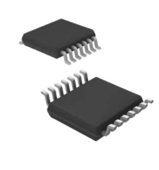


 工商网监
湘ICP备2023018690号
工商网监
湘ICP备2023018690号

