DAC7641
®
DAC
®
764
1
For most current data sheet and other product
information, visit www.burr-brown.com
16-Bit, Voltage Output
DIGITAL-TO-ANALOG CONVERTER
FEATURES
DESCRIPTION
● LOW POWER: 2.5mW
● UNIPOLAR OR BIPOLAR OPERATION
● SETTLING TIME: 10µs to 0.003%
● 15-BIT LINEARITY AND MONOTONICITY:
–40°C to +85°C
The DAC7641 is a 16-bit, voltage output digital-toanalog converter (DAC) with guaranteed 15-bit monotonic performance over the specified temperature range.
It accepts 16-bit parallel input data, has double-buffered
DAC input logic (allowing asynchronous update), and
provides a readback mode of the internal input registers.
Programmable asynchronous reset clears all registers to
a mid-scale code of 8000H or to a zero-scale of 0000H.
The DAC7641 can operate from a single +5V supply or
from +5V and –5V supplies.
Low power and small size per DAC make the DAC7641
ideal for automatic test equipment, DAC-per-pin
programmers, data acquisition systems, and closedloop servo-control. The DAC7641 is available in a
TQFP-32 package, and offers guaranteed specifications over the –40°C to +85°C temperature range.
● PROGRAMMABLE RESET TO MID-SCALE
OR ZERO-SCALE
● DATA READBACK
● DOUBLE-BUFFERED DATA INPUTS
APPLICATIONS
● PROCESS CONTROL
● ATE PIN ELECTRONICS
● CLOSED-LOOP SERVO-CONTROL
● MOTOR CONTROL
● DATA ACQUISITION SYSTEMS
● DAC-PER-PIN PROGRAMMERS
VDD
16
DATA I/O
I/O
Buffer
CS
R/W
Control
Logic
VSS
VREFL
Sense
VCC
DAC
Register
Input
Register
VREFL
VREFH
VREFH
Sense
DAC
VOUT
VOUT Sense
DAC7641
AGND
DGND
RST
RSTSEL
LDAC
International Airport Industrial Park • Mailing Address: PO Box 11400, Tucson, AZ 85734 • Street Address: 6730 S. Tucson Blvd., Tucson, AZ 85706 • Tel: (520) 746-1111
Twx: 910-952-1111 • Internet: http://www.burr-brown.com/ • Cable: BBRCORP • Telex: 066-6491 • FAX: (520) 889-1510 • Immediate Product Info: (800) 548-6132
®
© 2000 Burr-Brown Corporation
SBAS118
PDS-1532A
1
Printed in U.S.A. June, 2000
DAC7641
�SPECIFICATIONS (Dual Supply)
At TA = TMIN to TMAX, VDD = VCC = +5V, VSS = –5V, VREFH = +2.5V, and VREFL = –2.5V, unless otherwise noted.
DAC7641Y
PARAMETER
CONDITIONS
ACCURACY
Linearity Error
Differential Linearity Error
Monotonicity, TMIN to TMAX
Bipolar Zero Error
Bipolar Zero Error Drift
Full-Scale Error
Full-Scale Error Drift
Power Supply Rejection Ratio (PSRR)
ANALOG OUTPUT
Voltage Output
Output Current
Maximum Load Capacitance
Short-Circuit Current
Short-Circuit Duration
TYP
MAX
±3
±2
±4
±3
±1
5
±1
5
10
±3
10
±3
10
100
14
At Full Scale
VREF = –2.5V, RL = 10kΩ, VSS = –5V
MIN
VREFH
+1.25
VREFL + 1.25
–2.5
+2.5
VREFH – 1.25
8
2
60
40
f = 10kHz
7FFFH to 8000H or 8000H to 7FFFH
DIGITAL INPUT
VIH
VIL
IIH
IIL
UNITS
±2
±1
±3
±2
✻
✻
✻
✻
✻
✻
✻
✻
✻
✻
LSB
LSB
Bits
mV
ppm/°C
mV
ppm/°C
ppm/V
✻
✻
✻
✻
✻
✻
10
POWER SUPPLY
VDD
VCC
VSS
ICC
IDD
ISS
Power
3.6
+4.75
+4.75
–5.25
–0.6
TEMPERATURE RANGE
Specified Performance
–40
✻
✻
V
V
µA
µA
✻
µs
nV-s
nV/√Hz
nV-s
✻
0.3 • VDD
±10
±10
IOH = –0.8mA
IOL = 1.2mA
V
mA
pF
mA
✻
✻
0.7 • VDD
DIGITAL OUTPUT
VOH
VOL
✻
✻
✻
✻
✻
500
–500
To ±0.003%, 5V Output Step
MAX
✻
✻
500
–10, +30
Indefinite
GND or VCC or VSS
TYP
15
VREFL
–1.25
No Oscillation
REFERENCE INPUT
Ref High Input Voltage Range
Ref Low Input Voltage Range
Ref High Input Current
Ref Low Input Current
DYNAMIC PERFORMANCE
Settling Time
Digital Feedthrough
Output Noise Voltage
DAC Glitch
MIN
DAC7641YB
4.5
0.3
+5.0
+5.0
–5.0
0.4
15
–0.5
4
✻
0.4
+5.25
+5.25
–4.75
0.5
✻
✻
✻
–0.4
5.5
✻
+85
✻
✻
✻
✻
✻
✻
✻
✻
✻
✻
✻
✻
✻
V
V
µA
µA
✻
V
V
✻
✻
✻
✻
✻
V
V
V
mA
µA
mA
mW
✻
°C
✻ Specifications same as DAC7641Y.
The information provided herein is believed to be reliable; however, BURR-BROWN assumes no responsibility for inaccuracies or omissions. BURR-BROWN assumes
no responsibility for the use of this information, and all use of such information shall be entirely at the user’s own risk. Prices and specifications are subject to change
without notice. No patent rights or licenses to any of the circuits described herein are implied or granted to any third party. BURR-BROWN does not authorize or warrant
any BURR-BROWN product for use in life support devices and/or systems.
®
DAC7641
2
�SPECIFICATIONS (Single Supply)
At TA = TMIN to TMAX, VDD = VCC = +5V, VSS = 0V, VREFH = +2.5V, and VREFL = 0V, unless otherwise noted.
DAC7641Y
PARAMETER
ACCURACY
Linearity Error(1)
Differential Linearity Error
Monotonicity, TMIN to TMAX
Zero Scale Error
Zero Scale Error Drift
Full-Scale Error
Full-Scale Error Drift
Power Supply Rejection Ratio (PSRR)
ANALOG OUTPUT
Voltage Output
Output Current
Maximum Load Capacitance
Short-Circuit Current
Short-Circuit Duration
CONDITIONS
At Full Scale
VREFL = 0V, VSS = 0V, RL = 10kΩ
POWER SUPPLY
VDD
VCC
VSS
ICC
IDD
Power
TEMPERATURE RANGE
Specified Performance
MAX
±3
±2
±4
±3
±1
5
±1
5
10
±3
10
±3
10
100
MIN
VREFH
+1.25
VREFL + 1.25
0
+2.5
VREFH – 1.25
8
2
60
40
7FFFH to 8000H or 8000H to 7FFFH
UNITS
±2
±1
±3
±2
✻
✻
✻
✻
✻
✻
✻
✻
✻
✻
LSB
LSB
Bits
mV
ppm/°C
mV
ppm/°C
ppm/V
✻
✻
✻
✻
✻
✻
10
+4.75
+4.75
0
–40
✻
✻
V
V
µA
µA
✻
µs
nV-s
nV/√Hz
nV-s
✻
0.3 • VDD
±10
±10
3.6
V
mA
pF
mA
✻
✻
0.7 • VDD
IOH = –0.8mA
IOL = 1.2mA
✻
✻
✻
✻
✻
250
–250
To ±0.003%, 2.5V Output Step
MAX
✻
✻
500
±30
Indefinite
GND or VCC
TYP
15
0
–1.25
No Oscillation
DIGITAL INPUT
VIH
VIL
IIH
IIL
DIGITAL OUTPUT
VOH
VOL
TYP
14
REFERENCE INPUT
Ref High Input Voltage Range
Ref Low Input Voltage Range
Ref High Input Current
Ref Low Input Current
DYNAMIC PERFORMANCE
Settling Time
Digital Feedthrough
Output Noise Voltage, f = 10kHz
DAC Glitch
MIN
DAC7641YB
4.5
0.3
+5.0
+5.0
0
0.4
15
1.8
✻
0.4
+5.25
+5.25
0
0.5
✻
✻
✻
2.5
+85
✻
✻
✻
✻
✻
✻
✻
✻
✻
✻
✻
✻
V
V
µA
µA
✻
V
V
✻
✻
✻
✻
✻
V
V
V
mA
µA
mW
✻
°C
✻ Specifications same as DAC7641Y.
NOTE: (1) If VSS = 0V specification applies at Code 0040H and above due to possible negative zero-scale error.
®
3
DAC7641
�ELECTROSTATIC
DISCHARGE SENSITIVITY
ABSOLUTE MAXIMUM RATINGS(1)
VSS to VSS ............................................................................. –0.3V to 11V
VDD to GND .......................................................................... –0.3V to 5.5V
VREFL to GND ............................................................ –0.3V to (VSS – VCC)
VREFH to GND ........................................................... –0.3V to (VSS – VCC)
VREFH to VREFL .................................................................... –0.3V to +11V
Digital Input Voltage to GND ................................... –0.3V to VDD + 0.3V
Digital Output Voltage to GND ................................. –0.3V to VDD + 0.3V
Maximum Junction Temperature ................................................... +150°C
Operating Temperature Range ........................................ –40°C to +85°C
Storage Temperature Range ......................................... –65°C to +150°C
Lead Temperature (soldering, 10s) ............................................... +300°C
This integrated circuit can be damaged by ESD. Burr-Brown
recommends that all integrated circuits be handled with
appropriate precautions. Failure to observe proper handling
and installation procedures can cause damage.
ESD damage can range from subtle performance degradation
to complete device failure. Precision integrated circuits may
be more susceptible to damage because very small parametric
changes could cause the device not to meet its published
specifications.
NOTE: (1) Stresses above those listed under “Absolute Maximum Ratings”
may cause permanent damage to the device. Exposure to absolute maximum
conditions for extended periods may affect device reliability.
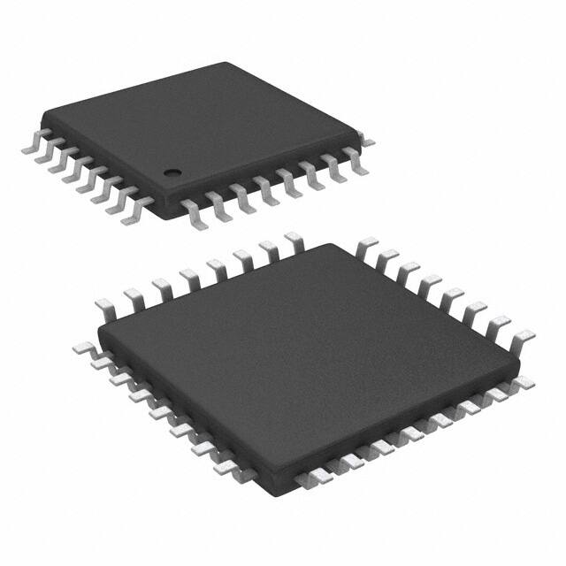
PACKAGE/ORDERING INFORMATION
PRODUCT
DAC7641Y
"
DAC7641YB
"
MINIMUM
RELATIVE
ACCURACY
(LSB)
DIFFERENTIAL
NONLINEARITY
(LSB)
±4
"
±3
"
±3
"
±2
"
PACKAGE
PACKAGE
DRAWING
NUMBER
SPECIFICATION
TEMPERATURE
RANGE
ORDERING
NUMBER(1)
TQFP-32
"
TQFP-32
"
351
"
351
"
–40°C to +85°C
"
–40°C to +85°C
"
DAC7641Y/250
DAC7641Y/2K
DAC7641YB/250
DAC7641YB/2K
TRANSPORT
MEDIA
Tape
Tape
Tape
Tape
and
and
and
and
Reel
Reel
Reel
Reel
NOTES: (1) Models with a slash (/) are available only in Tape and Reel in the quantities indicated (e.g., /2K indicates 2000 devices per reel). Ordering 2000 pieces
of “DAC7641Y/2K” will get a single 2000-piece Tape and Reel.
®
DAC7641
4
�25 AGND
26 VCC
27 VREFH Sense
28 VREFH
29 VREFL Sense
30 VREFL
31 DGND
32 VDD
PIN CONFIGURATION
DB15
1
24
VSS
DB14
2
23
VOUT Sense
DB13
3
22
VOUT
DB12
4
21
RSTSEL
DAC7641
16
CS
DB0
17
15
8
DB1
DB8
14
R/W
DB2
18
13
7
DB3
DB9
12
LDAC
DB4
19
11
6
DB5
DB10
10
RST
DB6
20
9
5
DB7
DB11
PIN DESCRIPTIONS
PIN
NAME
DESCRIPTION
PIN
NAME
DESCRIPTION
1
DB15
Data Bit 15, MSB
19
LDAC
2
DB14
Data Bit 14
20
RST
3
DB13
Data Bit 13
4
DB12
Data Bit 12
Reset, rising-edge triggered. Depending on the state
of RSTSEL, the DAC registers are set to either midscale or zero.
5
DB11
Data Bit 11
21
RSTSEL
6
DB10
Data Bit 10
7
DB9
Data Bit 9
Reset Select. Determines the action of RST. If
HIGH, a RST command will set the DAC registers to
mid-scale. If LOW, a RST command will set the DAC
registers to zero.
8
DB8
Data Bit 8
22
VOUT
9
DB7
Data Bit 7
23
VOUT Sense
10
DB6
Data Bit 6
11
DB5
Data Bit 5
24
VSS
12
DB4
Data Bit 4
25
AGND
13
DB3
Data Bit 3
26
VCC
14
DB2
Data Bit 2
27
VREFH Sense
15
DB1
Data Bit 1
28
VREFH
16
DB0
Data Bit 0, LSB
29
VREFL Sense
17
CS
Chip Select, active low.
30
VREFL
DAC Reference Low Input
18
R/W
Enabled by CS, controls data read and write from the
input register.
31
DGND
Digital Ground
32
VDD
DAC Load Strobe, rising-edge triggered.
DAC Voltage Output
DAC Output Amplifier Inverting Input. Used to close
the feedback loop at the load.
Negative Power Supply
Analog Ground
Positive Power Supply
DAC Reference High Sense Input
DAC Reference High Input
DAC Reference Low Sense Input
Positive Power Supply
®
5
DAC7641
�TYPICAL PERFORMANCE CURVES: VSS = 0V
At TA = +25°C, VDD = +5V, VSS = 0V, VREFH = +2.5V, VREFL = 0V, representative unit, unless otherwise specified.
LINEARITY ERROR AND
DIFFERENTIAL LINEARITY ERROR vs CODE
(+85°C)
LE (LSB)
3.0
2.0
1.0
0
–1.0
–2.0
–3.0
2.0
1.5
1.0
0.5
0
–0.5
–1.0
–1.5
–2.0
0000H 2000H 4000H 6000H 8000H A000H C000H E000H FFFFH
DLE (LSB)
DLE (LSB)
LE (LSB)
LINEARITY ERROR AND
DIFFERENTIAL LINEARITY ERROR vs CODE
(+25°C)
3.0
2.0
1.0
0
–1.0
–2.0
–3.0
2.0
1.5
1.0
0.5
0
–0.5
–1.0
–1.5
–2.0
0000H 2000H 4000H 6000H 8000H A000H C000H E000H FFFFH
Digital Input Code
Digital Input Code
DLE (LSB)
ZERO-SCALE ERROR vs TEMPERATURE
2
3.0
2.0
1.0
0
–1.0
–2.0
–3.0
Code (0040H)
1.5
1
UPO (mV)
LE (LSB)
LINEARITY ERROR AND
DIFFERENTIAL LINEARITY ERROR vs CODE
(–40°C)
2.0
1.5
1.0
0.5
0
–0.5
–1.0
–1.5
–2.0
0000H 2000H 4000H 6000H 8000H A000H C000H E000H FFFFH
0.5
0
–0.5
–1
–1.5
–2
–40 –30 –20 –10 0
10 20 30 40 50 60 70 80
90
Temperature (°C)
Digital Input Code
POSITIVE FULL-SCALE ERROR vs TEMPERATURE
VREFH CURRENT vs CODE
0.14
2
0.12
1
VREF Current (mA)
Positive Full-Scale Error (mV)
Code (FFFFH)
1.5
0.5
0
–0.5
–1
0.10
0.08
0.06
0.04
0.02
–1.5
0.00
0000H 2000H 4000H 6000H 8000H A000H C000H E000H FFFFH
–2
–40 –30 –20 –10 0
10 20 30 40 50 60 70 80
90
Temperature (°C)
Digital Input Code
®
DAC7641
6
�TYPICAL PERFORMANCE CURVES: VSS = 0V
(Cont.)
At TA = +25°C, VDD = +5V, VSS = 0V, VREFH = +2.5V, VREFL = 0V, representative unit, unless otherwise specified.
VREFL CURRENT vs CODE
POWER SUPPLY CURRENT vs TEMPERATURE
1.0
0.00
Quiescent Current (mA)
VREF Current (mA)
Data = FFFFH
No Load
0.8
–0.02
–0.04
–0.06
–0.08
–0.10
–0.12
0.6
ICC
0.4
0.2
0.0
–0.2
–0.4
–0.6
–0.8
–1.0
–0.14
0000H 2000H 4000H 6000H 8000H A000H C000H E000H FFFFH
–40 –30 –20 –10 0
10 20 30 40 50 60 70 80 90
Digital Input Code
Temperature (°C)
POSITIVE SUPPLY CURRENT
vs DIGITAL INPUT CODE
OUTPUT VOLTAGE vs SETTLING TIME
(0V to +2.5V)
+5V
LDAC
0
0.50
0.45
Large-Signal Settling Time: 0.5V/div
0.40
Output Voltage
0.30
ICC
0.25
0.20
0.15
Small-Signal Settling Time: 4LSB/div
0.10
0.05
0.00
0000H 0200H 0400H 0800H 1000H 2000H 4000H 6000H 8000H A000H C000H E000H FFFFH
Time (2µs/div)
Digital Input Code
OUTPUT VOLTAGE
vs MIDSCALE GLITCH PERFORMANCE
OUTPUT VOLTAGE vs SETTLING TIME
(+2.5V to 2mV)
+5V
LDAC
0
Output Voltage (50mV/div)
+5V
LDAC
0
Output Voltage
ICC (mA)
0.35
Small-Signal Settling Time: 4LSB/div
Large-Signal Settling Time: 0.5V/div
7FFFH to 8000H
Time (1µs/div)
Time (2µs/div)
®
7
DAC7641
�TYPICAL PERFORMANCE CURVES: VSS = 0V
(Cont.)
At TA = +25°C, VDD = +5V, VSS = 0V, VREFH = +2.5V, VREFL = 0V, representative unit, unless otherwise specified.
OUTPUT VOLTAGE
vs MIDSCALE GLITCH PERFORMANCE
BROADBAND NOISE
Noise Voltage (50µV/div)
Output Voltage (50mV/div)
+5V
LDAC
0
8000H to 7FFFH
BW = 10kHz
Code = 8000H
Time (1µs/div)
Time (10ms/div)
OUTPUT NOISE VOLTAGE vs FREQUENCY
LOGIC SUPPLY CURRENT
vs LOGIC INPUT LEVEL FOR DATA BITS
12
Logic Supply Current (mA)
100
10
8
6
4
2
0
10
100
10
1000
100000
10000
1
0
1000000
2
OUTPUT VOLTAGE vs RLOAD
5
4
3
Source
2
1
0
0.01
Sink
0.1
1
RLOAD (kΩ)
®
DAC7641
3
Logic Input Level for Data Bits (V)
Frequency (Hz)
VOUT (V)
Noise (nV/√Hz)
1000
8
10
100
4
5
�TYPICAL PERFORMANCE CURVES: VSS = –5V
At TA = +25°C, VDD = +5V, VSS = –5V, VREFH = +2.5V, VREFL = –2.5V, representative unit, unless otherwise specified.
LINEARITY ERROR AND
DIFFERENTIAL LINEARITY ERROR vs CODE
(+85°C)
LE (LSB)
3.0
2.0
1.0
0
–1.0
–2.0
–3.0
2.0
1.5
1.0
0.5
0
–0.5
–1.0
–1.5
–2.0
0000H 2000H 4000H 6000H 8000H A000H C000H E000H FFFFH
DLE (LSB)
DLE (LSB)
LE (LSB)
LINEARITY ERROR AND
DIFFERENTIAL LINEARITY ERROR vs CODE
(+25°C)
3.0
2.0
1.0
0
–1.0
–2.0
–3.0
2.0
1.5
1.0
0.5
0
–0.5
–1.0
–1.5
–2.0
0000H 2000H 4000H 6000H 8000H A000H C000H E000H FFFFH
Digital Input Code
Digital Input Code
VREFH CURRENT vs CODE
3.0
2.0
1.0
0
–1.0
–2.0
–3.0
0.30
0.25
VREF Current (mA)
DLE (LSB)
LE (LSB)
LINEARITY ERROR AND
DIFFERENTIAL LINEARITY ERROR vs CODE
(–40°C)
2.0
1.5
1.0
0.5
0
–0.5
–1.0
–1.5
–2.0
0000H 2000H 4000H 6000H 8000H A000H C000H E000H FFFFH
0.15
0.10
0.05
0.00
0000H 2000H 4000H 6000H 8000H A000H C000H E000H FFFFH
Digital Input Code
Digital Input Code
VREFL CURRENT vs CODE
ZERO-SCALE ERROR vs TEMPERATURE
(Code 8000H)
0.00
2
1.5
Zero-Scale Error (mV)
–0.05
VREF Current (mA)
0.20
–0.10
–0.15
–0.20
–0.25
1
0.5
0
–0.5
–1
–1.5
–2
–0.30
0000H 2000H 4000H 6000H 8000H A000H C000H E000H FFFFH
–40 –30 –20 –10 0
10 20 30 40 50 60 70 80
90
Temperature (°C)
Digital Input Code
®
9
DAC7641
�TYPICAL PERFORMANCE CURVES: VSS = –5V
(Cont.)
At TA = +25°C, VDD = +5V, VSS = –5V, VREFH = +2.5V, VREFL = –2.5V, representative unit, unless otherwise specified.
NEGATIVE FULL-SCALE ERROR vs TEMPERATURE
(Code 0000H)
2
2
1.5
1.5
Negative Full-Scale Error (mV)
Positive Full-Scale Error (mV)
POSITIVE FULL-SCALE ERROR vs TEMPERATURE
(Code FFFFH)
1
0.5
0
–0.5
–1
–1.5
1
0.5
0
–0.5
–1
–1.5
–2
–2
–40 –30 –20 –10 0
10 20 30 40 50 60 70 80
–40 –30 –20 –10 0
90
POWER SUPPLY CURRENT
vs TEMPERATURE
5
Data = FFFFH
No Load
4
0.6
Source
3
ICC
0.4
2
0.2
VOUT (V)
Quiescent Current (mA)
90
OUTPUT VOLTAGE vs RLOAD
1.0
0.8
10 20 30 40 50 60 70 80
Temperature (°C)
Temperature (°C)
0.0
–0.2
ISS
–0.4
1
0
–1
Sink
–2
–0.6
–3
–0.8
–4
–1.0
–40 –30 –20 –10 0
–5
0.01
10 20 30 40 50 60 70 80 90
Temperature (°C)
0.1
1
10
100
RLOAD (kΩ)
POSITIVE SUPPLY CURRENT
vs DIGITAL INPUT CODE
OUTPUT VOLTAGE vs SETTLING TIME
(–2.5V to +2.5V)
0.50
0.45
0.40
Large-Signal Settling Time: 1V/div
ICC
Output Voltage
ICC (mA)
0.35
0.30
0.25
0.20
0.15
Small-Signal Settling Time: 2LSB/div
0.10
0.05
0.00
0000H 0200H 0400H 0800H 1000H 2000H 4000H 6000H 8000H A000H C000H E000H FFFFH
Time (2µs/div)
Digital Input Code
®
DAC7641
10
+5V
LDAC
0
�TYPICAL PERFORMANCE CURVES: VSS = –5V
(Cont.)
At TA = +25°C, VDD = +5V, VSS = –5V, VREFH = +2.5V, VREFL = –2.5V, representative unit, unless otherwise specified.
OUTPUT VOLTAGE vs SETTLING TIME
(+2.5V to –2.5V)
+5V
LDAC
0
Output Voltage
Small-Signal Settling Time:
2LSB/div
Large-Signal Settling Time: 1V/div
Time (2µs/div)
THEORY OF OPERATION
references VREFL and VREFH, respectively. The digital input
is a 16-bit parallel word and the DAC input register offers a
readback capability. The converters can be powered from
either a single +5V supply or a dual ±5V supply. The device
offers a reset function which immediately sets all DAC
output voltages and DAC registers to mid-scale code 8000H
or to zero-scale code 0000H. See Figures 2 and 3 for the
basic operation of the DAC7641.
The DAC7641 is a voltage output, 16-bit digital-to-analog
converter (DAC). The architecture is an R-2R ladder configuration with the three MSBs segmented, followed by an
operational amplifier that serves as a buffer (see Figure 1).
The minimum voltage output (zero-scale) and maximum
voltage output (full-scale) are set by the external voltage
RF
VOUT Sense
VOUT
R
2R
2R
2R
2R
2R
2R
2R
2R
2R
VREFH
VREFH Sense
VREFL
VREFL Sense
FIGURE 1. DAC7641 Architecture.
®
11
DAC7641
�+5V
1µF
+
0.1µF
0V
DGND
32
31
VDD
30
1
2
3
4
5
6
7
8
29
28
27
VREFH
VREFL
DGND
26
25
VCC
VREFH
Sense
VREFL
Sense
AGND
DB15
VSS
DB14
VOUT Sense
DB13
VOUT
DAC7641
DB12
AGND
+2.5000V
RSTSEL
DB11
RST
DB10
LDAC
DB9
R/W
DB8
CS
24
23
22
0V to +2.5V
21
DAC RESET MODE SELECT
20
DAC RESET
19
DAC LOAD STROBE
18
READ/WRITE STROBE
17
CHIP SELECT
DB7 DB6 DB5 DB4 DB3 DB2 DB1 DB0
9 10 11 12 13 14 15 16
FIGURE 2. Single-Supply Operation.
+5V
1µF
+
1µF
+
0.1µF
0.1µF
–2.500V +2.500V
–5V
DGND
32
31
VDD
DGND
1
2
3
4
5
6
7
8
30
29
28
27
VREFL
Sense
26
25
AGND
VCC
VREFH
VREFL
VREFH
Sense
AGND
DB15
VSS
DB14
VOUT Sense
DB13
VOUT
DB12
DAC7641
RSTSEL
DB11
RST
DB10
LDAC
DB9
R/W
DB8
CS
DB7 DB6 DB5 DB4 DB3 DB2 DB1 DB0
9 10 11 12 13 14 15 16
FIGURE 3. Dual-Supply Operation.
®
DAC7641
12
24
23
22
21
20
19
18
17
–2.5V to +2.5V
DAC RESET MODE SELECT
DAC RESET
DAC LOAD STROBE
READ/WRITE STROBE
CHIP SELECT
�ANALOG OUTPUTS
When VSS = –5V (dual supply operation), the output amplifier can swing to within 2.25V of the supply rails, guaranteed over the –40°C to +85°C temperature range. With VSS
= 0V (single-supply operation), and with RLOAD also connected to ground, the output can swing to ground. Care must
be taken when measuring the zero-scale error with VSS = 0V.
Since the output voltage cannot swing below ground, the
output voltage may not change for the first few digital input
codes (0000H, 0001H, 0002H, etc.) if the output amplifier has
a negative offset. At the negative limit of –2mV, the first
specified output starts at code 0040H.
+V
Due to the high accuracy of these D/A converters, system
design problems such as grounding and contact resistance
become very important. A 16-bit converter with a 2.5V fullscale range has a 1LSB value of 38µV. With a load current
of 1mA, series wiring and connector resistance (see Figure
4) of only 40mΩ (RW2) will cause a voltage drop of 40µV.
To understand what this means in terms of a system layout,
the resistivity of a typical 1 ounce copper-clad printed circuit
board is 1/2 mΩ per square. For a 1mA load, a 10 milli-inch
wide printed circuit conductor 600 milli-inches long will
result in a voltage drop of 30µV.
VCC
AGND
26
25
VREFH Sense 27
VREFH 28
VREFL Sense 29
VREFL 30
+2.5V
24 VSS
RW1
VOUT Sense 23
VOUT
VOUT 22
RW2
DAC7641
FIGURE 4. Analog Output Closed-Loop Configuration. RW
represents wiring resistances.
connected to ground or must be in the range of –4.75V to
–5.25V. The voltage on VSS sets several bias points within
the converter. If VSS is not in one of these two configurations, the bias values may be in error and proper operation
of the device is not guaranteed.
The DAC7641 offers a force and sense output configuration
for the high open-loop gain output amplifier. This feature
allows the loop around the output amplifier to be closed at the
load (see Figure 4), thus ensuring an accurate output voltage.
The current into the VREFH input and out of VREFL depends
on the DAC output voltages and can vary from a few
microamps to approximately 0.5mA. The reference input
appears as a varying load to the reference. If the reference
can sink or source the required current, a reference buffer is
not required. The DAC7641 features a reference drive and
sense connection such that the internal errors caused by the
changing reference current and the circuit impedances can
be minimized. Figures 5 through 13 show different reference
configurations and the effect on the linearity and differential
linearity.
REFERENCE INPUTS
The reference inputs, VREFL and VREFH, can be any voltage
between VSS + 2.5V and VCC – 2.5V provided that VREFH is
at least 1.25V greater than VREFL. The minimum output of
each DAC is equal to VREFL plus a small offset voltage
(essentially, the offset of the output op amp). The maximum
output is equal to VREFH plus a similar offset voltage. Note
that VSS (the negative power supply) must either be
OPA2234
–2.5V
500pF
–V
VCC
AGND
26
25
VREFH Sense 27
VREFH 28
VREFL Sense 29
VREFL 30
500pF
+V
+2.5V
24 VSS
VOUT Sense 23
VOUT
VOUT 22
DAC7641
FIGURE 5. Dual Supply Configuration-Buffered References, used for Dual Supply Performance Curves.
®
13
DAC7641
�OPA2350
2200pF
100Ω
0.05V
1000pF
2kΩ
100Ω
+V
98kΩ
2200pF
+2.5V
VCC
AGND
26
25
VREFH Sense 27
VREFH 28
VREFL Sense 29
VREFL 30
1000pF
24 VSS
VOUT Sense 23
VOUT
VOUT 22
DAC7641
NOTE: VREFL has been chosen to be 50mV to allow for current sinking voltage
drops across the 100Ω resistor and the output stage of the buffer op amp.
FIGURE 6. Single-Supply Buffered Reference with a Reference Low of 50mV.
LINEARITY ERROR AND
DIFFERENTIAL LINEARITY ERROR vs CODE
(+25°C)
LE (LSB)
2.0
1.5
1.0
0.5
0
–0.5
–1.0
–1.5
–2.0
2.0
1.5
1.0
0.5
0
–0.5
–1.0
–1.5
–2.0
0000H 2000H 4000H 6000H 8000H A000H C000H E000H FFFFH
DLE (LSB)
DLE (LSB)
LE (LSB)
LINEARITY ERROR AND
DIFFERENTIAL LINEARITY ERROR vs CODE
(+25°C)
2.5
2.0
1.5
1.0
0.5
0
–0.5
–1.0
–1.5
0000H 2000H 4000H 6000H 8000H A000H C000H E000H FFFFH
Digital Input Code
Digital Input Code
FIGURE 8. Integral Linearity and Differential Linearity
Error Curves for Figure 9.
FIGURE 7. Integral Linearity and Differential Linearity
Error Curves for Figure 6.
®
DAC7641
2.5
2.0
1.5
1.0
0.5
0
–0.5
–1.0
–1.5
14
�OPA2350
+V
2200pF
100Ω
+1.25V
100Ω
1000pF
+V
2200pF
VCC
AGND
26
25
+2.5V
VREFH Sense 27
VREFH 28
VREFL Sense 29
VREFL 30
1000pF
24 VSS
VOUT Sense 23
VOUT
VOUT 22
DAC7641
FIGURE 9. Single-Supply Buffered Reference with VREFL = +1.25V and VREFH = +2.5V.
+V
LINEARITY ERROR AND
DIFFERENTIAL LINEARITY ERROR vs CODE
(+25°C)
+2.5V
100Ω
OPA350
AGND
25
LE (LSB)
VCC
26
24 VSS
DLE (LSB)
VREFH Sense 27
2200pF
VREFH 28
VREFL Sense 29
VREFL 30
1000pF
VOUT Sense 23
VOUT 22
VOUT
DAC7641
3.0
2.5
2.0
1.5
1.0
0.5
0
–0.5
–1.0
2.0
1.5
1.0
0.5
0
–0.5
–1.0
–1.5
–2.0
0000H 2000H 4000H 6000H 8000H A000H C000H E000H FFFFH
Digital Input Code
FIGURE 10. Single-Supply Buffered VREFH.
FIGURE 11. Linearity and Differential Linearity Error Curves
for Figure 10.
®
15
DAC7641
�LINEARITY ERROR AND
DIFFERENTIAL LINEARITY ERROR vs CODE
(+25°C)
+V
AGND
25
LE (LSB)
VCC
26
24 VSS
DLE (LSB)
VREFH Sense 27
VREFH 28
VREFL Sense 29
VREFL 30
+2.5V
VOUT Sense 23
VOUT
VOUT 22
DAC7641
2.5
2.0
1.5
1.0
0.5
0
–0.5
–1.0
–1.5
2.0
1.5
1.0
0.5
0
–0.5
–1.0
–1.5
–2.0
0000H 2000H 4000H 6000H 8000H A000H C000H E000H FFFFH
Digital Input Code
FIGURE 12. Low Cost Single-Supply Configuration.
FIGURE 13. Linearity and Differential Linearity Error Curves
for Figure 12.
DIGITAL INTERFACE
Table I shows the basic control logic for the DAC7641. Note
that the internal register is edge triggered and not level
triggered. When the LDAC signal is transitioned to HIGH,
the digital word currently in the register is latched.
DIGITAL TIMING
Figure 14 and Table II provide detailed timing for the digital
interface of the DAC7641.
DIGITAL INPUT CODING
The DAC7641 input data is in Straight Binary format. The
output voltage is given by Equation 1.
The double-buffered architecture is designed so that the
DAC input register can be written to at any time.
R/W
CS
L
H
X
X
X
X
L
L
H
H
X
X
RST RSTSEL LDAC REGISTER
H
H
H
H
↑
↑
X
X
X
X
L
H
X
X
↑
H
X
X
Write
Read
Hold
Hold
REGISTER
VOUT = VREF L +
INPUT
MODE
Hold
Write Input
Hold
Read Input
Write
Update
Hold
Hold
Reset to Zero
Reset to Zero
Reset to Midscale Reset to Midscale
65, 536
(1)
where N is the digital input code. This equation does not
include the effects of offset (zero-scale) or gain (full-scale)
errors.
TABLE I. DAC7641 Logic Truth Table.
®
DAC7641
(VREF H – VREF L) • N
16
�tWCS
CS
tRCS
tWS
CS
R/W
tRDH
tRDS
R/W
tLS
tLX
tLH
tLWD
tDZ
Data Out
tWH
±0.003% of FSR
Error Band
LDAC
Data Valid
tDH
tDS
tCSD
Data In
tS
Data Read Timing
VOUT
Data Write Timing
tSS
±0.003% of FSR
Error Band
tSH
RSTSEL
tRSH
tRSS
RST
+FS
VOUT, RSTSEL LOW
–FS
+FS
MS
VOUT, RSTSEL HIGH
–FS
DAC7641 Reset Timing
FIGURE 14. Digital Input and Output Timing.
SYMBOL
DESCRIPTION
MIN
tRCS
tRDS
tRDH
tDZ
tCSD
tWCS
tWS
tWH
tLS
tLH
tLX
tDS
tDH
tLWD
tSS
tSH
tRSS
tRSH
tS
CS LOW for Read
R/W HIGH to CS LOW
R/W HIGH after CS HIGH
CS HIGH to Data Bus in High Impedance
CS LOW to Data Bus Valid
CS LOW for Write
R/W LOW to CS LOW
R/W LOW after CS HIGH
CS LOW to LDAC HIGH
CS LOW after LDAC HIGH
LDAC HIGH
Data Valid to CS LOW
Data Valid after CS HIGH
LDAC LOW
RSTSEL Valid Before RESET HIGH
RSTSEL Valid After RESET HIGH
RESET LOW Before RESET HIGH
RESET LOW After RESET HIGH
Settling Time
150
10
10
10
TYP
100
MAX
100
150
40
0
10
30
100
100
0
10
100
0
200
10
10
10
UNITS
ns
ns
ns
ns
ns
ns
ns
ns
ns
ns
ns
ns
ns
ns
ns
ns
ns
ns
µs
TABLE II. Timing Specifications (TA = –40°C to +85°C).
®
17
DAC7641
�DIGITALLY-PROGRAMMABLE
CURRENT SOURCE
The DAC7641 offers a unique set of features that allows a
wide range of flexibility in designing applications circuits
such as programmable current sources. The DAC7641 offers
both a differential reference input as well as an open-loop
configuration around the output amplifier. The open-loop
configuration around the output amplifier allows transistor
to be placed within the loop to implement a digitallyprogrammable, uni-directional current source. The availability of a differential reference also allows programmability
for both the full-scale and zero-scale currents. The output
current is calculated as:
V H – VREF L N Value
I OUT = REF
•
R SENSE
65, 536
Figure 15 shows a DAC7641 in a 4mA to 20mA current
output configuration. The output current can be determined
by Equation 3:
(3)
2.5V – 0.5V N Value 0.5V
•
I OUT =
+
125Ω 65, 536 125Ω
At full-scale, the output current is 16mA plus the 4mA for
the zero current. At zero scale the output current is the offset
current of 4mA (0.5V/125Ω).
(2)
+ (VREF L / R SENSE )
OPA2350
2200pF
100Ω
+0.50v
20kΩ
1000pF
80kΩ
+V
100Ω
2200pF
VCC
AGND
25
VREFH Sense 27
VREFH 28
VREFL Sense 29
VREFL 30
1000pF
26
+2.5V
24 VSS
IOUT
VOUT Sense 23
VOUT 22
DAC7641
VPROGRAMMED
RSENSE
125Ω
FIGURE 15. 4-to-20mA Digitally Controlled Current Source.
®
DAC7641
18
�PACKAGE OPTION ADDENDUM
www.ti.com
7-Oct-2021
PACKAGING INFORMATION
Orderable Device
Status
(1)
Package Type Package Pins Package
Drawing
Qty
Eco Plan
(2)
Lead finish/
Ball material
MSL Peak Temp
Op Temp (°C)
Device Marking
(3)
(4/5)
(6)
DAC7641Y/250
ACTIVE
TQFP
PBS
32
250
RoHS & Green
Call TI
Level-3-260C-168 HR
-40 to 85
7641Y
DAC7641YB/250
ACTIVE
TQFP
PBS
32
250
RoHS & Green
Call TI
Level-3-260C-168 HR
-40 to 85
7641Y
B
(1)
The marketing status values are defined as follows:
ACTIVE: Product device recommended for new designs.
LIFEBUY: TI has announced that the device will be discontinued, and a lifetime-buy period is in effect.
NRND: Not recommended for new designs. Device is in production to support existing customers, but TI does not recommend using this part in a new design.
PREVIEW: Device has been announced but is not in production. Samples may or may not be available.
OBSOLETE: TI has discontinued the production of the device.
(2)
RoHS: TI defines "RoHS" to mean semiconductor products that are compliant with the current EU RoHS requirements for all 10 RoHS substances, including the requirement that RoHS substance
do not exceed 0.1% by weight in homogeneous materials. Where designed to be soldered at high temperatures, "RoHS" products are suitable for use in specified lead-free processes. TI may
reference these types of products as "Pb-Free".
RoHS Exempt: TI defines "RoHS Exempt" to mean products that contain lead but are compliant with EU RoHS pursuant to a specific EU RoHS exemption.
Green: TI defines "Green" to mean the content of Chlorine (Cl) and Bromine (Br) based flame retardants meet JS709B low halogen requirements of


 工商网监
湘ICP备2023018690号
工商网监
湘ICP备2023018690号
